EP0853785B1 - Self-modifying code handling system - Google Patents
Self-modifying code handling system Download PDFInfo
- Publication number
- EP0853785B1 EP0853785B1 EP96933906A EP96933906A EP0853785B1 EP 0853785 B1 EP0853785 B1 EP 0853785B1 EP 96933906 A EP96933906 A EP 96933906A EP 96933906 A EP96933906 A EP 96933906A EP 0853785 B1 EP0853785 B1 EP 0853785B1
- Authority
- EP
- European Patent Office
- Prior art keywords
- instruction
- store
- self
- address
- modifying code
- Prior art date
- Legal status (The legal status is an assumption and is not a legal conclusion. Google has not performed a legal analysis and makes no representation as to the accuracy of the status listed.)
- Expired - Lifetime
Links
Images


Classifications
-
- G—PHYSICS
- G06—COMPUTING OR CALCULATING; COUNTING
- G06F—ELECTRIC DIGITAL DATA PROCESSING
- G06F9/00—Arrangements for program control, e.g. control units
- G06F9/06—Arrangements for program control, e.g. control units using stored programs, i.e. using an internal store of processing equipment to receive or retain programs
- G06F9/30—Arrangements for executing machine instructions, e.g. instruction decode
- G06F9/38—Concurrent instruction execution, e.g. pipeline or look ahead
- G06F9/3818—Decoding for concurrent execution
- G06F9/382—Pipelined decoding, e.g. using predecoding
-
- G—PHYSICS
- G06—COMPUTING OR CALCULATING; COUNTING
- G06F—ELECTRIC DIGITAL DATA PROCESSING
- G06F9/00—Arrangements for program control, e.g. control units
- G06F9/06—Arrangements for program control, e.g. control units using stored programs, i.e. using an internal store of processing equipment to receive or retain programs
- G06F9/30—Arrangements for executing machine instructions, e.g. instruction decode
- G06F9/30145—Instruction analysis, e.g. decoding, instruction word fields
- G06F9/30149—Instruction analysis, e.g. decoding, instruction word fields of variable length instructions
-
- G—PHYSICS
- G06—COMPUTING OR CALCULATING; COUNTING
- G06F—ELECTRIC DIGITAL DATA PROCESSING
- G06F9/00—Arrangements for program control, e.g. control units
- G06F9/06—Arrangements for program control, e.g. control units using stored programs, i.e. using an internal store of processing equipment to receive or retain programs
- G06F9/30—Arrangements for executing machine instructions, e.g. instruction decode
- G06F9/3017—Runtime instruction translation, e.g. macros
- G06F9/30174—Runtime instruction translation, e.g. macros for non-native instruction set, e.g. Javabyte, legacy code
-
- G—PHYSICS
- G06—COMPUTING OR CALCULATING; COUNTING
- G06F—ELECTRIC DIGITAL DATA PROCESSING
- G06F9/00—Arrangements for program control, e.g. control units
- G06F9/06—Arrangements for program control, e.g. control units using stored programs, i.e. using an internal store of processing equipment to receive or retain programs
- G06F9/30—Arrangements for executing machine instructions, e.g. instruction decode
- G06F9/38—Concurrent instruction execution, e.g. pipeline or look ahead
- G06F9/3802—Instruction prefetching
- G06F9/3812—Instruction prefetching with instruction modification, e.g. store into instruction stream
-
- G—PHYSICS
- G06—COMPUTING OR CALCULATING; COUNTING
- G06F—ELECTRIC DIGITAL DATA PROCESSING
- G06F9/00—Arrangements for program control, e.g. control units
- G06F9/06—Arrangements for program control, e.g. control units using stored programs, i.e. using an internal store of processing equipment to receive or retain programs
- G06F9/30—Arrangements for executing machine instructions, e.g. instruction decode
- G06F9/38—Concurrent instruction execution, e.g. pipeline or look ahead
- G06F9/3818—Decoding for concurrent execution
- G06F9/3822—Parallel decoding, e.g. parallel decode units
-
- G—PHYSICS
- G06—COMPUTING OR CALCULATING; COUNTING
- G06F—ELECTRIC DIGITAL DATA PROCESSING
- G06F9/00—Arrangements for program control, e.g. control units
- G06F9/06—Arrangements for program control, e.g. control units using stored programs, i.e. using an internal store of processing equipment to receive or retain programs
- G06F9/30—Arrangements for executing machine instructions, e.g. instruction decode
- G06F9/38—Concurrent instruction execution, e.g. pipeline or look ahead
- G06F9/3836—Instruction issuing, e.g. dynamic instruction scheduling or out of order instruction execution
- G06F9/3853—Instruction issuing, e.g. dynamic instruction scheduling or out of order instruction execution of compound instructions
Definitions
- the invention relates to processors, and in particular to a system for handling self-modifying code in a pipelined processor.
- EP-A-0 159 712 discloses a computer system including a CPU and a memory system, the CPU including a cache memory, in which the CPU is operated on a pipeline protocol.
- the computer system includes control means for controlling the data flow in such a system to avoid implementation of conflicting instructions in the pipeline.
- US-A-5 434 987 relates to a method and apparatus for preventing incorrect fetching of an instruction of a self-modifying code sequence with dependency on a buffered store.
- Computer programs are typically designed, coded and compiled with a simplifying assumption that the resulting object code will be executed in sequential order.
- modern processor design techniques seek to exploit opportunities for concurrent execution of machine instructions, i.e. instruction parallelism.
- pipelining techniques can be used to map instruction parallelism to multiple stages of a single functional unit or execution path.
- superscalar techniques which include out-of-order instruction issue, out-of-order instruction completion, and speculative execution of instructions, map instruction parallelism to multiple functional units or execution paths.
- Modern processor designs often exploit both pipelining and superscalar techniques.
- Out-of-order instruction issue involves the issuance of instructions to execution units with little regard for the actual order of instruction in executing code.
- a superscalar processor which exploits out-of-order issue need only be constrained by dependencies between the output (results) of a given instruction and the inputs (operands) of subsequent instructions in formulating its instruction dispatch sequence.
- Out-of-order completion is a technique which allows a given instruction to complete (e.g. store its result) prior to the completion of an instruction which precedes it in the program sequence.
- speculative execution involves the execution of an instruction sequence based on predicted outcomes (e.g. of a branch) and allows a processor to execute instructions without waiting for branch conditions to actually be evaluated.
- the instruction parallelism i.e. the number of instructions available for parallel execution
- speculative execution see Johnson. Superscalar Processor Design. Prentice-Hall. Inc., New Jersey, 1991, pp.63-77 for an analysis).
- Superscalar techniques largely concern processor organisation independent of instruction set and other architectural features. Thus, one of the attractions of superscalar techniques is the possibility of developing a processor that is code compatible with an existing processor architecture, for example the x86 processor architecture. Many superscalar techniques apply equally well to either RISC or CISC architectures. However, because of the regularity of many of the RISC architectures, superscalar techniques have initially been applied to RISC processor designs. In particular, the three operand load/store architecture, fixed instruction lengths, limited addressing modes, and fixed-width registers associated with a RISC architecture and instruction set facilitate the single cycle decoding of multiple instructions necessary to consistently supply multiple execution units with work.
- Executing instructions out of sequential order can increase a superscalar processor's performance by allowing the superscalar processor to keep multiple execution units operating in parallel and thereby improve throughput. Accordingly, a scheduler for a superscalar processor can improve overall performance by determining which instructions can be executed out-of-order and providing, or dispatching, those instructions to appropriate execution units.
- a scheduler for a superscalar processor must also handle interrupts and traps. Many processor architectures, including the x86 processor architecture, require that an architectural state be known just before or after an instruction generates an error, interrupt, or trap. This presents a difficulty when instructions are executed out of sequential order. Therefore, the scheduler must be able to undo instructions and reconstruct the system's state as if instructions executed in sequential order.
- Self-modifying code represents a further complication.
- one part of an executing program may modify other pans of the same program.
- the modified instruction sequence parts may then be executed.
- Pipelining particularly the deep pipelining that is common in high-performance implementations of CISC architectures, results in large instruction processing latencies and high degrees of overlap between the processing of successive instructions.
- the execution of a memory write generally takes place late in such pipelines. Consequently, actions such as fetching instructions from memory or cache and speculatively dispatching instructions to execution pipelines can easily occur before the completion of a memory write which precedes the fetched or dispatched instruction in the execution sequence.
- a processor which includes tags indicating memory addresses for instructions advancing through pipeline stages of the processor and which includes an instruction decoder having a store target address buffer allows self-modifying code support logic to detect store operations writing into the instruction stream and trigger a self-modifying code fault.
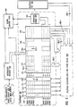
- FIGURE 1 is a block diagram of a superscalar computer processor providing out-of-order execution control in accordance with an embodiment of the present invention.
- FIGURE 2 is a block diagram of a scheduler constructed in accordance with an embodiment of the present invention.
- FIGURE 3 is a pipeline staging diagram illustrating architectural stages in the execution of instructions in accordance with an embodiment of the present invention.
- FIGURE 4 is a block diagram of out-of-order load and store execution control components in accordance with an embodiment of the present invention.
- FIGURE 5 is a block diagram of a computer system incorporating a processor that provides out-of-order load/store execution control in accordance with an embodiment of the present invention.
- FIGURE 1 depicts a superscalar processor embodiment of the present invention.
- Superscalar processor 100 includes an execution engine 150 which implements a reduced instruction set computing (RISC) architecture, an instruction decoder 140, caches, and a system interface 120 providing access to an address space represented in memory subsystem 122 and to devices on local busses (not shown).
- RISC reduced instruction set computing
- Superscalar processor 100 includes a cache which, in the embodiment described herein, is organized as separate data and instruction portions.
- Data cache 170 and instruction cache 130 are coupled (through cache control logic 160 and via system interface 120) to the address space represented in memory subsystem 122 which includes main memory and optionally includes additional levels of cache, illustratively an L2 cache.
- L2 cache control logic may be interposed between cache control logic 160 (for L1) and system interface 120.
- Cache system designs are well known in the art.
- suitable designs implementing split, "Harvard Architecture" instruction and data caches such as 170 and 130
- multi-level cache hierarchies are well known in the cache arts.
- the cache subsystem of superscalar processor 100 i.e., data cache 170, instruction cache 130, cache control logic 160, and an optional L2 cache
- instruction cache 130 is integrated with pre-decode logic (not shown).
- pre-decode logic identifies x86 instruction boundaries in the fetched instruction stream and facilitates the rapid decoding of instructions by instruction decoder 140.
- instruction sequences are loaded from the memory subsystem into instruction cache 130 for anticipated execution by execution engine 150.
- instructions in instruction cache 130 are CISC instructions selected from a complex instruction set such as the x86 instruction set implemented by processors conforming to the x86 processor architecture.
- Instruction decoder 140 converts CISC instructions received from instruction cache 130 to operations for execution engine 150. In the embodiment of FIGURE 1, these operations are RISC-like operations (hereafter OPs) and a single x86 instruction from instruction cache 130 decodes into one or more OPs for execution engine 150.
- OPs RISC-like operations
- OPs fall into one of several type groups including register operations (RegOps), load-store operations (LdStOps), load immediate value operations (LIMMOps), special operations (SpecOps), and floating point operations (FpOps).
- Register operations LdStOps
- LIMMOps load immediate value operations
- SpecOps special operations
- FpOps floating point operations
- Alternative embodiments may decode different instruction sets and supply different operation types for execution.
- Instruction decoder 140 includes two instruction translation portions, a hardware translation portion MacDec 141 and a ROM-based translation portion 142, together with branch prediction logic 143. Most common x86 instructions are translated into short sequences of 1 to 4 OPs using multiple parallel hardware decoders included in hardware translation portion 141. Hardware translation portion 141 decodes these common x86 instructions received from instruction cache 130 into short sequences of OPs which are then supplied to scheduler 180. Less common x86 instructions and those x86 instructions which translate into OP sequences longer than 4 OPs are translated by a ROM-based translation portion 142 which fetches (from ROM) a translated sequence of OPs corresponding to the particular x86 instruction to be translated. Translated OP sequences from either source, whether generated by hardware decoders or fetched from ROM, are supplied to scheduler 180 for execution by execution engine 150.
- execution engine 150 includes a scheduler 180, a register file 190, and multiple execution units which receive and execute OPs dispatched by scheduler 180.
- execution engine 150 includes seven execution units: load unit 152, store unit 153, register units 154 and 155, floating point unit 156, multimedia unit 157, and a branch unit 158, although alternative embodiments may add to or subtract from the set of execution units.
- floating point unit 156 and multimedia unit 157 are omitted.
- Execution engine 150 also includes a store queue 159 interposed between store unit 153 and data cache 170.
- Scheduler 180 is organized as an ordered array of storage entries and logic blocks coupled thereto, which together provide support for out-of-order dispatch of Ops to execution units and for forwarding of Op results to one or more execution units.
- the ordered array of storage entries and logic blocks also implements a reorder buffer and provides for renaming of the architectural registers defined in register file 190 and speculative execution recovery.
- Instruction decoder 140 supplies scheduler 180 with new Ops decoded from the instruction stream.
- scheduler 180 stores and maintains (in a storage entry) data associated with each new Op received. In this way scheduler 180 tracks the status of each Op and its associated data as the Op is issued to, and executed by, an execution unit. After a given Op is fully executed and data dependencies have been resolved, it is retired and the corresponding scheduler entry is released.
- Scheduler 180 is coupled to execution units (i.e., load unit 152, store unit 153, register units 154 and 155, floating point unit 156, multimedia unit 157, and branch unit 158) via a group of busses and control lines collectively shown as a bus 189.
- Scheduler 180 supplies Ops, register operands. and control signals to the execution units and receives result values and status indications back from the execution units, illustratively via bus 189.
- All busses and control lines need not be fully connected and bus 189 is merely illustrative of the bidirectional coupling of scheduler 180 with the execution units.
- Load unit 152 and store unit 153 execute LdStOps (i.e., LdOps and StOps), respectively loading data from and storing data to addressable memory. Depending on the caching state of a particular memory address, a LdStOp may complete at the L1 data cache 170, at an L2 cache (not shown), or at main memory (also not shown).
- Store queue 159 temporarily stores data from store unit 153 so that store unit 153 and load unit 152 can operate in parallel without conflicting accesses to data cache 170.
- Register units 154 and 155 execute RegOps which operate on a data associated with the architectural registers of register file 190.
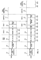
- FIGURE 2 depicts an exemplary embodiment of scheduler 180 having 24 entries (shown as rows) wherein each entry is associated with a pending Op. Each entry includes a series of fields, collectively shown as scheduling reservoir 240. for representing static and dynamic data associated with a pending Op.
- scheduler 180 provides a series of specialized logic blocks, collectively shown as control logic 230, coupled to the entries of scheduling reservoir 240 to receive data associated with pending Ops.
- the specialized logic blocks (shown as columns 231, 232, 233, 235, and 236) of control logic 230 supply signals which control the sequencing of Op execution and the supply of operands to and distribution of results from the execution units.
- Control logic 230 includes issue selection logic 231, operand selection logic 232, load-store ordering logic 234, status flag handling logic 235, and self-modifying code support logic 536.
- Issue selection logic 231 controls the selection of Ops from scheduling reservoir 240 for issue to available execution units during each cycle.
- Operand selection logic 232 identifies an appropriate source for operand data required by Ops which have been issued to execution units. Depending on data dependencies and sequencing of Ops within the execution engine 150, the appropriate source may be register file 190, a destination value field associated with another pending Op entry (destination value fields for scheduler entries are shown collectively as 250), or the result of a complete Op which is supplied on one of the result buses (shown collectively as result busses 272).
- Control signals supplied by issue selection logic 231 and operand selection logic 232 allow scheduler 180 to issue Ops from scheduling reservoir 240 to available execution units and to select the appropriate operand source for each Op issued.
- scheduler 180 issues Ops out-of-order and execution units (e.g., load unit 152, store unit 153, register unit X 154, register unit Y 155, and branch unit 158) execute Ops out-of-order, certain Op pairs must be completed in-order with respect to each other. For example, LdOps and StOps which read from and write to the same physical memory location must access memory in-order. Load-store ordering logic 234 maintains such execution ordering between LdOps and StOps.
- Self-modifying code support logic 236, which is described in greater detail below, triggers a self-modifying code fault in response to indications from store queue 159 and physical address tag fields 243.
- Store queue 159 provides several bits of the target linear and physical addresses for StOps that store queue 159 is preparing to commit.
- Self-modifying code support logic 236 compares these address bits to instruction address (or addresses, if the instructions were from different pages) stored as physical address tag fields 243 for each Op quad. If any quad matches, there may be a write to an instruction which has already been fetched or is now present (decoded) as an operation.
- self-modifying code support logic 236 signals global control logic 260 to flush scheduler 180 and the fetch/decode process is restarted from the instruction following the last committed instruction (i.e., the instruction following the instruction that modified the instruction stream).
- Scheduler 180 treats detection of self-modifying code as a trap or fault (i.e., it factors into "trap pending").
- Scheduler 180 includes a destination value field associated with each scheduler entry. Collectively these destination value fields are shown as 250. In conjunction with operand selection logic 232, destination value fields 250 implement a reorder buffer and implicit register renaming. Operand values associated with architectural registers of register file 190 are represented in destination value fields 250 and are typically supplied to execution units as register operand values via operand busses 271. However, operand values may instead be supplied from register file 190 if none of the destination value fields 250 represent a more recent register state (i.e., an as yet uncommitted register state). Results of completed Ops are supplied via result busses 272 to the destination value field of the scheduler entry associated with the completed Op. In addition, these results may also be supplied to execution units as operands for pending Ops. Results are forwarded via result busses 272.
- scheduling reservoir entry 240.1 contains information regarding an operation (Op) which is awaiting execution, which is in the process of being executed, or which is completed.
- Opera an operation
- Most of the fields of a scheduling reservoir entry are initialized when instruction decoder 130 loads a new Op into scheduling reservoir 240. However, other fields are later loaded or updated. For example, a state field (shown for each entry as field 242) is updated as the corresponding Op advances through stages of an execution pipeline.
- static fields Storage fields that retain a value from the time an Op is loaded into scheduling reservoir 240 until retired from scheduler 180 are referred to as "static fields.” Fields which can be updated with new values are referred to as “dynamic fields.” Static field data and initial data values of dynamic fields are supplied by instruction decoder 140.
- a 3-bit field, Type[2:0], of each scheduling reservoir entry (shown in FIGURE 2 as type field 241) specifies the Op type associated with the scheduling reservoir entry. Op type is particularly important for issue selection purposes (e.g., LdOps should issue to a load unit such as 150 ); however, load/store ordering control also makes use of type field 241.
- the following signals are decoded from type field 241:
- Scheduler 180 includes 24 entries in scheduling reservoir 240 and destination value fields 250 which are managed as a FIFO. Data corresponding to new Ops are loaded in at the "top,” shift toward the "bottom” as execution of progresses, and are retired from the bottom of scheduling reservoir 240. To simplify control, scheduler 180 manages scheduling reservoir 240 and destination value fields 250 on an Op quad basis. Ops are loaded into, shifted through, and retired from scheduling reservoir 240 in groups of four. In this way, scheduler granularity matches the decode bandwidth of both the emcode ROM 142 and MacDec 141 of instruction decoder 140. Scheduler 180 therefore manages 24 Op entries as six Op quad entries in a six-deep, four-wide FIFO.
- scheduling reservoir 240 can be viewed as a six-entry shift register containing Op quads.
- Each Op quad contains four Op entries, plus additional fields associated with the Op quad as a whole.
- These Op quad fields e.g., physical address tag fields 243, are supplied by instruction decoder 140.
- Physical address tag fields 243 include SmclstAddr, SmclstPg, Smc2ndAddr, and Smc2ndPg fields. Together with an Op quad valid field, OpQV, these physical address tag fields 243 provide descriptive information to self-modifying code support logic 236, which is organized with Op quad granularity. Illustratively, physical address tag fields 243.1 and self-modifying code support logic 236.1 correspond to Op quad 0 of scheduler 180. SmclstAddr and Smc1stPg represent portions of a first physical memory address for CISC instructions from which an Op (or Ops) of the associated Op quad were decoded.
- physical address tag fields 243 SmclstPg and SmclstAddr encode bits 19:12 and 11:5 (respectively) of the physical memory address for the CISC instruction associated with the first Op of the Op quad. Because the CISC instruction precursors of the Ops of an Op quad may cross cache line boundaries a second physical memory address may be necessary to fully tag an Op quad with the addresses of its associated CISC instructions. In such a case, Smc2ndAddr and Smc2ndPg represent portions of a second physical memory address for CISC instructions from which an Op (or Ops) of the associated Op quad were decoded.
- physical address tag fields 243 Smc2ndPg and Smc2ndAddr encode bits 19:12 and 11:5 (respectively) of the physical memory address for the cross-cache-line CISC instructions associated with a subsequent Op (or Ops) of the Op quad.
- Instruction decoder 140 supplies physical address tag fields 243 SmclstAddr and SmclstPg (and Smc2ndAddr and Smc2ndPg if there are CISC instructions from more than one physical memory page represented in the Op quad) to scheduling reservoir 240.
- Each entry of scheduling reservoir 240 includes fields describing outstanding Ops. These fields store static information originally derived from the Ops fetched or decoded by instruction decoder 140 and also dynamic state information resulting from Op execution or characterizing the execution pipeline status of a given Op.
- scheduler 180 is an instruction sequence-ordered array of Op state information (scheduling reservoir 240) with associated control logic 230 generating control signals to issuing Ops from the array to respective execution units, to control Op execution through sequences of pipeline stages, and to eventually retiring Ops from the scheduler.
- control logic 230 includes five specialized blocks of control logic (issue selection logic 231, operand selection logic 232, load-store ordering logic 234, status flag handling logic 235, and self-modifying code support logic 236), each having portions (illustratively portion 234.3 of load-store ordering logic 234) receiving information from corresponding entries of scheduling reservoir 240.
- Control logic blocks supply control signals to the execution units.
- load-store ordering logic 234 supplies control signals to load unit 152 and store unit 153 via control lines represented collectively as 273.
- control logic blocks of scheduling reservoir 240 depend on the state of fields in Op entries.
- the State[3:0] field indicates the progress of execution of associated operations. From a logical perspective, all state sequencing within the scheduler is single cycle in nature. State transition decisions are made each cycle based on the machine state during the cycle.
- the structure of scheduler 180 reflects the pipelined nature of Op execution. Scheduler 180 (and correspondingly each entry) can be divided into many distinct, rather independent logic portions, each of which is directly associated with a specific processing stage of a given type of operation or execution pipeline.
- FIGURE 3 shows pipeline staging for RegOps and LdStOps.
- Scheduler 180 exerts primary control over execution pipelines during the issue and operand fetch stages, 330 and 340. Processing within issue stage 330 and within operand fetch stage 340 can be broken down into two phases per stage, wherein each phase nominally occupying a half clock cycle. Issue stage 330 includes an issue selection phase and a broadcast phase, while operand fetch stage 340 includes an operand selection phase and operand forwarding phase.
- scheduler 180 selects the next Ops to enter the pipelines associated with load unit 152, store unit 153, register unit X 154, and register unit Y 155 (four Op selections occur at once).
- broadcast phase 330.2 of issue stage 330 information about each of the register operands for each selected Op is broadcast to all scheduler entries and to external logic (including register file 190 and the execution units).
- the broadcast phase 330.2 sets up to locate operand values which may reside in one of the destination value fields 250 of scheduler 180 or in register file 190, or which may correspond to results to be produced on result busses 272 one of the execution units (e.g., load unit 152, store unit 153 , or register units 154 and 155).
- the execution units e.g., load unit 152, store unit 153 , or register units 154 and 155.
- scheduler 180 locates up to eight operand values (4 Ops * 2 operands/Op) and determines the status of each operand value, i.e., whether a valid value is in fact available from the designated source. Based on this information, scheduler 180 determines which of the Ops in operand fetch stage 0 (stage 340) will advance into their respective execution pipes, i.e., into stage 1 (stage 350), following the operand forward phase. Advancement decisions are made independently for each Op and only operand dependencies need constrain the order with which operations are actually executed. Absent such data dependencies, Ops which issue to different execution units are generally processed through their respective pipelines in arbitrary order with respect to those Ops assigned to other execution units. One exception to this general rule involves the respective ordering of loads and stores (i.e., of LdOps and StOps) and is in greater detail discussed below.
- the first two scheduler-related stages, the "operand issue” stage 330 and the "operand fetch” stage 340 are common to RegOps and LdStOps. Subsequent stages are the execution stages. RegOps include a single execution stage 350 because all RegOps execute in a single cycle. Furthermore, once a RegOp enters the execution stage, it always successfully completes and exits stage 350 at the end of that clock cycle. LdStOps, on the other hand, have two execution stages 352 and 360, during which address calculation, segment and page translation (and protection checking), and data cache accessing (in the case of LdOps) all take place.
- LdStOps can be held up for arbitrary periods of time in either stage 360 or 370 . Most hold ups appear in the second stage 370. Most commonly, hold ups in stage 370 result from data cache 170 misses, data TLB 171 misses, and page faults. Hold ups in stage 360 result from misaligned memory references and from stage 370 being occupied and blocked by an LdStOp not advancing to completion.
- scheduler 180 transfers operand values from the designated sources via operand busses and/or result busses shown collectively in FIGURE 2 as busses 271 and 272 to execution units such as load unit 152, store unit 153, register unit X 154, and register unit Y 155.
- the exemplary embodiment includes nine operand busses 271, eight of which provide operand values for operations in stage 0.
- operand transfers occur regardless of whether values are valid, thereby simplifying control logic. If an operand value is invalid, it is ignored by the respective execution unit because the scheduler 180 does not advance the associated operation to stage 1.
- Immediate values for RegOps are handled as part of the register operand forwarding mechanism described above. In such cases, the immediate value is forwarded directly from the particular one of the destination value fields 250 of the scheduler 180 entries associated with the Op.
- Displacement values are also transferred during operand forward phase 340.2, via displacement busses 189.4, to load unit 152 and store unit 153 (independent values to each unit). These displacements are 32-bit values and always come from the entries of scheduler 180. The selection of the source entry occurs during operand selection phase 340.1. When a LdOp or a StOp enters stage 1. load unit 152 and store unit 153 latch associated displacement and operand values.
- Scheduler 180 implements the four-phase control mechanism (as described above) for providing the address operands and displacement; however, StOps require a store data operand in addition to address operands and displacement values.
- Scheduler 180 performs a four-phase process for obtaining the store data for a StOp.
- the StOp data obtaining process is similar to that described above; however the store data is obtained during execution stage 2 (370).
- the process for providing the store data is synchronized with stages 1 and 2 of the StOp and includes a selection phase 390.1 identifying the StOp in execution stage 1, a broadcast phase 390.2 transmitting information describing the source of a data operand, a data operand selection phase 390.3, and an data operand forwarding phase 390.4.
- Store data is fetched in parallel with StOp execution; and the actual data value is obtained and provided to store queue 159 upon completion of StOp processing. If a valid store data value is not available, the StOp is held up in stage 2.
- RegOps and LdOps complete by storing results to one of the destination value fields 250 of scheduler 180.
- Each of the destination value fields 250 is associated with an Op entry and is used as a temporary store (a reorder buffer) for values which may eventually be committed to register file 190 by OCU 265.
- the corresponding temporary store before commitment to memory is store queue 159.
- Store queue 159 buffers memory writes associated with a StOp in a first commit stage until OCU 265 releases the memory write to a second commit stage.
- Register, flag, and memory state changes associated with completed Ops are committed (or made permanent) by OCU (Operation Commit Unit) 265.
- OCU 265 then retires the corresponding Op entry from scheduler 180.
- state changes can result from the execution of an Op.
- the principal types of state changes are abortable and include: general register changes; status flag changes; and memory writes.
- General register changes result from all RegOps, LdOps, LIMM Ops, LDKxx operations, and STUPD StOps.
- Status flag changes result from ".cc" RegOps, and memory writes result STxxx StOps.
- Scheduler 180 and store queue 159 support abortable state changes through the general technique of temporarily storing register and status results in the destination value fields 250 and scheduling reservoir 240 of scheduler 180 and by storing memory write data in store queue 159. Temporary (or speculative) register values, status values, and memory write values are held until the associated Ops are committed and retired by OCU 265. Scheduler 180 speculatively supplies register values. status values, and memory write values residing in scheduling reservoir 240 and store queue 159 to dependent Ops as necessary. However, permanent state changes to register file 190 and to the memory address space (distributed among data cache 170, instruction cache 130, an L2 cache, and main memory) are made during Op commitment.
- OCU 265 examines each of the Op entries within the bottom Op quad entry and tries to commit the results of as many of these operations as possible.
- the state changes associated with the four Ops of an Op quad may be committed in one cycle or over many cycles. If all the Ops of an Op quad have been committed or are being successfully committed, the Op quad is retired from scheduler 180 at the end of the current cycle. Otherwise, as many state changes as possible are committed and the process is repeated during successive cycles until all state changes have been committed.
- OCU 265 manages and controls the commitment of memory write data values associated with StOps to the memory address space, i.e., to locations in the L1 cache (data cache 170 and instruction cache 130), an L2 cache, and main memory.
- Memory write commitment involves an associated store queue 159 entry and at most one memory write is committed by OCU 265 per cycle.
- OCU 265 scans scheduling reservoir 240 field values for Op entries in the bottom two Op quad to identify StOps with memory writes to commit.
- OCU 265 During each cycle. OCU 265 's memory write commit logic searches the bottom two Op quad entries of scheduler 180 for the next/oldest uncommitted memory-writing StOp (i.e. for the next StOp and associated store queue 159 entry to try and commit). Since scheduler 180 and store queue 159 are both managed as FIFOs, the Op entry selected by OCU 265 must be associated with the bottom/oldest entry of store queue 159.
- the StOp (memory write) commitment process is implemented as a two-stage commit pipeline. During the first commit stage, no control decisions are made. Instead, OCU 265 triggers a data cache tag lookup for the store queue 159 entry associated with the next/oldest uncommitted memory-writing StOp in scheduler 180. The accessed tag data is simply latched for examination during the second commit stage. Data cache 170 tag lookup is performed "blindly," i.e., without consideration for whether the associated StOp is presently committable. In the exemplary embodiment, OCU 265 selects an Op entry from scheduler 180 and store queue 159 concurrently presents the memory write address for the associated store queue 159 entry to data cache 170 (i.e., initiates a tag lookup).
- a write commit is able to advance into commit stage 2 when that stage is either empty or is successfully completing the commitment of a write.
- the associated Stop can be retired from scheduler 180.
- OCU 265 determines whether the selected StOp is committable, i.e., whether:
- the write commit pipeline of store queue 159 is one write wide and therefore supports the commitment of only one memory-writing StOp per cycle. For Op quads which containing no more than one memory-writing StOp, this allows the possible commitment and retirement of one Op quad per cycle. However, for Op quads containing two, three, or four such StOps, a corresponding minimum number of cycles is required to commit the each Stop entry of the Op quad. As a result such an Op quad remains at the bottom of scheduler 180 for at least the corresponding number of cycles.
- OPO is the oldest Op and OP3 is the youngest Op in the bottom/last Op quad of scheduler 180.
- OP4-OP7 are the corresponding Ops in the second to last Op quad of scheduler 180 and OP8-OP11 are the corresponding Ops in the third to last Op quad of scheduler 180.
- the operation of OCU 265 is based on a set of mask bits (CmtMask[7:0]) which represent the OCU 265 's progress in committing memory-writing StOps from the last two Op quad.
- the first N-bits (starting from bit 0) of CmtMask [7:0] are clear indicating that OCU 265 has committed any StOps up to the Nth such Op position, which contains the next StOp to be committed. All Ops corresponding to the remaining, set mask bits of CmtMask [7:0] have yet to be examined for committable Stops. OCU 265 also maintains a set of bits (UncmtStOp[7:0]) indicating which Op positions contain uncommitted memory-writing StOps.
- OCU 265 selects the next uncommitted StOp and generates a new set of mask bits based on the position of the selected StOp.
- the unmasked Ops are examined to determine whether the selected StOp is presently committable or an abort cycle needs to be initiated. In the former case, if the selected StOp is committable and if stage 2 of the commit pipe is able to accept a new write commit at the end of the cycle, OCU 265 commits the StOp and updates the UncmtStOp bits. OCU 265 also shifts the bits of UncmtStOp to match any shifting of the last two Op quads.
- Memory writes are committed to the address space (i.e., to data cache 170, to instruction cache 130, to an L2 cache, and/or to main memory) in phase 2 382.2 of LdStOp commitment stage 382. Since load-store ordering logic 234 enforces execution ordering between LdOps and StOps which access the same memory address, a younger load is guaranteed to return the just-committed memory write data. However, if the memory write committed in phase 2 382.2 of LdStOp commitment stage 382 stores into the instruction stream, younger Ops (and their precursor x86 instructions) in various pipeline stages (i.e., x86 instruction fetch stage 310, x86 instruction decode stage 320, issue stage 330, operand fetch stage 340, execution stages 351.
- stage 1 459 of store queue 159 provides portions of the linear and physical address (i.e., the StOp address) for memory write data which the store queue 159 is preparing to commit in stage 2 460.
- stage 1 459 of store queue 159 provides bits 11-5 of the linear address STQ_LinAddr (11,5) and bits 19-12 of the physical address STQ_PhysAddr(19,12).
- Self-modifying code support logic 236 of scheduler 180 receives the StOp address and compares it against respective physical address tags Smc1stAddr, Smc1stPg, Smc2ndAddr, and Smc2ndPg stored in Op quad fields 443.1, 443.2, 443.3, and 443.4 of scheduling reservoir 240. Based on this comparison, self-modifying code support logic 236 determines whether the StOp being committed by store queue 159 writes to an address covered by any Op quad in scheduler 180. If so, self-modifying code support logic 236 triggers a Self-Modifying Code (SMC) trap.
- SMC Self-Modifying Code
- instruction decoder 140 supplies the contents of Op quad fields 443.1, 443.2, 443.3, and 443.4 (collectively shown in FIGURE 2 as physical address tag fields 243) as Ops are issued to scheduler 180.
- the physical address tags Smc1stAddr, Smc1stPg, Smc2ndAddr, and Smc2ndPg stored in Op quad fields 443.1, 443.2, 443.3, and 443.4 represent bits 19-5 of the first and second physical memory addresses for x86 instructions from which Ops of the corresponding Op quad were decoded.
- Two physical memory addresses are required when the Ops of the corresponding Op quad were decoded from an x86 instruction (or instructions) which cross a cache line boundary.
- Instruction decoder 140 also traps self-modifying code using physical address tags.
- address match logic 444 and fetch control logic 447 of instruction decoder 140 receive portions of the linear and physical address (i.e., the StOp address) for the memory write which the store queue 159 is preparing to commit in stage 2 460.
- stage 1 459 of store queue 159 provides bits 11-5 of the linear address STQ_LinAddr (11,5) and bits 19-12 of the physical address STQ_PhysAddr (19, 12).
- Address match logic 444 compares the StOp address against address tags 446 respectively associated with entries in instruction buffer 445. If a match is found, address match logic 444 triggers an SMC trap.
- Global control logic 260 flushes instruction decoder 140 and the fetch/decode process is restarted from the last committed instruction.
- an SMC trap is handled as follows. After all Ops associated with the triggering StOp are committed (i.e., the set of Ops decoded from the same x86 instruction as the triggering StOp or the entire Op quad in which the triggering StOp is a member, whichever is larger), Ops associated with subsequent x86 instructions are aborted.
- the following emcode implements an SMC trap: The SMC trap emcode obtains the Extended Instruction Pointer (EIP) of the above aborted instruction. The SMC trap emcode then waits until the triggering StOp is acknowledged by the memory subsystem.
- EIP Extended Instruction Pointer
- the triggering StOp could instead be acknowledged by the L2 cache.
- an acknowledgment means that a snoop to instruction cache 130 has already been issued.
- the SMC trap emcode After the SMC trap emcode has synchronized with the memory write associated with the triggering Stop, it then jumps back (doing a WrIP) to fetch the next x86 instruction in the instruction stream. At this point it is guaranteed that the next bytes fetched from main memory (or alternatively from the L2 cache) will be up to date.
- fetch control logic 447 of instruction decoder 140 stores a copy of the physical address (i.e., the StOp address) associated with the committed memory write. Whenever instruction decoder 140 fetches new instruction bytes from instruction cache 130, fetch control logic 447 checks the current fetch address against its stored copy of StOp address for the last-committed memory write. If the current fetch address matches with the stored copy of the StOp address, then fetch control logic 447 nullifies the fetch.
- Fetch control logic 447 of instruction decoder 140 continues to reissue the same fetch address until the committed StOp is acknowledged by the memory subsystem.
- fetch control logic 447 receives an acknowledgment from the memory subsystem, it clears its StOp address store.
- the acknowledgment could be supplied instead by the L2 cache.
- the memory subsystem issues a snoop to instruction cache 130 before or (at the latest) concurrent with its StOp acknowledgment. While the instruction cache 130 is processing a snoop, it inhibits the processing of fetches from instruction decoder 140. By inhibiting fetches during snoop processing, instruction cache 130 closes a second short window during which instruction fetches could potentially return stale bytes.
- Each Op quad of scheduler 180 may contain bytes of decoded x86 instructions spanning two lines of instruction cache 130.
- an entry in instruction buffer 445 may span two lines of instruction cache 130.
- a line in the instruction decoder 140 is 32 bytes. This means that the physical address tags associated with each Op quad entry of scheduler 180 and with each entry of instruction buffer 445 need to encode addresses for both possible 32-byte cache lines.
- address tags 446 and physical address tag fields 243 a pair of complete physical addresses tags (bits 31:5) is stored for each Op quad entry of scheduler 180 and for each entry of instruction buffer 445.
- address tags 446 and physical address tag fields 243 store partial physical addresses, each containing bits 19:5 of the physical memory address of the associated x86 instruction (or instructions).
- the exemplary embodiment supports single-cycle throughput of writes to memory.
- the data cache 170 is a write-back cache.
- a memory write commitment associated with a StOp hits in data cache 170 and the line is found to be Owned or Dirty, then the write can be processed at a rate of 1 per-cycle.
- This situation presents some difficulty with respect to handling self-modifying code if an Owned/Dirty line is allowed to reside in both the data cache 170 and instruction cache 130.
- instruction cache 130 would have to be snooped immediately with the StOp being committed, which would add complexity since contention issues arise in access instruction cache 130 tag RAM.
- a dedicated address bus (not shown) would have to be sent from the data cache 170 to the instruction cache 130.
- cache control logic 160 prevents a cache line from residing in both caches at the same time in the exemplary embodiment.
- the estimated performance impact of this restriction is negligible.
- Op entries in scheduler 180 as Op quads are merely illustrative.
- Alternative embodiments may incorporate other structures and/or methods for representing the nature and state of operations in a computer having multiple and/or pipelined execution units.
- alternative embodiments may incorporate different hierarchies of memories and caches. for example L1 and L2 caches. In such alternative embodiments, store acknowledgments may be provided by an L2 cache.
- Alternative embodiments may provide for a different distribution of structures and functionality, including structures for tag representation and comparison, among the scheduler 180, the store unit 153, the store queue 159. and the instruction decoder 140. Additionally, structures and functionality presented as hardware in the exemplary embodiment may be implemented as software, firmware, or microcode in alternative embodiments. A wide variety of computer system configurations are envisioned, each embodying self-modifying code handling in accordance with the present invention.
- such a computer system includes a processor 100 providing self-modifying code handling in accordance with the present invention, a memory subsystem (e.g., RAM 1020), a display adapter 1010, disk controller/adapter 1030, various input/output interfaces and adapters (e.g., parallel interface 1009, serial interface 1008, LAN adapter 1007, etc.), and corresponding external devices (e.g., display device 1001, printer 1002, modem 1003, keyboard 1006, and data storage).
- Data storage includes such devices as hard disk 1032, floppy disk 1031, a tape unit, a CD-ROM, a jukebox, a redundant array of inexpensive disks (RAID), a flash memory, etc.
Landscapes
- Engineering & Computer Science (AREA)
- Software Systems (AREA)
- Theoretical Computer Science (AREA)
- Physics & Mathematics (AREA)
- General Engineering & Computer Science (AREA)
- General Physics & Mathematics (AREA)
- Advance Control (AREA)
- Memory System Of A Hierarchy Structure (AREA)
- Executing Machine-Instructions (AREA)
Applications Claiming Priority (7)
| Application Number | Priority Date | Filing Date | Title |
|---|---|---|---|
| US506995P | 1995-10-06 | 1995-10-06 | |
| US5069P | 1995-10-06 | ||
| US502195P | 1995-10-10 | 1995-10-10 | |
| US5021P | 1995-10-10 | ||
| US08/592,150 US5826073A (en) | 1995-10-06 | 1996-01-26 | Self-modifying code handling system |
| PCT/US1996/015420 WO1997013198A1 (en) | 1995-10-06 | 1996-10-03 | Self-modifying code handling system |
| US592150 | 2000-06-12 |
Publications (2)
| Publication Number | Publication Date |
|---|---|
| EP0853785A1 EP0853785A1 (en) | 1998-07-22 |
| EP0853785B1 true EP0853785B1 (en) | 2001-05-23 |
Family
ID=27357779
Family Applications (1)
| Application Number | Title | Priority Date | Filing Date |
|---|---|---|---|
| EP96933906A Expired - Lifetime EP0853785B1 (en) | 1995-10-06 | 1996-10-03 | Self-modifying code handling system |
Country Status (6)
| Country | Link |
|---|---|
| US (1) | US5826073A (enExample) |
| EP (1) | EP0853785B1 (enExample) |
| JP (1) | JP3720370B2 (enExample) |
| AU (1) | AU7246396A (enExample) |
| DE (1) | DE69612991T2 (enExample) |
| WO (1) | WO1997013198A1 (enExample) |
Cited By (1)
| Publication number | Priority date | Publication date | Assignee | Title |
|---|---|---|---|---|
| CN104951276A (zh) * | 2015-06-24 | 2015-09-30 | 福州瑞芯微电子有限公司 | 一种芯片指令高速缓存失效的检测方法及系统 |
Families Citing this family (29)
| Publication number | Priority date | Publication date | Assignee | Title |
|---|---|---|---|---|
| US5758349A (en) * | 1995-12-27 | 1998-05-26 | International Business Machines Corporation | Process and system for run-time inheritance and disinheritance of methods and data |
| US6009516A (en) * | 1996-10-21 | 1999-12-28 | Texas Instruments Incorporated | Pipelined microprocessor with efficient self-modifying code detection and handling |
| US6170055B1 (en) | 1997-11-03 | 2001-01-02 | Iomega Corporation | System for computer recovery using removable high capacity media |
| US7941647B2 (en) | 1999-01-28 | 2011-05-10 | Ati Technologies Ulc | Computer for executing two instruction sets and adds a macroinstruction end marker for performing iterations after loop termination |
| US8074055B1 (en) | 1999-01-28 | 2011-12-06 | Ati Technologies Ulc | Altering data storage conventions of a processor when execution flows from first architecture code to second architecture code |
| US8065504B2 (en) | 1999-01-28 | 2011-11-22 | Ati International Srl | Using on-chip and off-chip look-up tables indexed by instruction address to control instruction execution in a processor |
| US8127121B2 (en) | 1999-01-28 | 2012-02-28 | Ati Technologies Ulc | Apparatus for executing programs for a first computer architechture on a computer of a second architechture |
| US6671665B1 (en) * | 1999-02-19 | 2003-12-30 | Texas Instruments Incorporated | Emulation system with search and identification of optional emulation peripherals |
| US6850647B1 (en) * | 1999-07-30 | 2005-02-01 | Michael L. Gough | System, method and article of manufacture for decompressing digital camera sensor data |
| JP3739607B2 (ja) * | 1999-08-24 | 2006-01-25 | 富士通株式会社 | 情報処理装置 |
| US6629175B1 (en) * | 2000-04-14 | 2003-09-30 | International Business Machines Corporation | Efficient adapter context switching |
| US7360028B1 (en) * | 2000-05-05 | 2008-04-15 | Sun Microsystems, Inc. | Explicit store-to-instruction-space instruction for self-modifying code and ensuring memory coherence between instruction cache and shared memory using a no-snoop protocol |
| US6807623B2 (en) * | 2000-07-27 | 2004-10-19 | Matsushita Electric Industrial Co., Ltd. | Data processing control system, controller, data processing control method, program, and medium |
| US20030093775A1 (en) * | 2001-11-14 | 2003-05-15 | Ronald Hilton | Processing of self-modifying code under emulation |
| US6543034B1 (en) * | 2001-11-30 | 2003-04-01 | Koninklijke Philips Electronics N.V. | Multi-environment testing with a responder |
| US7251594B2 (en) * | 2001-12-21 | 2007-07-31 | Hitachi, Ltd. | Execution time modification of instruction emulation parameters |
| US7260217B1 (en) * | 2002-03-01 | 2007-08-21 | Cavium Networks, Inc. | Speculative execution for data ciphering operations |
| CA2418255A1 (en) * | 2003-01-31 | 2004-07-31 | Ibm Canada Limited - Ibm Canada Limitee | Tracking and maintaining related and derivative code |
| US20040163082A1 (en) * | 2003-02-13 | 2004-08-19 | Marc Tremblay | Commit instruction to support transactional program execution |
| US7711990B1 (en) * | 2005-12-13 | 2010-05-04 | Nvidia Corporation | Apparatus and method for debugging a graphics processing unit in response to a debug instruction |
| US8516229B2 (en) * | 2010-02-05 | 2013-08-20 | International Business Machines Corporation | Two pass test case generation using self-modifying instruction replacement |
| US9436476B2 (en) | 2013-03-15 | 2016-09-06 | Soft Machines Inc. | Method and apparatus for sorting elements in hardware structures |
| US20140281116A1 (en) | 2013-03-15 | 2014-09-18 | Soft Machines, Inc. | Method and Apparatus to Speed up the Load Access and Data Return Speed Path Using Early Lower Address Bits |
| US9747212B2 (en) * | 2013-03-15 | 2017-08-29 | International Business Machines Corporation | Virtual unifed instruction and data caches including storing program instructions and memory address in CAM indicated by store instruction containing bit directly indicating self modifying code |
| US9582322B2 (en) | 2013-03-15 | 2017-02-28 | Soft Machines Inc. | Method and apparatus to avoid deadlock during instruction scheduling using dynamic port remapping |
| US9627038B2 (en) | 2013-03-15 | 2017-04-18 | Intel Corporation | Multiport memory cell having improved density area |
| US9946538B2 (en) * | 2014-05-12 | 2018-04-17 | Intel Corporation | Method and apparatus for providing hardware support for self-modifying code |
| US9996329B2 (en) | 2016-02-16 | 2018-06-12 | Microsoft Technology Licensing, Llc | Translating atomic read-modify-write accesses |
| US9986200B1 (en) * | 2017-05-11 | 2018-05-29 | Novatek Microelectronics Corp. | Method and video conversion system of updating video setting |
Family Cites Families (4)
| Publication number | Priority date | Publication date | Assignee | Title |
|---|---|---|---|---|
| EP0159712B1 (en) * | 1984-04-27 | 1991-01-30 | Bull HN Information Systems Inc. | Control means in a digital computer |
| US5226130A (en) * | 1990-02-26 | 1993-07-06 | Nexgen Microsystems | Method and apparatus for store-into-instruction-stream detection and maintaining branch prediction cache consistency |
| US5692167A (en) * | 1992-07-31 | 1997-11-25 | Intel Corporation | Method for verifying the correct processing of pipelined instructions including branch instructions and self-modifying code in a microprocessor |
| US5434987A (en) * | 1993-09-21 | 1995-07-18 | Intel Corporation | Method and apparatus for preventing incorrect fetching of an instruction of a self-modifying code sequence with dependency on a bufered store |
-
1996
- 1996-01-26 US US08/592,150 patent/US5826073A/en not_active Expired - Lifetime
- 1996-10-03 JP JP51432797A patent/JP3720370B2/ja not_active Expired - Lifetime
- 1996-10-03 DE DE69612991T patent/DE69612991T2/de not_active Expired - Lifetime
- 1996-10-03 WO PCT/US1996/015420 patent/WO1997013198A1/en not_active Ceased
- 1996-10-03 EP EP96933906A patent/EP0853785B1/en not_active Expired - Lifetime
- 1996-10-03 AU AU72463/96A patent/AU7246396A/en not_active Abandoned
Cited By (2)
| Publication number | Priority date | Publication date | Assignee | Title |
|---|---|---|---|---|
| CN104951276A (zh) * | 2015-06-24 | 2015-09-30 | 福州瑞芯微电子有限公司 | 一种芯片指令高速缓存失效的检测方法及系统 |
| CN104951276B (zh) * | 2015-06-24 | 2017-05-31 | 福州瑞芯微电子股份有限公司 | 一种芯片指令高速缓存失效的检测方法及系统 |
Also Published As
| Publication number | Publication date |
|---|---|
| EP0853785A1 (en) | 1998-07-22 |
| JP3720370B2 (ja) | 2005-11-24 |
| AU7246396A (en) | 1997-04-28 |
| DE69612991D1 (de) | 2001-06-28 |
| WO1997013198A1 (en) | 1997-04-10 |
| JP2001517333A (ja) | 2001-10-02 |
| US5826073A (en) | 1998-10-20 |
| DE69612991T2 (de) | 2002-01-17 |
Similar Documents
| Publication | Publication Date | Title |
|---|---|---|
| EP0853785B1 (en) | Self-modifying code handling system | |
| EP0853784B1 (en) | Out-of-order load/store execution control | |
| US5835747A (en) | Hierarchical scan logic for out-of-order load/store execution control | |
| JP4578042B2 (ja) | 接近して結合される多重プロセッサのための高速マルチスレッディング | |
| US5751983A (en) | Out-of-order processor with a memory subsystem which handles speculatively dispatched load operations | |
| JP3977016B2 (ja) | 仮想レジスタ番号を用いて論理レジスタ番号を物理レジスタ番号にマッピングするように構成されるプロセッサ | |
| US6021485A (en) | Forwarding store instruction result to load instruction with reduced stall or flushing by effective/real data address bytes matching | |
| US5721855A (en) | Method for pipeline processing of instructions by controlling access to a reorder buffer using a register file outside the reorder buffer | |
| US5557763A (en) | System for handling load and/or store operations in a superscalar microprocessor | |
| EP0686914B1 (en) | Resynchronisation of a superscalar processor | |
| US5867683A (en) | Method of operating a high performance superscalar microprocessor including a common reorder buffer and common register file for both integer and floating point operations | |
| US6963967B1 (en) | System and method for enabling weak consistent storage advantage to a firmly consistent storage architecture | |
| US6609192B1 (en) | System and method for asynchronously overlapping storage barrier operations with old and new storage operations | |
| US5664137A (en) | Method and apparatus for executing and dispatching store operations in a computer system | |
| US20020087849A1 (en) | Full multiprocessor speculation mechanism in a symmetric multiprocessor (smp) System | |
| JPH07334364A (ja) | スーパースカラマイクロプロセッサおよびropを処理する方法 | |
| US5745724A (en) | Scan chain for rapidly identifying first or second objects of selected types in a sequential list | |
| US6725340B1 (en) | Mechanism for folding storage barrier operations in a multiprocessor system | |
| US7213133B2 (en) | Method and apparatus for avoiding write-after-write hazards in an execute-ahead processor | |
| JP3866920B2 (ja) | 命令のリタイアメント時に物理レジスタを選択的に自由にするよう構成されたプロセッサ | |
| US6038657A (en) | Scan chains for out-of-order load/store execution control | |
| US20050223201A1 (en) | Facilitating rapid progress while speculatively executing code in scout mode | |
| US6175909B1 (en) | Forwarding instruction byte blocks to parallel scanning units using instruction cache associated table storing scan block boundary information for faster alignment | |
| EP0912927B1 (en) | A load/store unit with multiple pointers for completing store and load-miss instructions | |
| EP0912930B1 (en) | A functional unit with a pointer for mispredicted branch resolution, and a superscalar microprocessor employing the same |
Legal Events
| Date | Code | Title | Description |
|---|---|---|---|
| PUAI | Public reference made under article 153(3) epc to a published international application that has entered the european phase |
Free format text: ORIGINAL CODE: 0009012 |
|
| 17P | Request for examination filed |
Effective date: 19980401 |
|
| AK | Designated contracting states |
Kind code of ref document: A1 Designated state(s): DE ES FR GB NL |
|
| GRAG | Despatch of communication of intention to grant |
Free format text: ORIGINAL CODE: EPIDOS AGRA |
|
| 17Q | First examination report despatched |
Effective date: 20000830 |
|
| GRAG | Despatch of communication of intention to grant |
Free format text: ORIGINAL CODE: EPIDOS AGRA |
|
| GRAH | Despatch of communication of intention to grant a patent |
Free format text: ORIGINAL CODE: EPIDOS IGRA |
|
| GRAH | Despatch of communication of intention to grant a patent |
Free format text: ORIGINAL CODE: EPIDOS IGRA |
|
| GRAA | (expected) grant |
Free format text: ORIGINAL CODE: 0009210 |
|
| AK | Designated contracting states |
Kind code of ref document: B1 Designated state(s): DE ES FR GB NL |
|
| PG25 | Lapsed in a contracting state [announced via postgrant information from national office to epo] |
Ref country code: NL Free format text: LAPSE BECAUSE OF FAILURE TO SUBMIT A TRANSLATION OF THE DESCRIPTION OR TO PAY THE FEE WITHIN THE PRESCRIBED TIME-LIMIT Effective date: 20010523 |
|
| REF | Corresponds to: |
Ref document number: 69612991 Country of ref document: DE Date of ref document: 20010628 |
|
| ET | Fr: translation filed | ||
| NLV1 | Nl: lapsed or annulled due to failure to fulfill the requirements of art. 29p and 29m of the patents act | ||
| PG25 | Lapsed in a contracting state [announced via postgrant information from national office to epo] |
Ref country code: ES Free format text: LAPSE BECAUSE OF FAILURE TO SUBMIT A TRANSLATION OF THE DESCRIPTION OR TO PAY THE FEE WITHIN THE PRESCRIBED TIME-LIMIT Effective date: 20011130 |
|
| REG | Reference to a national code |
Ref country code: GB Ref legal event code: IF02 |
|
| PLBE | No opposition filed within time limit |
Free format text: ORIGINAL CODE: 0009261 |
|
| STAA | Information on the status of an ep patent application or granted ep patent |
Free format text: STATUS: NO OPPOSITION FILED WITHIN TIME LIMIT |
|
| 26N | No opposition filed | ||
| PGFP | Annual fee paid to national office [announced via postgrant information from national office to epo] |
Ref country code: FR Payment date: 20131009 Year of fee payment: 18 |
|
| REG | Reference to a national code |
Ref country code: FR Ref legal event code: ST Effective date: 20150630 |
|
| PG25 | Lapsed in a contracting state [announced via postgrant information from national office to epo] |
Ref country code: FR Free format text: LAPSE BECAUSE OF NON-PAYMENT OF DUE FEES Effective date: 20141031 |
|
| PGFP | Annual fee paid to national office [announced via postgrant information from national office to epo] |
Ref country code: GB Payment date: 20150930 Year of fee payment: 20 |
|
| PGFP | Annual fee paid to national office [announced via postgrant information from national office to epo] |
Ref country code: DE Payment date: 20150929 Year of fee payment: 20 |
|
| REG | Reference to a national code |
Ref country code: DE Ref legal event code: R071 Ref document number: 69612991 Country of ref document: DE |
|
| REG | Reference to a national code |
Ref country code: GB Ref legal event code: PE20 Expiry date: 20161002 |
|
| PG25 | Lapsed in a contracting state [announced via postgrant information from national office to epo] |
Ref country code: GB Free format text: LAPSE BECAUSE OF EXPIRATION OF PROTECTION Effective date: 20161002 |