EP0853306B1 - Method of reducing peak current in a plasma display panel - Google Patents
Method of reducing peak current in a plasma display panel Download PDFInfo
- Publication number
- EP0853306B1 EP0853306B1 EP98100080A EP98100080A EP0853306B1 EP 0853306 B1 EP0853306 B1 EP 0853306B1 EP 98100080 A EP98100080 A EP 98100080A EP 98100080 A EP98100080 A EP 98100080A EP 0853306 B1 EP0853306 B1 EP 0853306B1
- Authority
- EP
- European Patent Office
- Prior art keywords
- data
- pulse
- electrodes
- scanning
- pixels
- Prior art date
- Legal status (The legal status is an assumption and is not a legal conclusion. Google has not performed a legal analysis and makes no representation as to the accuracy of the status listed.)
- Expired - Lifetime
Links
Images



Classifications
-
- G—PHYSICS
- G09—EDUCATION; CRYPTOGRAPHY; DISPLAY; ADVERTISING; SEALS
- G09G—ARRANGEMENTS OR CIRCUITS FOR CONTROL OF INDICATING DEVICES USING STATIC MEANS TO PRESENT VARIABLE INFORMATION
- G09G3/00—Control arrangements or circuits, of interest only in connection with visual indicators other than cathode-ray tubes
- G09G3/20—Control arrangements or circuits, of interest only in connection with visual indicators other than cathode-ray tubes for presentation of an assembly of a number of characters, e.g. a page, by composing the assembly by combination of individual elements arranged in a matrix no fixed position being assigned to or needed to be assigned to the individual characters or partial characters
- G09G3/22—Control arrangements or circuits, of interest only in connection with visual indicators other than cathode-ray tubes for presentation of an assembly of a number of characters, e.g. a page, by composing the assembly by combination of individual elements arranged in a matrix no fixed position being assigned to or needed to be assigned to the individual characters or partial characters using controlled light sources
- G09G3/28—Control arrangements or circuits, of interest only in connection with visual indicators other than cathode-ray tubes for presentation of an assembly of a number of characters, e.g. a page, by composing the assembly by combination of individual elements arranged in a matrix no fixed position being assigned to or needed to be assigned to the individual characters or partial characters using controlled light sources using luminous gas-discharge panels, e.g. plasma panels
- G09G3/288—Control arrangements or circuits, of interest only in connection with visual indicators other than cathode-ray tubes for presentation of an assembly of a number of characters, e.g. a page, by composing the assembly by combination of individual elements arranged in a matrix no fixed position being assigned to or needed to be assigned to the individual characters or partial characters using controlled light sources using luminous gas-discharge panels, e.g. plasma panels using AC panels
- G09G3/298—Control arrangements or circuits, of interest only in connection with visual indicators other than cathode-ray tubes for presentation of an assembly of a number of characters, e.g. a page, by composing the assembly by combination of individual elements arranged in a matrix no fixed position being assigned to or needed to be assigned to the individual characters or partial characters using controlled light sources using luminous gas-discharge panels, e.g. plasma panels using AC panels using surface discharge panels
-
- G—PHYSICS
- G09—EDUCATION; CRYPTOGRAPHY; DISPLAY; ADVERTISING; SEALS
- G09G—ARRANGEMENTS OR CIRCUITS FOR CONTROL OF INDICATING DEVICES USING STATIC MEANS TO PRESENT VARIABLE INFORMATION
- G09G3/00—Control arrangements or circuits, of interest only in connection with visual indicators other than cathode-ray tubes
- G09G3/20—Control arrangements or circuits, of interest only in connection with visual indicators other than cathode-ray tubes for presentation of an assembly of a number of characters, e.g. a page, by composing the assembly by combination of individual elements arranged in a matrix no fixed position being assigned to or needed to be assigned to the individual characters or partial characters
- G09G3/22—Control arrangements or circuits, of interest only in connection with visual indicators other than cathode-ray tubes for presentation of an assembly of a number of characters, e.g. a page, by composing the assembly by combination of individual elements arranged in a matrix no fixed position being assigned to or needed to be assigned to the individual characters or partial characters using controlled light sources
- G09G3/28—Control arrangements or circuits, of interest only in connection with visual indicators other than cathode-ray tubes for presentation of an assembly of a number of characters, e.g. a page, by composing the assembly by combination of individual elements arranged in a matrix no fixed position being assigned to or needed to be assigned to the individual characters or partial characters using controlled light sources using luminous gas-discharge panels, e.g. plasma panels
- G09G3/288—Control arrangements or circuits, of interest only in connection with visual indicators other than cathode-ray tubes for presentation of an assembly of a number of characters, e.g. a page, by composing the assembly by combination of individual elements arranged in a matrix no fixed position being assigned to or needed to be assigned to the individual characters or partial characters using controlled light sources using luminous gas-discharge panels, e.g. plasma panels using AC panels
- G09G3/291—Control arrangements or circuits, of interest only in connection with visual indicators other than cathode-ray tubes for presentation of an assembly of a number of characters, e.g. a page, by composing the assembly by combination of individual elements arranged in a matrix no fixed position being assigned to or needed to be assigned to the individual characters or partial characters using controlled light sources using luminous gas-discharge panels, e.g. plasma panels using AC panels controlling the gas discharge to control a cell condition, e.g. by means of specific pulse shapes
- G09G3/293—Control arrangements or circuits, of interest only in connection with visual indicators other than cathode-ray tubes for presentation of an assembly of a number of characters, e.g. a page, by composing the assembly by combination of individual elements arranged in a matrix no fixed position being assigned to or needed to be assigned to the individual characters or partial characters using controlled light sources using luminous gas-discharge panels, e.g. plasma panels using AC panels controlling the gas discharge to control a cell condition, e.g. by means of specific pulse shapes for address discharge
- G09G3/2932—Addressed by writing selected cells that are in an OFF state
-
- G—PHYSICS
- G09—EDUCATION; CRYPTOGRAPHY; DISPLAY; ADVERTISING; SEALS
- G09G—ARRANGEMENTS OR CIRCUITS FOR CONTROL OF INDICATING DEVICES USING STATIC MEANS TO PRESENT VARIABLE INFORMATION
- G09G2310/00—Command of the display device
- G09G2310/02—Addressing, scanning or driving the display screen or processing steps related thereto
- G09G2310/0202—Addressing of scan or signal lines
- G09G2310/0218—Addressing of scan or signal lines with collection of electrodes in groups for n-dimensional addressing
-
- G—PHYSICS
- G09—EDUCATION; CRYPTOGRAPHY; DISPLAY; ADVERTISING; SEALS
- G09G—ARRANGEMENTS OR CIRCUITS FOR CONTROL OF INDICATING DEVICES USING STATIC MEANS TO PRESENT VARIABLE INFORMATION
- G09G2330/00—Aspects of power supply; Aspects of display protection and defect management
- G09G2330/02—Details of power systems and of start or stop of display operation
- G09G2330/021—Power management, e.g. power saving
-
- G—PHYSICS
- G09—EDUCATION; CRYPTOGRAPHY; DISPLAY; ADVERTISING; SEALS
- G09G—ARRANGEMENTS OR CIRCUITS FOR CONTROL OF INDICATING DEVICES USING STATIC MEANS TO PRESENT VARIABLE INFORMATION
- G09G2330/00—Aspects of power supply; Aspects of display protection and defect management
- G09G2330/02—Details of power systems and of start or stop of display operation
- G09G2330/025—Reduction of instantaneous peaks of current
-
- G—PHYSICS
- G09—EDUCATION; CRYPTOGRAPHY; DISPLAY; ADVERTISING; SEALS
- G09G—ARRANGEMENTS OR CIRCUITS FOR CONTROL OF INDICATING DEVICES USING STATIC MEANS TO PRESENT VARIABLE INFORMATION
- G09G3/00—Control arrangements or circuits, of interest only in connection with visual indicators other than cathode-ray tubes
- G09G3/20—Control arrangements or circuits, of interest only in connection with visual indicators other than cathode-ray tubes for presentation of an assembly of a number of characters, e.g. a page, by composing the assembly by combination of individual elements arranged in a matrix no fixed position being assigned to or needed to be assigned to the individual characters or partial characters
- G09G3/22—Control arrangements or circuits, of interest only in connection with visual indicators other than cathode-ray tubes for presentation of an assembly of a number of characters, e.g. a page, by composing the assembly by combination of individual elements arranged in a matrix no fixed position being assigned to or needed to be assigned to the individual characters or partial characters using controlled light sources
- G09G3/28—Control arrangements or circuits, of interest only in connection with visual indicators other than cathode-ray tubes for presentation of an assembly of a number of characters, e.g. a page, by composing the assembly by combination of individual elements arranged in a matrix no fixed position being assigned to or needed to be assigned to the individual characters or partial characters using controlled light sources using luminous gas-discharge panels, e.g. plasma panels
- G09G3/288—Control arrangements or circuits, of interest only in connection with visual indicators other than cathode-ray tubes for presentation of an assembly of a number of characters, e.g. a page, by composing the assembly by combination of individual elements arranged in a matrix no fixed position being assigned to or needed to be assigned to the individual characters or partial characters using controlled light sources using luminous gas-discharge panels, e.g. plasma panels using AC panels
- G09G3/296—Driving circuits for producing the waveforms applied to the driving electrodes
Definitions
- This invention relates to an alternating current plasma display panel and, more particularly, to a method for controlling a surface discharge alternating current plasma display panel.
- the plasma display panel has various attractive features such as a self-light emitting thin structure, a prompt response and a wide screen for producing a full-color large contrast image without flicker. These features are desirable for an interface between a computer and an operator.
- the plasma display panel is broken down into two categories.
- the first category is an alternating current plasma display panel, which has electrodes covered with dielectric material so as to indirectly discharge electric charges under application of alternating current.
- the second category is direct current plasma display panel, which has electrodes exposed to discharging space so as to produce direct discharge.
- the alternating current plasma display panel is further broken down into two sub-categories, i.e., a pulse memory driving type alternating current plasma display panel and a refresh type alternating current plasma display panel.
- the luminance of the alternating current plasma display panel is proportional to the number of discharges or the repetition of pulses applied to the electrodes.
- the refresh type alternating current plasma display panel decreases the luminescence inversely proportional to the display area, and, for this reason, is appropriate for a small image producing apparatus.
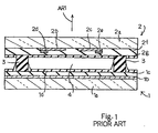
- Figure 1 illustrates the structure of a pixel incorporated in the prior art pulse memory driving type alternating current plasma display panel.
- the pixel comprises a back substrate structure 1 and a front substrate structure 2, and a partition wall 3 spaces the back substrate structure 1 from the front substrate 2.
- Discharging gas 4 such as helium, neon, xenon or gaseous mixture thereof fills the space between the back substrate structure 1 and the front substrate structure 2.
- the discharging gas generates ultra-violet light during discharging.
- the back substrate structure 1 includes a transparent glass plate 1a, and a data electrode 1b is formed on the transparent glass plate 1a.
- the data electrode 1b is covered with a dielectric layer 1c, and a phosphor layer 1d is laminated on the dielectric layer 1c.
- the ultra-violet tight is radiated onto the phosphor layer 1d, and the phosphor layer 1d converts the ultra-violet light to visible light.
- the visible tight is radiated as indicated by arrow AR1.
- the front substrate structure 2 includes a transparent glass plate 2a. and a scanning electrode 2b and a sustain electrode 2c are formed on the transparent glass plate 2a.
- the scanning electrode 2b and the sustain electrode 2c extend in the perpendicular direction to the data electrode 1b.
- Trace electrodes 2d/2e are laminated on the scanning electrode 2b and the sustain electrode 2c, respectively, and are expected to reduce the resistance against a scanning signal and a sustain signal.
- These electrodes 2b, 2c, 2d and 2e are covered with a dielectric layer 2f, and the dielectric layer 2f is overlain by a protective layer 2g.
- the protective layer 2g is formed of magnesium oxide, and prevents the dielectric layer 2f from the discharge.
- the prior art pixel shown in figure 1 produces a piece of image as follows. Firstly, initial potential larger than the discharging threshold is applied between the scanning electrode 2b and the data electrode 1b, and discharging take place therebetween. Positive charge and negative charge are attracted toward the dielectric layers 2f/1c over the scanning electrode 2b and the data electrode 1b, and are accumulated thereon as wall charges. The wali charges produce potential barriers, and gradually decrease the effective potential. For this reason, even if the initial potential is maintained between the scanning electrode 2b and the data electrode 1b, the prior art pixel stops the discharge.
- a sustain pulse is applied between the scanning electrode 2b and the sustain electrode 2c, and is identical in polarity with the wall potential.
- the wall potential is superposed on the sustain pulse. For this reason, even though the amplitude of the sustain pulse is low, the potential exceeds over the discharging threshold, and continues the discharging. Thus, while the sustain pulse is being applied between the scanning electrode 2b and the sustain electrode 2c, the sustain discharging is continued. This is the memory function.
- the erase pulse has wide pulse width and low amplitude or narrow width.
- Figure 2 illustrates the layout of pixels incorporated in the pulse memory driving type alternating current plasma display panel.
- the pixels 5 are identical in structure with the prior art pixel shown in figure 1, and form a display area 6.
- the pixels 5 are arranged in j rows and k columns, and a small box stands for each pixel 5 in figure 2.
- Scanning electrodes Sc1 to Scj and sustain electrodes Su1 to Suj extend in the direction of rows, and the scanning electrodes Sc1 to Scj are respectively paired with the sustain electrodes Su1 to Suj.
- the pairs of scanning/sustain electrodes Sc1/Su1 to Scj/Suj are respectively associated with the rows of pixels 5.
- data electrodes extend in the direction of columns, and are associated with the columns of pixels 5, respectively.
- Figure 3 illustrates the prior art method for controlling the alternating current plasma display panel shown in figure 2. and the prior art method is disclosed by Nakamura et al in "Drive for 40-in.-Diagonal Full-Color ac Plasma Display", Society for Information Display lnternational Symposium Digest of Technical Papers, volume XXVI, pages S07 to 810.
- Priming discharge period A, write-in period B and sustain discharge period C form each field, and a driving cycle or a frame has field 1 and field 2.
- a sustain electrode driving signal Wu is supplied to all the sustain electrodes Su1 to Suj, and scanning electrode4 driving signals Ws1, Ws2 ... Wsj are respectively supplied to the scanning electrodes Sc1 to Scj.
- a data electrode driving signal Wd is selectively supplied to the data electrodes D1 to Dk.
- the priming discharge pulse Pp is applied to all the sustain electrodes Su1 to Suj, and causes the priming discharge to take place in all the pixels 5.
- the priming discharge produces the wall charges.
- an erase pulse Ppe is concurrently supplied to the scanning electrodes Sc1 to Scj.
- the scanning pulse Pw is sequentially supplied to the scanning electrodes Ws1 to Wsj, and a data pulse Pd is selectively supplied to the data electrodes D1 to Dk associated with the pixels to emit the visible light in synchronism with the scanning pulse Pw. Then, write-in discharge takes place in the pixels 5 to emit the visible light, and the wall charge is produced for the pixels 5.
- the data pulse Pd is concurrently applied to all the data electrode D1 to Dk, and the photo-emitting current starts to flow at respective timings when both scanning and data pulses Pw/Pd take place between the scanning electrodes Sc1 to Scj and the data electrodes D1 to Dk.
- a sustain pulse Pc is supplied to the sustain electrodes Su1 to Suj, and, another sustain pulse Ps is supplied to the scanning electrodes Sc1 to Scj.
- the sustain pulse Ps is different in phase from the sustain pulse Pc at 180 degrees.
- the sustain pulses Pc/Ps maintains the luminance of the pixels 5 selected in the write-in period B.
- the plasma display panel is appropriate for a wide display area.
- the plasma display panel produces an image through gas discharge in the pixels, and requires a large amount of photo-emitting current for the gas discharge. If the potential difference is low due to large output impedance of driving circuits and large resistance of the electrodes Sc1-Scj and D1 to Dk, the potential range for the pulses is tight, and the illuminance is decreased.
- the pixels 5 require a large amount of current for the gas discharge.
- the output impedance of the drivers and the resistance of the scanning electrodes Sc1 to Scj strongly affect the amount of current, and the pulse height tends to be decreased. In this situation, the driver is expected to increase the pulse height of the data pulse Pd, or the designer is required to decrease the output impedance of the driver for the scanning electrodes Sc1 to Scj.
- the data electrodes are prolonged, and the parasitic capacitance cotrpled to each electrode is increased. Moreover, the pulses are driven at higher frequency. This results in heavy load to be driven by the driver and, accordingly, a large amount of electric power consumption.
- the plasma display panel requires strong drivers for a wide display area 6, and the strong drivers increases the production cost. The reduction of output impedance also results in expensive drivers, and the expensive drivers increases the production cost.
- the driver is incorporated in the prior art plasma display panel for the data electrodes D1 to Dk, and is expected to drive all the data electrodes D1 to Dk.
- the load of the driver is proportionally increased together with the resolution and the display area.
- Figure 4 illustrates relation between the minimum potential of the data pulse Pd required for the write-in discharge and the image data per each scanning electrode. If the pixels to be fired are equal to or less than 50 percent, the minimum potential is substantially constant. However, when the pixels to be fired exceed 50 percent, the minimum potential is increased as indicated by plots PL1.
- the driver lifts the potential level of the data electrodes D1 to Dk to or over the minimum potential at 100 percent. If the data electrodes D1 to Dk are lower than the minimum potential level, some pixels are misfired, and misfired pixels deteriorate the image produced on the display area 6. For this reason, the driver is expected to stably drive the data electrodes D1 to Dk, and the strong driver is expensive.
- Figure 5 illustrates another prior art surface discharge alternating current plasma display panel disclosed in Japanese Patent Publication of Unexamined Application No. 8-305319.
- Small circles stand for pixels 7, respectively.
- the pixels 7 are arranged in rows and columns, and form a display area 8.
- the rows of pixels 7 are respectively associated with scanning electrodes Sc1 to Scj and sustain electrodes Su1 to Suj, and the columns of pixels 7 are associated with data electrodes D1 to Dg and Dg+1 to D2g
- the data electrodes D1 to Dg and Dg+1 to D2g are divided into two data groups G1 and G2.
- Figure 6 illustrates the prior art method for controlling the alternating current plasma display panel shown in figure 5.
- Iw1 to lwj stand for discharge current flowing through the scanning electrodes Sc1 to Scj, respectively.
- a data pulse Pda is applied to the data electrodes D1 to Dg
- a data pulse Pdb is applied to the data electrodes Dg+1 to D2g.
- Time delay is introduced between the data pulse Pda and the data pulse Pdb, and is 400 nanosecond in the prior art alternating current plasma display panel. For this reason, the discharge current lw1 to lwj have two peaks, and the peak current is smaller than the peak current of the prior art alternating current plasma display panel shown in figure 2.
- the prior art method shown in figure 6 allows the manufacturer to decrease the peak current, and makes the potential drop due to the output impedance of the driver and the resistance of the electrodes.
- the data pulse Pda is equal in pulse width to the scanning pulse Pw. If the driver successively supplies the data pulse Pda to the data electrodes adjacent to each other, the driver does not recover the data pulse Pw to zero. The driver pulls down the data pulse Pda to a certain level, and raises the data pulse Pda from the certain level. For this reason, the power consumption is relatively small for the data pulse Pda.
- the data pulse Pdb is supplied to the data electrodes Dg+1 to D2g at intervals.
- the driver is expected to recover the data pulse Pdb to zero between the data pulses Pdb, and is expected to fully swing the data pulse Pdb. This results in a large amount of power consumption.
- the driver for the data pulse Pdb is expected to drive the load heavier than that of the driver for the data pulse Pda, and the driver for the data pulse Pdb tends to be heated higher than the other driver for the data pulse Pdb.
- the present invention proposes to change the order of data pulses.
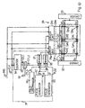
- FIG 7 illustrates a pulse memory driving type alternating current plasma display panel embodying the present invention
- the plasma display panel comprises a display area 21 for producing a picture, scanning electrodes Sc1 to Scj, sustain electrodes Su1 to Suj and data electrodes Da1 to Dam and Db1 to Dbn.
- the display area 21 is implemented by an array of pixels Ca11/Ca12 and Cb11/Cb12.
- the rows of pixels Ca11-Cam1-Cbl1-Cbn1/Ca12-Cam2-Cb12-Cbn2/ Ca13-Cam3-Cb13-Cbn3/.../ Ca1j-Camj-Cb1j-Cbnj are respectively associated with the scanning electrodes Sc1 to Scj, and are further associated with the sustain electrodes Su1 to Suj, respectively.
- the columns of pixels Ca11-Ca1j/ ../Cam1-Camj and Cb11-Cb1j/.. /Cbn1-Cbnj are respectively associated with the data electrodes Da1 to Dam and Db1 to Dbn.
- the structure of each pixel Ca11 to Cbnj is similar to the pixel 1, and no further description is incorporated hereinbelow for the sake of simplicity.
- the plasma display panel further comprises a driver 22 for sequentially driving the scanning electrodes Sc1 to Scj, a driver 23 for concurrently driving the sustain electrodes Su1 to Suj and a driver 24 for selectively driving the data electrodes Da1 to Dam and Db1 to Dbn.
- the driver 24 includes two driver units 24a and 24b, and the data electrodes Da1 to Dam and the data electrodes Db1 to Dbn are connected to the driver units 24a and 24b. respectively.
- the data electrodes Da1 to Dam and the data electrodes Db1 to Dbn are divided into two data electrode groups DA and DB.
- Figure 8 illustrates a method for controlling the plasma display panel according to the present invention.
- the drivers 22/23/24 produce a picture on the display area 21, and field 1 and field 2 form each driving cycle or a frame.
- Each field is divided into a priming discharge period A, a write-in discharge period B and a sustain discharge period C.
- the drivers 23 and 22 supply, a priming discharge pulse Pp and an erasing pulse Pe to the sustain electrodes Su1 to Suj and the scanning electrodes Sc1 to Scj in the priming discharge period A.
- the priming pulse Pp gives rise to priming discharge in the pixels Ca11 to Cbnj so as to accumulate wall charges, and the erasing pulse Pe erases the wall charge undesirable for the write-in discharge.
- the driver 22 sequentially supplies a scanning pulse Pw to the scanning electrodes Sc1 to Scj, and the driver units 24a/24b selectively supply data pulses Pd1/Pd2 to the data electrodes Da1 to Dam and Db1 to Dbn so as to produce the wall potential in selected pixels through write-in discharge.
- Time delay Td is introduced between the data pulse Pd1 and the data pulse Pd2.
- the driver 24a firstly raises the data pulse Pd1, and, thereafter, the driver 24b raises the data pulse Pd2.
- the driver unit 24b firstly raises the data pulse Pd2, and, thereafter, the driver 24a raises the data pulse Pd1.
- the plasma display panel proceeds to the sustain discharge period C.
- the driver 23 supplies a sustain pulse Pc to the sustain electrodes Su1 to Suj, and the driver 22 supplies a sustain pulse Ps to the scanning electrodes Sc1 to Scj.
- the sustain pulse Ps is different from the sustain pulse Pc at 180 degrees, and the sustain pulses Pc and Ps maintain the discharge in the selected pixels.
- the pixels Ca11 to Cbnj are selectively fired so as to produce a picture on the display area 21.
- the drivers 22/23/24 controls the sustain electrodes Su1-Suj, the scanning electrodes Sc1-Scj and the data electrodes Da1-Dam and Db1-Dbn as shown in figure 9. Description is focused on the photo-emitting current at the pixels Ca11, Ca12, Cb11 and Cb12.
- the photo-emitting current flows at the pixels Ca11, Ca12, Cb11 and Cb12 in the priming discharge period A of the field 1. While the scanning pulse Pw on the scanning electrode Sc1 is staying in the active low level on the scanning electrode Sc1, the data pulse Pd1 on the data electrode Dal rises at time a so that the write-in discharge takes place at the pixel Ca11, and the data pulse Pd2 on the data electrode Db1 rises at time b so that the write-in discharge takes place at the pixel Cb11. The timing b is delayed from the timing a by Td.
- the scanning pulse Pw on the scanning electrode Sc1 is recovered to the ground level, and the scanning pulse Pw on the next scanning electrode Sc2 goes down from the ground level.
- the driver unit 24a continuously supplies the data pulse Pd1 to the data line Da1, and the write-in discharge takes place in the pixel Ca12 at time a' .
- the data pulse Pd2 is recovered to the ground level, and rises at time b', again, so as to fire the pixel Cb12. In this way, the selected pixels are sequentially fired in the write-in discharge period B of the field 1.
- the sustain pulses Pc/Ps cause the selected pixels to continuously fire in the sustain discharge period C of the field 1.
- the duty factor is exchanged between the data pulse Pd1 and the data pulse Pd2.
- the photo-emitting current also flows at the pixels Ca11, Ca12, Cb11 and Cb12 in the priming discharge period A of the field 2. While the scanning pulse Pw on the scanning electrode Sc1 is staying in the active low level on the scanning electrode Sc1. the data pulse Pd2 on the data electrode Db1 rises at time c , so that the write-in discharge takes place at the pixel Cb11, and the data pulse Pd1 on the data electrode Da1 rises at time d so that the write-in discharge takes place at the pixel Ca11. The timing d is delayed from the timing by Td.
- the scanning pulse Pw on the scanning electrode Sc1 is recovered to the ground level, and the scanning pulse Pw on the next scanning electrode Sc2 goes down from the ground level.
- the driver unit 24b continuously supplies the data pulse Pd1 to the data line Db1, and the write-in discharge takes place in the pixel Cb12 at time c' .
- the data pulse Pd1 is recovered to the ground level, and rises at time d', again, so as to fire the pixel Ca12. In this way, the selected pixels are sequentially fired in the write-in discharge period B of the field 2.
- the sustain pulses Pc/Ps cause the selected pixels to continuously fire in the sustain discharge period C of the field 2.
- the time delay Td is introduced between the data pulse Pd1 and the data pulse Pd2. and the peak value of the photo-emitting current is decreased rather than the peak value of the photo-emitting current of the prior art plasma display panel.
- the duty factor is exchanged between the data pulse Pd1 and the data pulse Pd2 so as to equalize the load between the driver unit 24a and the driver unit 24b.
- FIG. 10 illustrates another pulse memory driving type alternating current plasma display panel embodying the present invention
- a controller 31 is incorporated in the plasma display panel.
- the other components are similar to those of the first embodiment, and are labeled with the same references designating corresponding components of the first embodiment without detailed description.
- the controller 31 includes two pulse generators 32 and 33.
- the pulse generator 32 generates a first pulse signal PLS1 and a second pulse signal PLS2, and the first pulse signal PLS1 and the second pulse signal PLS2 are different in duty factor from one another.
- the first pulse signal PLS1 has a pulse width equal to the scanning period, and the second pulse signal PLS2 is delayed from the first pulse signal PLS1.
- Data pulses Pd11 and Pd 12 are produced from the first pulse signal PLS1 and the second pulse signal PLS2 as will be described hereinlater.
- the controller 3 further includes a counter 34 and a comparator 33.
- a data clock signal CLK and an image data signal IMG are supplied to the counter 34, and determines the number of pixels to be fired for each scanning electrode Sc1-Scj.
- the counter 34 produces a control data signal CTL1 representative of the number of pixels to be fired, and supplies the control data signal CTL to the comparator 35.
- a reference signal RF is representative of the maximum number of pixels fired under a low write-in potential level, and is supplied to the comparator 35.
- the comparator 35 compares the number of pixels to be fired with the maximum number of pixels to see whether or not the pixels to be fired are greater than the maximum number.
- the comparator 35 produces a control data signal CTL2 representative of the comparison result.
- the controller 31 further includes a field discriminator 36 and selectors 37/38.
- the data pulse Pd11 is as wide in pulse width as the scanning period in every field 1, and is delayed from the data pulse Pd12 in every field 2.
- the data pulse Pd12 is delayed from the data pulse Pd11 in field 1, and is as wide in pulse width as the scanning period in every field 2.
- the field discriminator 36 determines a current field to be field 1 or field 2, and produces a control data signal CTL3 representative of the current field.
- the selectors 37/38 are connected to the driver units 24a/24b, respectively, and are responsive to the control data signals CTL2/CTL3 so as to selectively supply the first pulse signal PLS1 and the second pulse signal PLS2 to the driver units 24a/24b.
- the image data signal IMG, the data clock signal CLK and first/second pulse signals PLS1/PLS2 are supplied to the driver units 24a/24b, and the driver units 24a/24b produces the data pulses Pd11/Pd12 so as to selectively supply the data pulses Pd11/Pd12 to the associated data electrodes Da1-Dam and Db1-Dbn.
- the selectors 37/38 respectively supply the first pulse signal PLS1 and the second pulse signal PLS2 to the driver units 24a/24b in field 1, and the second pulse signal PLS2 and the first pulse signal PLS1 to the driver units 24a/24b in field 2.
- the selectors 37/38 supply the first pulse signal PLS1 to the driver units 24a/24b in every field.
- Figure 11 illustrates another method for controlling the plasma display panel according to the present invention.
- the priming discharge period A and the sustain discharge period C are similar to those of the first embodiment, and description is focused on the write-in discharge period B.
- the pixels indicated by black boxes in figure 7 are assumed to be fired.
- the number of pixels to be fired on the scanning electrode Sc1 is greater than the maximum number, and the number of pixels to be fired on the scanning electrode Sc2 is less than the maximum number.
- the scanning pulse Pw on the scanning electrode Sc1 goes down at time a, and the data pulse Pd11 on the data line Dal rises at the same timing. Then, the write-in discharge take, place at the pixel Ca11. The data pulse Pd12 on the data electrode Db1 rises at time b , and the pixel Cb11 is fired. Time delay Td is introduced between the data pulse Pd11 and the data pulse Pd12.
- the first pulse signal PLS1 is supplied to both driver units 24a/24b, and the driver units 24a/24b supplies the data pulses Pd11 and Pd12 as wide as the scanning pulse Pw to the data lines Da2/Db2 without fall to the ground level.
- the scanning pulse Pw on the scanning electrode Sc2 goes down at time e , and the pixels Ca12 and Cb12 are concurrently fired.
- the plasma display panel proceeds to field 2.
- the scanning pulse Pw on the scanning electrode Scl1 goes down at time c , and the data pulse Pd12 on the data line Dbl rises at the same timing.
- the write-in discharge takes place at the pixel Cb11.
- the data pulse Pd11 on the data electrode Da1 rises at time d , and the pixel Ca11 is fired.
- Time delay Td is also introduced between the data pulse Pd11 and the data pulse Pd12.
- the data pulse Pd12 rises earlier than the data pulse Pd11.
- the first pulse signal PLS1 is supplied to both driver units 24a/24b, and the driver units 24a/24b supplies the data pulses Pd11 and Pd12 as wide as the scanning pulse Pw to the data lines Da2/Db2 without fall to the ground level.
- the scanning pulse Pw on the scanning electrode Sc2 goes down at time f, and the pixels Ca12 and Cb12 are concurrently fired as similar to field 1.
- the driver units 24a/24b selectively supplies the first pulse signal PLS1 and the second pulse signal PLS2 to the driver units 24a/24b, because the pixels to be fired are greater than the maximum number.
- the first/second pulse signals PLS1/PLS2 are exchanged between the driver units 24a/24b, and the load is equalized between the driver units 24a and 24b.
- the data pulses Pd11/Pd12 are equal in width to the scanning pulse, and are not decayed to the ground level between the scanning electrodes Sc1 and Sc2. For this reason, the electric power consumption is reduced.
- the data lines or the frame may be divided into more than two groups.
- more than two data pulses are applied at different timings to the more than two groups, and duty factors are exchanged between the more than two data pulses.
- Each field may be divided into a plurality of sub-fields so as to grade the luminance into Y ⁇ 2 2 where Y is a constant and z is not less than zero and different between the sub-fields.
- the data pulses may be exchanged between the sub-fields.
- the odd electrodes and the even electrodes may form the data electrode groups DA and DB.
Landscapes
- Engineering & Computer Science (AREA)
- Physics & Mathematics (AREA)
- Power Engineering (AREA)
- Plasma & Fusion (AREA)
- Computer Hardware Design (AREA)
- General Physics & Mathematics (AREA)
- Theoretical Computer Science (AREA)
- Control Of Indicators Other Than Cathode Ray Tubes (AREA)
- Control Of Gas Discharge Display Tubes (AREA)
Description
- This invention relates to an alternating current plasma display panel and, more particularly, to a method for controlling a surface discharge alternating current plasma display panel.
- The plasma display panel has various attractive features such as a self-light emitting thin structure, a prompt response and a wide screen for producing a full-color large contrast image without flicker. These features are desirable for an interface between a computer and an operator.
- The plasma display panel is broken down into two categories. The first category is an alternating current plasma display panel, which has electrodes covered with dielectric material so as to indirectly discharge electric charges under application of alternating current. The second category is direct current plasma display panel, which has electrodes exposed to discharging space so as to produce direct discharge. The alternating current plasma display panel is further broken down into two sub-categories, i.e., a pulse memory driving type alternating current plasma display panel and a refresh type alternating current plasma display panel.
- The luminance of the alternating current plasma display panel is proportional to the number of discharges or the repetition of pulses applied to the electrodes. The refresh type alternating current plasma display panel decreases the luminescence inversely proportional to the display area, and, for this reason, is appropriate for a small image producing apparatus.
- Figure 1 illustrates the structure of a pixel incorporated in the prior art pulse memory driving type alternating current plasma display panel. The pixel comprises a
back substrate structure 1 and afront substrate structure 2, and apartition wall 3 spaces theback substrate structure 1 from thefront substrate 2. Discharginggas 4 such as helium, neon, xenon or gaseous mixture thereof fills the space between theback substrate structure 1 and thefront substrate structure 2. The discharging gas generates ultra-violet light during discharging. - The
back substrate structure 1 includes atransparent glass plate 1a, and adata electrode 1b is formed on thetransparent glass plate 1a. Thedata electrode 1b is covered with adielectric layer 1c, and a phosphor layer 1d is laminated on thedielectric layer 1c. The ultra-violet tight is radiated onto the phosphor layer 1d, and the phosphor layer 1d converts the ultra-violet light to visible light. The visible tight is radiated as indicated by arrow AR1. - The
front substrate structure 2 includes a transparent glass plate 2a. and ascanning electrode 2b and asustain electrode 2c are formed on thetransparent glass plate 2a. Thescanning electrode 2b and thesustain electrode 2c extend in the perpendicular direction to thedata electrode 1b. Trace electrodes 2d/2e are laminated on thescanning electrode 2b and thesustain electrode 2c, respectively, and are expected to reduce the resistance against a scanning signal and a sustain signal. Theseelectrodes dielectric layer 2f, and thedielectric layer 2f is overlain by aprotective layer 2g. Theprotective layer 2g is formed of magnesium oxide, and prevents thedielectric layer 2f from the discharge. - The prior art pixel shown in figure 1 produces a piece of image as follows. Firstly, initial potential larger than the discharging threshold is applied between the
scanning electrode 2b and thedata electrode 1b, and discharging take place therebetween. Positive charge and negative charge are attracted toward thedielectric layers 2f/1c over thescanning electrode 2b and thedata electrode 1b, and are accumulated thereon as wall charges. The wali charges produce potential barriers, and gradually decrease the effective potential. For this reason, even if the initial potential is maintained between thescanning electrode 2b and thedata electrode 1b, the prior art pixel stops the discharge. - Thereafter, a sustain pulse is applied between the
scanning electrode 2b and thesustain electrode 2c, and is identical in polarity with the wall potential. The wall potential is superposed on the sustain pulse. For this reason, even though the amplitude of the sustain pulse is low, the potential exceeds over the discharging threshold, and continues the discharging. Thus, while the sustain pulse is being applied between thescanning electrode 2b and thesustain electrode 2c, the sustain discharging is continued. This is the memory function. - When an erase pulse is applied between the
scanning pulse 2b and thesustain pulse 2c, the wall potential is canceled, and the pixel stops the sustain discharge. The erase pulse has wide pulse width and low amplitude or narrow width. - Figure 2 illustrates the layout of pixels incorporated in the pulse memory driving type alternating current plasma display panel. The
pixels 5 are identical in structure with the prior art pixel shown in figure 1, and form adisplay area 6. Thepixels 5 are arranged in j rows and k columns, and a small box stands for eachpixel 5 in figure 2. Scanning electrodes Sc1 to Scj and sustain electrodes Su1 to Suj extend in the direction of rows, and the scanning electrodes Sc1 to Scj are respectively paired with the sustain electrodes Su1 to Suj. The pairs of scanning/sustain electrodes Sc1/Su1 to Scj/Suj are respectively associated with the rows ofpixels 5. On the other hand, data electrodes extend in the direction of columns, and are associated with the columns ofpixels 5, respectively. - Figure 3 illustrates the prior art method for controlling the alternating current plasma display panel shown in figure 2. and the prior art method is disclosed by Nakamura et al in "Drive for 40-in.-Diagonal Full-Color ac Plasma Display", Society for Information Display lnternational Symposium Digest of Technical Papers, volume XXVI, pages S07 to 810. Priming discharge period A, write-in period B and sustain discharge period C form each field, and a driving cycle or a frame has
field 1 andfield 2. A sustain electrode driving signal Wu is supplied to all the sustain electrodes Su1 to Suj, and scanning electrode4 driving signals Ws1, Ws2 ... Wsj are respectively supplied to the scanning electrodes Sc1 to Scj. A data electrode driving signal Wd is selectively supplied to the data electrodes D1 to Dk. - Active particles and the wall charges are produced in the priming discharge period A so as to obtain stable write-in discharge characteristics. The priming discharge pulse Pp is applied to all the sustain electrodes Su1 to Suj, and causes the priming discharge to take place in all the
pixels 5. The priming discharge produces the wall charges. In order to erase the wall charge undesirable for the sustain discharge, an erase pulse Ppe is concurrently supplied to the scanning electrodes Sc1 to Scj. - In the write-in period B, the scanning pulse Pw is sequentially supplied to the scanning electrodes Ws1 to Wsj, and a data pulse Pd is selectively supplied to the data electrodes D1 to Dk associated with the pixels to emit the visible light in synchronism with the scanning pulse Pw. Then, write-in discharge takes place in the
pixels 5 to emit the visible light, and the wall charge is produced for thepixels 5. The data pulse Pd is concurrently applied to all the data electrode D1 to Dk, and the photo-emitting current starts to flow at respective timings when both scanning and data pulses Pw/Pd take place between the scanning electrodes Sc1 to Scj and the data electrodes D1 to Dk. - In the sustain discharge period C, a sustain pulse Pc is supplied to the sustain electrodes Su1 to Suj, and, another sustain pulse Ps is supplied to the scanning electrodes Sc1 to Scj. The sustain pulse Ps is different in phase from the sustain pulse Pc at 180 degrees. The sustain pulses Pc/Ps maintains the luminance of the
pixels 5 selected in the write-in period B. - As described hereinbefore, the plasma display panel is appropriate for a wide display area. The plasma display panel produces an image through gas discharge in the pixels, and requires a large amount of photo-emitting current for the gas discharge. If the potential difference is low due to large output impedance of driving circuits and large resistance of the electrodes Sc1-Scj and D1 to Dk, the potential range for the pulses is tight, and the illuminance is decreased. Especially, when a large number of
pixels 5 are selected from thedisplay area 6 in the write-in period B, thepixels 5 require a large amount of current for the gas discharge. However, the output impedance of the drivers and the resistance of the scanning electrodes Sc1 to Scj strongly affect the amount of current, and the pulse height tends to be decreased. In this situation, the driver is expected to increase the pulse height of the data pulse Pd, or the designer is required to decrease the output impedance of the driver for the scanning electrodes Sc1 to Scj. - When the
pixels 5 are increased for awide display area 6, the data electrodes are prolonged, and the parasitic capacitance cotrpled to each electrode is increased. Moreover, the pulses are driven at higher frequency. This results in heavy load to be driven by the driver and, accordingly, a large amount of electric power consumption. In short, the plasma display panel requires strong drivers for awide display area 6, and the strong drivers increases the production cost. The reduction of output impedance also results in expensive drivers, and the expensive drivers increases the production cost. - Though not shown in figure 2, the driver is incorporated in the prior art plasma display panel for the data electrodes D1 to Dk, and is expected to drive all the data electrodes D1 to Dk. The load of the driver is proportionally increased together with the resolution and the display area.
- Figure 4 illustrates relation between the minimum potential of the data pulse Pd required for the write-in discharge and the image data per each scanning electrode. If the pixels to be fired are equal to or less than 50 percent, the minimum potential is substantially constant. However, when the pixels to be fired exceed 50 percent, the minimum potential is increased as indicated by plots PL1. The driver lifts the potential level of the data electrodes D1 to Dk to or over the minimum potential at 100 percent. If the data electrodes D1 to Dk are lower than the minimum potential level, some pixels are misfired, and misfired pixels deteriorate the image produced on the
display area 6. For this reason, the driver is expected to stably drive the data electrodes D1 to Dk, and the strong driver is expensive. - Figure 5 illustrates another prior art surface discharge alternating current plasma display panel disclosed in Japanese Patent Publication of Unexamined Application No. 8-305319. Small circles stand for
pixels 7, respectively. Thepixels 7 are arranged in rows and columns, and form adisplay area 8. The rows ofpixels 7 are respectively associated with scanning electrodes Sc1 to Scj and sustain electrodes Su1 to Suj, and the columns ofpixels 7 are associated with data electrodes D1 to Dg and Dg+1 to D2g The data electrodes D1 to Dg and Dg+1 to D2g are divided into two data groups G1 and G2. - Figure 6 illustrates the prior art method for controlling the alternating current plasma display panel shown in figure 5. Iw1 to lwj stand for discharge current flowing through the scanning electrodes Sc1 to Scj, respectively. In the write-in period, a data pulse Pda is applied to the data electrodes D1 to Dg, and a data pulse Pdb is applied to the data electrodes Dg+1 to D2g. Time delay is introduced between the data pulse Pda and the data pulse Pdb, and is 400 nanosecond in the prior art alternating current plasma display panel. For this reason, the discharge current lw1 to lwj have two peaks, and the peak current is smaller than the peak current of the prior art alternating current plasma display panel shown in figure 2.
- The prior art method shown in figure 6 allows the manufacturer to decrease the peak current, and makes the potential drop due to the output impedance of the driver and the resistance of the electrodes. Moreover, the data pulse Pda is equal in pulse width to the scanning pulse Pw. If the driver successively supplies the data pulse Pda to the data electrodes adjacent to each other, the driver does not recover the data pulse Pw to zero. The driver pulls down the data pulse Pda to a certain level, and raises the data pulse Pda from the certain level. For this reason, the power consumption is relatively small for the data pulse Pda.
- On the other hand, the data pulse Pdb is supplied to the data electrodes Dg+1 to D2g at intervals. The driver is expected to recover the data pulse Pdb to zero between the data pulses Pdb, and is expected to fully swing the data pulse Pdb. This results in a large amount of power consumption.
- Thus, the driver for the data pulse Pdb is expected to drive the load heavier than that of the driver for the data pulse Pda, and the driver for the data pulse Pdb tends to be heated higher than the other driver for the data pulse Pdb.
- It is therefore an important object of the present invention to provide a method for controlling an alternating current plasma display panel which eliminates the unbalance from drivers for data electrodes without increase of peak current.
- To accomplish the object, the present invention proposes to change the order of data pulses.
- The invention is set forth in the attached
claim 1. - The features and advantages of the method for controlling an alternating current plasma display panel will be more clearly understood from the following description taken in conjunction with the accompanying drawings in which:
- Fig. 1 is a cross sectional view showing the structure of the prior art pixel;
- Fig. 2 is a plan view showing the layout of the pixels and the electrodes incorporated in the prior art pulse memory driving type alternating current plasma display panel,
- Fig. 3 is a timing chart showing the prior art method for controlling the alternating current plasma display panel;
- Fig. 4 is a graph showing the minimum potential of the data pulse in terms of the pixels to be fired along each scanning line;
- Fig. 5 is a plan view showing the layout of the pixels and the electrodes incorporated in the prior art pulse memory driving type alternating current plasma display panel,
- Fig. 6 is a timing chart showing the prior art method for controlling the alternating current plasma display panel;
- Fig. 7 is a schematic view showing a pulse memory driving type alternating current plasma display panel according to the present invention;
- Fig. 8 is a timing chart showing a method for controlling the pulse memory driving type alternating current plasma display panel according to the present invention;
- Fig. 9 is a timing chart showing a control sequence for selectively firing pixels;
- Fig. 10 is a schematic view showing another pulse memory driving type alternating current plasma display panel according to the present invention; and
- Fig. 11 is a timing chart showing a method for controlling the pulse memory driving type alternating current plasma display panel according to the present invention.
- Referring to figure 7 illustrates a pulse memory driving type alternating current plasma display panel embodying the present invention The plasma display panel comprises a
display area 21 for producing a picture, scanning electrodes Sc1 to Scj, sustain electrodes Su1 to Suj and data electrodes Da1 to Dam and Db1 to Dbn. Thedisplay area 21 is implemented by an array of pixels Ca11/Ca12 and Cb11/Cb12. The rows of pixels Ca11-Cam1-Cbl1-Cbn1/Ca12-Cam2-Cb12-Cbn2/ Ca13-Cam3-Cb13-Cbn3/.../ Ca1j-Camj-Cb1j-Cbnj are respectively associated with the scanning electrodes Sc1 to Scj, and are further associated with the sustain electrodes Su1 to Suj, respectively. On the other hand, the columns of pixels Ca11-Ca1j/ ../Cam1-Camj and Cb11-Cb1j/.. /Cbn1-Cbnj are respectively associated with the data electrodes Da1 to Dam and Db1 to Dbn. The structure of each pixel Ca11 to Cbnj is similar to thepixel 1, and no further description is incorporated hereinbelow for the sake of simplicity. - The plasma display panel further comprises a
driver 22 for sequentially driving the scanning electrodes Sc1 to Scj, adriver 23 for concurrently driving the sustain electrodes Su1 to Suj and adriver 24 for selectively driving the data electrodes Da1 to Dam and Db1 to Dbn. Thedriver 24 includes twodriver units driver units - Figure 8 illustrates a method for controlling the plasma display panel according to the present invention. The
drivers 22/23/24 produce a picture on thedisplay area 21, andfield 1 andfield 2 form each driving cycle or a frame. Each field is divided into a priming discharge period A, a write-in discharge period B and a sustain discharge period C. - The
drivers - Subsequently, the
driver 22 sequentially supplies a scanning pulse Pw to the scanning electrodes Sc1 to Scj, and thedriver units 24a/24b selectively supply data pulses Pd1/Pd2 to the data electrodes Da1 to Dam and Db1 to Dbn so as to produce the wall potential in selected pixels through write-in discharge. Time delay Td is introduced between the data pulse Pd1 and the data pulse Pd2. Infield 1, thedriver 24a firstly raises the data pulse Pd1, and, thereafter, thedriver 24b raises the data pulse Pd2. However, when the plasma display panel proceeds tofield 2, thedriver unit 24b firstly raises the data pulse Pd2, and, thereafter, thedriver 24a raises the data pulse Pd1. - The plasma display panel proceeds to the sustain discharge period C. The
driver 23 supplies a sustain pulse Pc to the sustain electrodes Su1 to Suj, and thedriver 22 supplies a sustain pulse Ps to the scanning electrodes Sc1 to Scj. The sustain pulse Ps is different from the sustain pulse Pc at 180 degrees, and the sustain pulses Pc and Ps maintain the discharge in the selected pixels. Thus, the pixels Ca11 to Cbnj are selectively fired so as to produce a picture on thedisplay area 21. - In order to fire the pixels represented by black boxes in figure 7, the
drivers 22/23/24 controls the sustain electrodes Su1-Suj, the scanning electrodes Sc1-Scj and the data electrodes Da1-Dam and Db1-Dbn as shown in figure 9. Description is focused on the photo-emitting current at the pixels Ca11, Ca12, Cb11 and Cb12. - The photo-emitting current flows at the pixels Ca11, Ca12, Cb11 and Cb12 in the priming discharge period A of the
field 1. While the scanning pulse Pw on the scanning electrode Sc1 is staying in the active low level on the scanning electrode Sc1, the data pulse Pd1 on the data electrode Dal rises at time a so that the write-in discharge takes place at the pixel Ca11, and the data pulse Pd2 on the data electrode Db1 rises at time b so that the write-in discharge takes place at the pixel Cb11. The timing b is delayed from the timing a by Td. - The scanning pulse Pw on the scanning electrode Sc1 is recovered to the ground level, and the scanning pulse Pw on the next scanning electrode Sc2 goes down from the ground level. The
driver unit 24a continuously supplies the data pulse Pd1 to the data line Da1, and the write-in discharge takes place in the pixel Ca12 at time a'. The data pulse Pd2 is recovered to the ground level, and rises at time b', again, so as to fire the pixel Cb12. In this way, the selected pixels are sequentially fired in the write-in discharge period B of thefield 1. The sustain pulses Pc/Ps cause the selected pixels to continuously fire in the sustain discharge period C of thefield 1. - The duty factor is exchanged between the data pulse Pd1 and the data pulse Pd2. The photo-emitting current also flows at the pixels Ca11, Ca12, Cb11 and Cb12 in the priming discharge period A of the
field 2. While the scanning pulse Pw on the scanning electrode Sc1 is staying in the active low level on the scanning electrode Sc1. the data pulse Pd2 on the data electrode Db1 rises at time c, so that the write-in discharge takes place at the pixel Cb11, and the data pulse Pd1 on the data electrode Da1 rises at time d so that the write-in discharge takes place at the pixel Ca11. The timing d is delayed from the timing by Td. - The scanning pulse Pw on the scanning electrode Sc1 is recovered to the ground level, and the scanning pulse Pw on the next scanning electrode Sc2 goes down from the ground level. The
driver unit 24b continuously supplies the data pulse Pd1 to the data line Db1, and the write-in discharge takes place in the pixel Cb12 at time c'. The data pulse Pd1 is recovered to the ground level, and rises at time d', again, so as to fire the pixel Ca12. In this way, the selected pixels are sequentially fired in the write-in discharge period B of thefield 2. The sustain pulses Pc/Ps cause the selected pixels to continuously fire in the sustain discharge period C of thefield 2. - As will be appreciated from the foregoing description, the time delay Td is introduced between the data pulse Pd1 and the data pulse Pd2. and the peak value of the photo-emitting current is decreased rather than the peak value of the photo-emitting current of the prior art plasma display panel. Moreover, the duty factor is exchanged between the data pulse Pd1 and the data pulse Pd2 so as to equalize the load between the
driver unit 24a and thedriver unit 24b. - Figure 10 illustrates another pulse memory driving type alternating current plasma display panel embodying the present invention In this instance, a
controller 31 is incorporated in the plasma display panel. The other components are similar to those of the first embodiment, and are labeled with the same references designating corresponding components of the first embodiment without detailed description. - The
controller 31 includes twopulse generators pulse generator 32 generates a first pulse signal PLS1 and a second pulse signal PLS2, and the first pulse signal PLS1 and the second pulse signal PLS2 are different in duty factor from one another. The first pulse signal PLS1 has a pulse width equal to the scanning period, and the second pulse signal PLS2 is delayed from the first pulse signal PLS1. Data pulses Pd11 and Pd 12 are produced from the first pulse signal PLS1 and the second pulse signal PLS2 as will be described hereinlater. - The
controller 3 further includes acounter 34 and acomparator 33. A data clock signal CLK and an image data signal IMG are supplied to thecounter 34, and determines the number of pixels to be fired for each scanning electrode Sc1-Scj. Thecounter 34 produces a control data signal CTL1 representative of the number of pixels to be fired, and supplies the control data signal CTL to thecomparator 35. A reference signal RF is representative of the maximum number of pixels fired under a low write-in potential level, and is supplied to thecomparator 35. Thecomparator 35 compares the number of pixels to be fired with the maximum number of pixels to see whether or not the pixels to be fired are greater than the maximum number. Thecomparator 35 produces a control data signal CTL2 representative of the comparison result. - The
controller 31 further includes afield discriminator 36 andselectors 37/38. In this instance, the data pulse Pd11 is as wide in pulse width as the scanning period in everyfield 1, and is delayed from the data pulse Pd12 in everyfield 2. On the other hand, the data pulse Pd12 is delayed from the data pulse Pd11 infield 1, and is as wide in pulse width as the scanning period in everyfield 2. Thefield discriminator 36 determines a current field to befield 1 orfield 2, and produces a control data signal CTL3 representative of the current field. Theselectors 37/38 are connected to thedriver units 24a/24b, respectively, and are responsive to the control data signals CTL2/CTL3 so as to selectively supply the first pulse signal PLS1 and the second pulse signal PLS2 to thedriver units 24a/24b. - The image data signal IMG, the data clock signal CLK and first/second pulse signals PLS1/PLS2 are supplied to the
driver units 24a/24b, and thedriver units 24a/24b produces the data pulses Pd11/Pd12 so as to selectively supply the data pulses Pd11/Pd12 to the associated data electrodes Da1-Dam and Db1-Dbn. - If the number of pixels to be fired is greater than the maximum number, the
selectors 37/38 respectively supply the first pulse signal PLS1 and the second pulse signal PLS2 to thedriver units 24a/24b infield 1, and the second pulse signal PLS2 and the first pulse signal PLS1 to thedriver units 24a/24b infield 2. However, when the number of pixels to be fired is equal to or less than the maximum number, theselectors 37/38 supply the first pulse signal PLS1 to thedriver units 24a/24b in every field. - Figure 11 illustrates another method for controlling the plasma display panel according to the present invention. The priming discharge period A and the sustain discharge period C are similar to those of the first embodiment, and description is focused on the write-in discharge period B. The pixels indicated by black boxes in figure 7 are assumed to be fired. The number of pixels to be fired on the scanning electrode Sc1 is greater than the maximum number, and the number of pixels to be fired on the scanning electrode Sc2 is less than the maximum number.
- The scanning pulse Pw on the scanning electrode Sc1 goes down at time a, and the data pulse Pd11 on the data line Dal rises at the same timing. Then, the write-in discharge take, place at the pixel Ca11. The data pulse Pd12 on the data electrode Db1 rises at time b, and the pixel Cb11 is fired. Time delay Td is introduced between the data pulse Pd11 and the data pulse Pd12.
- The first pulse signal PLS1 is supplied to both
driver units 24a/24b, and thedriver units 24a/24b supplies the data pulses Pd11 and Pd12 as wide as the scanning pulse Pw to the data lines Da2/Db2 without fall to the ground level. The scanning pulse Pw on the scanning electrode Sc2 goes down at time e, and the pixels Ca12 and Cb12 are concurrently fired. - The plasma display panel proceeds to
field 2. The scanning pulse Pw on the scanning electrode Scl1 goes down at time c, and the data pulse Pd12 on the data line Dbl rises at the same timing. Then, the write-in discharge takes place at the pixel Cb11. The data pulse Pd11 on the data electrode Da1 rises at time d, and the pixel Ca11 is fired. Time delay Td is also introduced between the data pulse Pd11 and the data pulse Pd12. However, the data pulse Pd12 rises earlier than the data pulse Pd11. - The first pulse signal PLS1 is supplied to both
driver units 24a/24b, and thedriver units 24a/24b supplies the data pulses Pd11 and Pd12 as wide as the scanning pulse Pw to the data lines Da2/Db2 without fall to the ground level. The scanning pulse Pw on the scanning electrode Sc2 goes down at time f, and the pixels Ca12 and Cb12 are concurrently fired as similar tofield 1. - As will be understood from the foregoing description, the
driver units 24a/24b selectively supplies the first pulse signal PLS1 and the second pulse signal PLS2 to thedriver units 24a/24b, because the pixels to be fired are greater than the maximum number. However, the first/second pulse signals PLS1/PLS2 are exchanged between thedriver units 24a/24b, and the load is equalized between thedriver units - Moreover, when the pixels to be fired on the scanning electrode Sc2 is less than the maximum number, the data pulses Pd11/Pd12 are equal in width to the scanning pulse, and are not decayed to the ground level between the scanning electrodes Sc1 and Sc2. For this reason, the electric power consumption is reduced.
- Although particular embodiments of the present invention have been shown and described, it will be obvious to those skilled in the art that various changes and modifications may be made without departing from the scope of the present invention as defined in the appended claims.
- For example, the data lines or the frame may be divided into more than two groups. In this instance, more than two data pulses are applied at different timings to the more than two groups, and duty factors are exchanged between the more than two data pulses.
- Each field may be divided into a plurality of sub-fields so as to grade the luminance into Y × 22 where Y is a constant and z is not less than zero and different between the sub-fields. The data pulses may be exchanged between the sub-fields.
- The odd electrodes and the even electrodes may form the data electrode groups DA and DB.
Claims (6)
- A method for controlling a plasma display panel having a plurality of scanning electrodes (Sc1 to Scj), a plurality of sustain electrodes (Su1 to Suj) respectively paired with said plurality of scanning electrodes for forming a plurality of electrode pairs, a plurality of data electrodes (Da1-Dam/Db1-Dbn) divided into a plurality of data electrode groups (DA/DB) and a plurality of pixels (Ca11-Cbnj) selectively associated with said plurality of electrode pairs and said plurality of data electrodes and selectively fired for forming an image, comprising the steps of:a) supplying a scanning pulse (Pw) sequentially to said scanning electrodes and a plurality of data pulses (Pd1/Pd2; Pd11/Pd12) different in duty factor and delayed from one another selectively to said plurality of data electrodes of said plurality of data electrode groups in a first phase (B) of a first field for selectively generating a write-in discharge in said plurality of pixels;b) supplying a first sustain pulse (Ps) and a second sustain pulse (Pc) dif ferent in phase from said first sustain pulse to said plurality of scanning electrodes and said plurality of sustain electrodes in a second phase (C) of said first field for keeping the pixels, in which the write-in discharge has been generated, fired;c) supplying said scanning pulse sequentially to said scanning electrodes and said plurality of data pulses of said first field selectively to said plurality of data electrodes of said plurality of data electrode groups in said first phase (B) of a second field for selectively generating said write-in discharge in said plurality of pixels; andd) supplying said first sustain pulse and said second sustain pulse to said plurality of scanning electrodes and said plurality of sustain electrodes in said second phase (C) of said second field for keeping the pixels, in which the write-in discharge has been generated, fired.characterized in that
for each data electrode the data pulse applied in said step c) is changed in duty factor from the data pulse applied to that data electrode said step a). - The method as set forth in claim 1, in which one of said Plurality of data pulses (Pd1; Pd11) in said step a) and another of said plurality of data pulses (Pd2; Pd12) in said step c) are equal in pulse width to said scanning pulse, and said another of said plurality of data pulses (Pd2; Pd12) in said step a) and said one of said plurality of data pulses (Pd1; Pd11) in said step c) are smaller in pulse width than said one of said plurality of data pulses in said step a) and said another of said plurality of data pulses in said step c) and delayed therefrom.
- The method as set forth in claim 1, further comprising the step of supplying a priming discharge pulse (Pw) and an erasing pulse (Pe) to said plurality of sustain electrodes and said plurality of scanning electrodes so as to produce, a wall potential before said step a) and between said step b) and said step c).
- The method as set forth in claim 3, in which one of said plurality of data pulses (Pd1; Pd11) in said step a) and another of said plurality of data pulses (Pd2; Pd12) in said step c) are equal in pulse width to said scanning pulse, and said another of said plurality of data pulses (Pd2; Pd13) in said step a) and said one of said plurality of data pulses (Pd1; Pd11) in said step c) are smaller in pulse width than said one of said plurality of data pulses in said step a) and said another of said plurality of data pulses in said step c) and delayed therefrom.
- The method as set forth in claim 1, further comprising the step of determining the number of pixels (Ca11/Ca21/Cam-11/Cam1/Cb11/Cb21/Cbn-11/Cbn1; Ca12/Cb12) to be fired on each scanning electrode whether to be greater than a predetermined number or not before step a), and said predetermined number is indicative of the maximum number of pixels fired under a low potential level of a data pulse.
- The method as set forth in claim 5. in which said plurality of data electrodes are supplied with a data pulse (Pd11/Pd12) equal in width to said scanning pulse (Pw) instead of said plurality of data pulses in said steps a) and c) when said number of pixels to be fired is equal to or less than said predetermined number.
Applications Claiming Priority (2)
| Application Number | Priority Date | Filing Date | Title |
|---|---|---|---|
| JP9003108A JP2950270B2 (en) | 1997-01-10 | 1997-01-10 | Driving method of AC discharge memory type plasma display panel |
| JP3108/97 | 1997-01-10 |
Publications (2)
| Publication Number | Publication Date |
|---|---|
| EP0853306A1 EP0853306A1 (en) | 1998-07-15 |
| EP0853306B1 true EP0853306B1 (en) | 2006-04-05 |
Family
ID=11548163
Family Applications (1)
| Application Number | Title | Priority Date | Filing Date |
|---|---|---|---|
| EP98100080A Expired - Lifetime EP0853306B1 (en) | 1997-01-10 | 1998-01-05 | Method of reducing peak current in a plasma display panel |
Country Status (6)
| Country | Link |
|---|---|
| US (1) | US5990630A (en) |
| EP (1) | EP0853306B1 (en) |
| JP (1) | JP2950270B2 (en) |
| KR (1) | KR100275982B1 (en) |
| DE (1) | DE69834061T2 (en) |
| TW (1) | TW368644B (en) |
Cited By (2)
| Publication number | Priority date | Publication date | Assignee | Title |
|---|---|---|---|---|
| US7619588B2 (en) | 2004-11-19 | 2009-11-17 | Lg Electronics Inc. | Plasma display device and method for driving the same |
| US7649508B2 (en) | 2004-12-01 | 2010-01-19 | Lg Electronics Inc. | Plasma display apparatus and driving method thereof |
Families Citing this family (32)
| Publication number | Priority date | Publication date | Assignee | Title |
|---|---|---|---|---|
| JP3710592B2 (en) * | 1997-04-24 | 2005-10-26 | 三菱電機株式会社 | Driving method of plasma display |
| US6340866B1 (en) * | 1998-02-05 | 2002-01-22 | Lg Electronics Inc. | Plasma display panel and driving method thereof |
| WO2000000954A1 (en) * | 1998-06-30 | 2000-01-06 | Daewoo Electronics Co., Ltd. | Circuit for driving address electrodes of a plasma display panel system |
| US6271810B1 (en) * | 1998-07-29 | 2001-08-07 | Lg Electronics Inc. | Plasma display panel using radio frequency and method and apparatus for driving the same |
| JP3606429B2 (en) * | 1999-02-19 | 2005-01-05 | パイオニア株式会社 | Driving method of plasma display panel |
| US6501447B1 (en) * | 1999-03-16 | 2002-12-31 | Lg Electronics Inc. | Plasma display panel employing radio frequency and method of driving the same |
| US6320326B1 (en) * | 1999-04-08 | 2001-11-20 | Matsushita Electric Industrial Co., Ltd. | AC plasma display apparatus |
| KR100364696B1 (en) | 1999-10-28 | 2003-01-24 | 엘지전자 주식회사 | Method for driving plasma display panel and structure of the plasma display panel |
| JP3570496B2 (en) * | 1999-12-22 | 2004-09-29 | 日本電気株式会社 | Driving method of plasma display panel |
| JP2001272948A (en) | 2000-03-23 | 2001-10-05 | Nec Corp | Driving method of plasma display panel and plasma display device |
| CN1447960A (en) * | 2000-05-30 | 2003-10-08 | 皇家菲利浦电子有限公司 | Display panel having sustain electrodes and sustain circuit |
| US6624588B2 (en) * | 2001-06-22 | 2003-09-23 | Pioneer Corporation | Method of driving plasma display panel |
| KR20030097342A (en) * | 2002-06-20 | 2003-12-31 | 엘지전자 주식회사 | Method and apparatus for driving driving plasma display panel |
| KR100471980B1 (en) * | 2002-06-28 | 2005-03-10 | 삼성에스디아이 주식회사 | Plasma display panel having barrier and manufacturing method of the barrier |
| US9153168B2 (en) * | 2002-07-09 | 2015-10-06 | Semiconductor Energy Laboratory Co., Ltd. | Method for deciding duty factor in driving light-emitting device and driving method using the duty factor |
| CN100429687C (en) * | 2002-11-29 | 2008-10-29 | 松下电器产业株式会社 | Plasma display panel display device and driving method thereof |
| FR2857144A1 (en) * | 2003-07-03 | 2005-01-07 | Thomson Plasma | METHOD FOR CONTROLLING A PLASMA PANEL HAVING MATRIX STRIPPING ECHELONNE |
| JP2005338421A (en) * | 2004-05-27 | 2005-12-08 | Renesas Technology Corp | Liquid crystal display driving device and liquid crystal display system |
| KR100542239B1 (en) | 2004-08-03 | 2006-01-10 | 삼성에스디아이 주식회사 | Plasma display device and driving method thereof |
| KR100820632B1 (en) | 2004-08-27 | 2008-04-10 | 엘지전자 주식회사 | Plasma Display Panel Driving Method |
| KR100774909B1 (en) * | 2004-11-16 | 2007-11-09 | 엘지전자 주식회사 | Driving Method of Plasma Display Panel |
| KR100774908B1 (en) | 2004-11-16 | 2007-11-09 | 엘지전자 주식회사 | Driving Method of Plasma Display Panel |
| KR100774875B1 (en) * | 2004-11-16 | 2007-11-08 | 엘지전자 주식회사 | Driving Method of Plasma Display Panel |
| KR100701947B1 (en) * | 2005-01-13 | 2007-03-30 | 엘지전자 주식회사 | Plasma display panel |
| JP2006251624A (en) | 2005-03-14 | 2006-09-21 | Matsushita Electric Ind Co Ltd | Plasma display device |
| JP4977960B2 (en) * | 2005-04-11 | 2012-07-18 | パナソニック株式会社 | Plasma display device |
| KR100829249B1 (en) * | 2005-09-26 | 2008-05-14 | 엘지전자 주식회사 | Plasma display device and driving method thereof |
| KR100829019B1 (en) * | 2005-11-07 | 2008-05-14 | 엘지전자 주식회사 | Plasma display device and driving method thereof |
| KR100793101B1 (en) | 2006-01-04 | 2008-01-10 | 엘지전자 주식회사 | Plasma display device |
| KR20070108675A (en) * | 2006-05-08 | 2007-11-13 | 엘지전자 주식회사 | Plasma display panel |
| KR100793576B1 (en) | 2007-03-08 | 2008-01-14 | 삼성에스디아이 주식회사 | Driving Method of Plasma Display Panel |
| KR20090078532A (en) * | 2008-01-15 | 2009-07-20 | 삼성에스디아이 주식회사 | Plasma display device and driving method thereof |
Family Cites Families (13)
| Publication number | Priority date | Publication date | Assignee | Title |
|---|---|---|---|---|
| US4006298A (en) * | 1975-05-20 | 1977-02-01 | Gte Laboratories Incorporated | Bistable matrix television display system |
| JP2642956B2 (en) * | 1988-07-20 | 1997-08-20 | 富士通株式会社 | Plasma display panel driving method and circuit thereof |
| JP2687684B2 (en) * | 1990-06-08 | 1997-12-08 | 日本電気株式会社 | Driving method of plasma display panel |
| JP3088494B2 (en) * | 1991-07-26 | 2000-09-18 | 富士通株式会社 | Display device driving method and device |
| JPH064039A (en) * | 1992-06-19 | 1994-01-14 | Fujitsu Ltd | AC type plasma display panel and its driving circuit |
| JP3276406B2 (en) * | 1992-07-24 | 2002-04-22 | 富士通株式会社 | Driving method of plasma display |
| JPH0764508A (en) * | 1993-08-30 | 1995-03-10 | Fujitsu General Ltd | Display panel driving method and device thereof |
| US5684499A (en) * | 1993-11-29 | 1997-11-04 | Nec Corporation | Method of driving plasma display panel having improved operational margin |
| JPH07248744A (en) * | 1994-03-11 | 1995-09-26 | Fujitsu General Ltd | Driving method for plasma display |
| JPH07319424A (en) * | 1994-05-26 | 1995-12-08 | Matsushita Electron Corp | Driving method for gas discharge display device |
| JP2885127B2 (en) * | 1995-04-10 | 1999-04-19 | 日本電気株式会社 | Drive circuit for plasma display panel |
| JP2953342B2 (en) * | 1995-04-28 | 1999-09-27 | 日本電気株式会社 | Driving method of plasma display panel |
| JP3364066B2 (en) * | 1995-10-02 | 2003-01-08 | 富士通株式会社 | AC-type plasma display device and its driving circuit |
-
1997
- 1997-01-10 JP JP9003108A patent/JP2950270B2/en not_active Expired - Fee Related
- 1997-12-27 TW TW086119853A patent/TW368644B/en not_active IP Right Cessation
-
1998
- 1998-01-05 EP EP98100080A patent/EP0853306B1/en not_active Expired - Lifetime
- 1998-01-05 DE DE69834061T patent/DE69834061T2/en not_active Expired - Fee Related
- 1998-01-06 US US09/003,162 patent/US5990630A/en not_active Expired - Lifetime
- 1998-01-09 KR KR1019980000400A patent/KR100275982B1/en not_active Expired - Fee Related
Cited By (2)
| Publication number | Priority date | Publication date | Assignee | Title |
|---|---|---|---|---|
| US7619588B2 (en) | 2004-11-19 | 2009-11-17 | Lg Electronics Inc. | Plasma display device and method for driving the same |
| US7649508B2 (en) | 2004-12-01 | 2010-01-19 | Lg Electronics Inc. | Plasma display apparatus and driving method thereof |
Also Published As
| Publication number | Publication date |
|---|---|
| TW368644B (en) | 1999-09-01 |
| KR19980070436A (en) | 1998-10-26 |
| DE69834061D1 (en) | 2006-05-18 |
| DE69834061T2 (en) | 2007-03-08 |
| JPH10198304A (en) | 1998-07-31 |
| EP0853306A1 (en) | 1998-07-15 |
| KR100275982B1 (en) | 2000-12-15 |
| US5990630A (en) | 1999-11-23 |
| JP2950270B2 (en) | 1999-09-20 |
Similar Documents
| Publication | Publication Date | Title |
|---|---|---|
| US5990630A (en) | Method for controlling surface discharge alternating current plasma display panel with drivers periodically changing duty factor of data pulses | |
| USRE44757E1 (en) | Method for driving a gas-discharge panel | |
| US6970147B2 (en) | Drive apparatus for a plasma display panel and a drive method thereof | |
| US6295040B1 (en) | AC-type plasma display panel and its driving method | |
| EP0945844A2 (en) | Display and method of driving the display | |
| US20010024179A1 (en) | Plasma display with reduced power consumption | |
| JP2001228821A (en) | Plasma display device and driving method thereof | |
| WO2004055771A1 (en) | Plasma display panel drive method | |
| JP2001255849A (en) | Energy recovery device and method for PDP, and high-speed addressing method using the same | |
| US6281635B1 (en) | Separate voltage driving method and apparatus for plasma display panel | |
| US6833823B2 (en) | Method and device for driving AC type PDP | |
| EP1426916A2 (en) | Driver circuit for a plasma display panel | |
| US7098603B2 (en) | Method and apparatus for driving plasma display panel | |
| JP2004206093A (en) | Driving method of plasma display panel | |
| JP4240163B2 (en) | Driving method of plasma display panel | |
| JPH10222119A (en) | Driving method of plasma display panel | |
| US6281633B1 (en) | Plasma display panel driving apparatus | |
| KR100605763B1 (en) | Plasma Display Panel Driving Apparatus And Method | |
| US7439942B2 (en) | Plasma display panel driving apparatus | |
| JP2004093888A (en) | Method for driving plasma display panel | |
| KR100313116B1 (en) | Method for driving plasma display panel | |
| JP2006146215A (en) | Plasma display device and driving method thereof | |
| CN101206828A (en) | Device and method for driving a display | |
| KR20020096397A (en) | Driving Method for Scanning of Plasma Display Panel and Apparatus Thereof | |
| KR100528931B1 (en) | Discharge display apparatus wherein reset function is improved |
Legal Events
| Date | Code | Title | Description |
|---|---|---|---|
| PUAI | Public reference made under article 153(3) epc to a published international application that has entered the european phase |
Free format text: ORIGINAL CODE: 0009012 |
|
| 17P | Request for examination filed |
Effective date: 19980417 |
|
| AK | Designated contracting states |
Kind code of ref document: A1 Designated state(s): DE FR |
|
| AX | Request for extension of the european patent |
Free format text: AL;LT;LV;MK;RO;SI |
|
| AKX | Designation fees paid |
Free format text: DE FR |
|
| RBV | Designated contracting states (corrected) |
Designated state(s): DE FR |
|
| RAP1 | Party data changed (applicant data changed or rights of an application transferred) |
Owner name: NEC PLASMA DISPLAY CORPORATION |
|
| RAP1 | Party data changed (applicant data changed or rights of an application transferred) |
Owner name: PIONEER PLASMA DISPLAY CORPORATION |
|
| GRAP | Despatch of communication of intention to grant a patent |
Free format text: ORIGINAL CODE: EPIDOSNIGR1 |
|
| RAP1 | Party data changed (applicant data changed or rights of an application transferred) |
Owner name: PIONEER CORPORATION |
|
| GRAS | Grant fee paid |
Free format text: ORIGINAL CODE: EPIDOSNIGR3 |
|
| GRAA | (expected) grant |
Free format text: ORIGINAL CODE: 0009210 |
|
| AK | Designated contracting states |
Kind code of ref document: B1 Designated state(s): DE FR |
|
| REF | Corresponds to: |
Ref document number: 69834061 Country of ref document: DE Date of ref document: 20060518 Kind code of ref document: P |
|
| ET | Fr: translation filed | ||
| PLBE | No opposition filed within time limit |
Free format text: ORIGINAL CODE: 0009261 |
|
| STAA | Information on the status of an ep patent application or granted ep patent |
Free format text: STATUS: NO OPPOSITION FILED WITHIN TIME LIMIT |
|
| PGFP | Annual fee paid to national office [announced via postgrant information from national office to epo] |
Ref country code: DE Payment date: 20070329 Year of fee payment: 10 |
|
| 26N | No opposition filed |
Effective date: 20070108 |
|
| PGFP | Annual fee paid to national office [announced via postgrant information from national office to epo] |
Ref country code: FR Payment date: 20070118 Year of fee payment: 10 |
|
| PG25 | Lapsed in a contracting state [announced via postgrant information from national office to epo] |
Ref country code: DE Free format text: LAPSE BECAUSE OF NON-PAYMENT OF DUE FEES Effective date: 20080801 |
|
| REG | Reference to a national code |
Ref country code: FR Ref legal event code: ST Effective date: 20081029 |
|
| PG25 | Lapsed in a contracting state [announced via postgrant information from national office to epo] |
Ref country code: FR Free format text: LAPSE BECAUSE OF NON-PAYMENT OF DUE FEES Effective date: 20080131 |