EP0849663A2 - Conditional sum adder using pass-transistor logic - Google Patents
Conditional sum adder using pass-transistor logic Download PDFInfo
- Publication number
- EP0849663A2 EP0849663A2 EP97310722A EP97310722A EP0849663A2 EP 0849663 A2 EP0849663 A2 EP 0849663A2 EP 97310722 A EP97310722 A EP 97310722A EP 97310722 A EP97310722 A EP 97310722A EP 0849663 A2 EP0849663 A2 EP 0849663A2
- Authority
- EP
- European Patent Office
- Prior art keywords
- signal
- bit
- carry
- sum
- signals
- Prior art date
- Legal status (The legal status is an assumption and is not a legal conclusion. Google has not performed a legal analysis and makes no representation as to the accuracy of the status listed.)
- Granted
Links
Images


Classifications
-
- H—ELECTRICITY
- H03—ELECTRONIC CIRCUITRY
- H03K—PULSE TECHNIQUE
- H03K19/00—Logic circuits, i.e. having at least two inputs acting on one output; Inverting circuits
-
- G—PHYSICS
- G06—COMPUTING; CALCULATING OR COUNTING
- G06F—ELECTRIC DIGITAL DATA PROCESSING
- G06F7/00—Methods or arrangements for processing data by operating upon the order or content of the data handled
- G06F7/38—Methods or arrangements for performing computations using exclusively denominational number representation, e.g. using binary, ternary, decimal representation
- G06F7/48—Methods or arrangements for performing computations using exclusively denominational number representation, e.g. using binary, ternary, decimal representation using non-contact-making devices, e.g. tube, solid state device; using unspecified devices
- G06F7/52—Multiplying; Dividing
- G06F7/523—Multiplying only
- G06F7/53—Multiplying only in parallel-parallel fashion, i.e. both operands being entered in parallel
- G06F7/5318—Multiplying only in parallel-parallel fashion, i.e. both operands being entered in parallel with column wise addition of partial products, e.g. using Wallace tree, Dadda counters
-
- G—PHYSICS
- G06—COMPUTING; CALCULATING OR COUNTING
- G06F—ELECTRIC DIGITAL DATA PROCESSING
- G06F7/00—Methods or arrangements for processing data by operating upon the order or content of the data handled
- G06F7/38—Methods or arrangements for performing computations using exclusively denominational number representation, e.g. using binary, ternary, decimal representation
- G06F7/48—Methods or arrangements for performing computations using exclusively denominational number representation, e.g. using binary, ternary, decimal representation using non-contact-making devices, e.g. tube, solid state device; using unspecified devices
- G06F7/50—Adding; Subtracting
- G06F7/505—Adding; Subtracting in bit-parallel fashion, i.e. having a different digit-handling circuit for each denomination
- G06F7/506—Adding; Subtracting in bit-parallel fashion, i.e. having a different digit-handling circuit for each denomination with simultaneous carry generation for, or propagation over, two or more stages
- G06F7/507—Adding; Subtracting in bit-parallel fashion, i.e. having a different digit-handling circuit for each denomination with simultaneous carry generation for, or propagation over, two or more stages using selection between two conditionally calculated carry or sum values
-
- G—PHYSICS
- G06—COMPUTING; CALCULATING OR COUNTING
- G06F—ELECTRIC DIGITAL DATA PROCESSING
- G06F2207/00—Indexing scheme relating to methods or arrangements for processing data by operating upon the order or content of the data handled
- G06F2207/38—Indexing scheme relating to groups G06F7/38 - G06F7/575
- G06F2207/48—Indexing scheme relating to groups G06F7/48 - G06F7/575
- G06F2207/4802—Special implementations
- G06F2207/4816—Pass transistors
Definitions
- the present invention relates to integrated pass-transistor logic circuits, and more particularly to a conditional sum adder (CSA) using pass-transistor logic (PL) and an integrated circuit embodying the same
- CMOS Complementary Metal Oxide Semiconductor
- NMOS N-type MOS
- PMOS P-type MOS
- bipolar circuits CMOS design technology serves as a major technology in designing complex monolithic systems having high dense logic,low power dissipation, low supply voltage and highly automated synthesis.
- CMOS static logic circuits may be frequently operated in a manner that PMOS and NMOS transistors constituting a CMOS invertor are simultaneously turned on. Since this leads to the occurrence of large leakage current in the CMOS invertor, such CMOS static logic circuits are not suitable to be operated at high speed and with low power. Therefore, in high speed and low power applications, either operation speed or low power should be selected to consider CMOS design. Alternatively, a balance of both the low power and operation speed is required to design CMOS devices. This limits the design flexibility of the CMOS design.
- pass-transistor logic (PL) circuits have been used to largely reduce circuit size without the increase in power and the reduction of operation speed. Introduction of such PL circuits allows to minimise trade-offs as stated above.
- FIG. 1 shows a 3-bit full adder as an example of the prior art PL circuit.
- the 3-bit full adder has a functional block (FB) 2 and a level restoration block (LRB) 4.
- the functional block 2 is constituted with only NMOS transistors so as to operate at high speed and with low power and to reduce its chip area, and performs additional operation of three input signals A, B and C to provide a sum signal SUM, a carry signal CARRY and complementary signals SUM and CARRY thereof.
- the level restoration block 4 is provided to restore a signal of weak high level provided from the functional block 2 to a signal V DD of strong or full high level.
- the weak high level signal has V DD -V TN , where V TN represents the threshold voltage of the NMOS transistor.
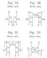
- FIGs. 2A through 2D Prior art level restoration circuits are illustrated in FIGs. 2A through 2D.
- the circuit of FIG. 2A is a level restoration circuit which is used in a complementary pass-transistor logic (CPL).
- Level restoration block of the CPL is constituted with CMOS invertors.
- this CPL level restoration block for example, when a strong or full low level signal (ie ground level signal V SS ) is applied to an input terminal IN thereof, PMOS transistor of the first invertor is made conductive. The strong high level signal V DD is then outputted from an output terminal of the level restoration block (ie the output terminal OUT of the first invertor).
- a weak high level signal V DD -V TN is applied to the other input terminal IN of the level restoration block, NMOS transistor of the second invertor is made conductive so that the weak high level signal is outputted from the other output terminal of the level restoration block (ie the output terminal OUT of the second invertor).
- the CPL level restoration block So as to solve the above mentioned problems of the CPL level restoration block, several circuits such as PMOS latched type CPL, standalone type and SRPL (swing restored pass-transistor logic) level restoration circuits, as shown in FIGs. 2B to 2D, have been proposed.
- the SRPL level restoration circuit is constituted with only CMOS invertors similarly to the CPL level restoration circuit of FIG. 2A.
- one input terminal IN of the level restoration block is commonly connected to the output terminal OUT of the first invertor, and the input terminal of the second invertor, and the other input terminal IN thereof is commonly connected to the output terminal OUT of the second invertor and the input terminal of the first invertor.
- SRPL level restoration circuit for example, when a weak high level signal V DD -V TN from the functional block 2 is applied to the input terminal thereof, the weak high level signal is outputted via one output terminal (ie an output terminal OUT of the first invertor) of the level restoration circuit.
- the weak high level signal is also applied to the input terminal of the second invertor, and thereby the NMOS transistor of the second invertor is turned on.
- the other terminal of the level restoration block ie the output terminal OUT of the second invertor
- the SRPL level restoration circuit is excellent in restoring a weak high level signal to V DD level, but the output voltage thereof is discharged through the NMOS transistors of the functional block 2.
- the discharging time is largely lengthened. This leads to the increase in delay time.
- the multiplier is constructed using Booth's algorithm and Wallace's tree.
- the multiplier has a Wallace's tree compressor 14 which is constituted with a modified Booth's encoder (MBE) 12 and a number of 4-to-2 compressors, and a 108-bit conditional sum adder (CSA) 16.
- This adder 16 is called a conditional carry selection adder or a carry lookahead adder.
- the Wallace's tree compressor 14 is constituted with fifty-four compression units. Fifty -four vertical data signals from the modified Booth's encoder 12 are provided to the fifty-four compression units, respectively. Each vertical data signal which has 32-bit partial product is finally compressed to a 1-bit carry signal and a 1-bit sum signal by means of a corresponding compression unit.
- multiplier Since the above stated multiplier has an encoder to which Booth's algorithm is implemented so as to produce vertical data signals, however, hardware structure of the multiplier is complicated.
- FIG. 4A shows a pass-transistor multiplexer which is used in both the 4-to-2 compressor and the 108-bit conditional sum adder
- FIG. 4B is a detailed circuit diagram of the pass-transistor multiplexer of FIG. 4A.
- this multiplexer of FIG. 4B when a control signal S is at low level, a data signal D0 is selected. When the control signal S is at high level, a data signal D1 is selected. The output signal of the multiplexer is used as an input signal of a next stage multiplexer.
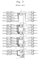
- FIG. 5 shows the 108-bit conditional sum adder of FIG. 3.
- the prior art 108-bit conditional sum adder has fourteen half adder blocks (HA), a first group of first carry lookahead adder blocks (CLA1's), a second group of second carry lookahead blocks (CLA2's), three multiplexers (MUX's) and fourteen conditional sum selection blocks (CSS's).
- the first group of first carry lookahead adder blocks has fourteen carry lookahead adder blocks and the second group of second carry lookahead adder blocks has seven carry lookahead adder blocks.
- One half-adder (HA) and one (CLA1) of the first carry lookahead adder blocks constitute one 8-bit moduled conditional carry selection block.
- One example of the second carry lookahead adder blocks is shown in Fig 7.
- each input signal of the conditional sum adder is delayed by t MUX by means of the half-adder, by 4t MUX by means of the first lookahead adder block CLA1, by 3t MUX by means of the second lookahead adder block CLA2, by 3t MUX by means of the serially connected three multiplexers, and by t MUX by means of the conditional sum selection block CSS.
- Critical path as stated above is caused by simultaneously generating the sum signal and the carry signal. Since carry propagation time is lazy in comparison with sum propagation time, the operation speed of the conditional sum adder is consequently determined by the carry propagation signal.
- a first aspect of the present invention provides an N-bit conditional sum adder comprising:
- a second aspect of the present invention provides an N-bit conditional sum adder comprising:
- a third aspect of the present invention provides an integrated pass-transistor logic circuit comprising:
- FIG. 8 shows a level restoration circuit of EEPL (energy economised pass transistor logic) according to a preferred embodiment of the present invention.
- the level restoration circuit has two CMOS invertors 80 and 84 (hereinafter, referred to as "first invertor” and “second invertor”, respectively), and a regenerative feedback generator 84 which is connected between the input and output of the first and second invertors 80 and 82.
- the regenerative feedback generator 84 is constituted with two PMOS transistors 94 and 96.
- the PMOS transistor 94 has a gate which is connected to a first input 86 (ie, the input of the first invertor 80), and a current path which is connected between a first output 88 (ie, the output of the first invertor 80) and a second input 90 (ie, the input of the second invertor 82).
- the PMOS transistor 96 has a gate which is connected to the second input 90, and a current path which is connected between the first input 86 and a second output 92 (ie, the output of the second invertor 82).
- the current path of each PMOS transistor is also called a source-drain channel.
- a complementary signal IN of the input signal IN when an input signal IN of low level is applied to the first input 86, a complementary signal IN of the input signal IN must be at high level. On the contrary, when the input signal IN is at high level, the complementary signal IN must be at low level.
- a high level signal provided from NMOS functional block 2 is a weak high level signal (V DD -V TN ), as mentioned above.
- the second input signal IN as being a complementary signal thereof is at strong low level V SS and thereby the PMOS transistor of the second invertor 82 is completely turned on.
- the second output 92 is then at strong high level V DD , and the PMOS transistor 96 of the generative feedback generator 84 is made conductive by the second input signal IN of strong low level.
- the second output signal OUT having strong high level V DD is applied to the first invertor 80 as a positive feedback signal. Therefore, the PMOS transistor of the first invertor 80 is completely turned off (or, made nonconductive) so that no leakage current flows through the PMOS transistor. Also, the NMOS transistor of the first invertor 80 is completely turned on (or, made conductive) so that the first output 88 is at strong low level V SS .
- the second input signal IN is a weak high level signal (V DD -V TN )
- the first input signal IN as being a complimentary signal thereof is at strong low level V SS and thereby the PMOS transistor of the first invertor 80 is completely turned on.
- the first output 88 is then at strong high level V DD and the PMOS transistor 94 of the generative feedback generator 84 is made conductive by the first input signal IN of strong low level.
- the first output signal OUT having strong high level V DD is applied to the second invertor 82 as a positive feedback signal. Therefore, the PMOS transistor of the second invertor 82 is completely turned off so that no leakage current flows through the PMOS transistor.
- the NMOS transistor of the second invertor 82 is completely turned on so that the second output 92 is at strong low level V SS .
- the level restoration circuit according to the present invention since the level restoration circuit according to the present invention further has two PMOS transistors 94 and 96 constituting the regenerative feedback generator 84 in comparison with the prior art level restoration circuit FIG. 2A, it may be some increased in chip area. But, the chip area of the level restoration circuit can be largely reduced because the two PMOS transistors 94 and 96 are used for switching.
- the lay-out size of the level restoration circuit is some larger than that of the prior art CPL (complementary pass-transistor logic), and nearly the same as that of another prior art CPL2.
- the table 1 shows characteristics of full adders with level restoration circuits to which the prior art and the present invention are implemented under the conditions that 0.6 ⁇ m CMOS technique is applied to fabricate the same, a source power V SS is set to 3.3V, and a load capacitance C L is set to 30fF.
- FIG. 9 shows a 1-bit full adder which has a level restoration block 4A and a functional block 2A according to the present invention.
- a reference symbol A indicates a most significant bit (MSB) and C does a least significant bit (LSB).
- MSB most significant bit
- LSB least significant bit
- Two low-order bits of the input signals B and C, and complementary signals B and C thereof are provided to a first addition section 100 of the functional block 2A to be added. Partial sum signal P and complementary signal P of the first addition section 100, as well as the MSB signal A and the complementary signal A thereof are provided to the second addition section 102 to be added.
- Sum signal Q and complementary signal Q from the second addition section 102 are provided to an EEPL level restoration circuit 104 in the level restoration block 4A, and are restored to full levels by the EEPL level restoration circuit 104 to be outputted as a final sum signal SUM and a complementary signal SUM thereof.
- a fifth addition section 110 performs the addition of a partial sum signal R of the third addition section 106, a complementary signal R of the partial R, the other partial sum signal S of the third addition section 106, a complementary signal S of the partial sum signal S, the MSB signal A and the complementary signal A of the MSB signal to output a carry signal T and a complementary signal T thereof.
- the signals T and T from the fifth addition section 110 are provided to the EEPL circuit 112 of the level restoration block 4A, and restored to full levels by the EEPL level restoration circuit 104 to be outputted as both a final carry signal CARRY and a complementary signal CARRY thereof.
- FIG. 10A shows ideal simulation environment of the 1-bit full adder shown in FIG. 9.
- PxD power consumption
- FIG. 10B is a waveform diagram of input and output signals of the full adder shown in FIG. 10A.
- reference symbols A, B and C all indicate the input signals of the full adder, respectively.
- a reference symbol SUM indicates the sum signal and a reference symbol CARRY does the carry signal.
- FIG. 11 shows the simulation environment of a cascade full adder chain
- FIGs. 12 and 13 show graph diagrams showing an average delay characteristic of the pass-transistor logic in the full adder chain shown in FIG. 11, and a power consumption characteristic of the pass-transistor logic in the full adder chain shown in FIG. 11, respectively.
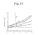
- FIG. 15 is a graph diagram showing power (P)xdelay(D) characteristic of the respective pass-transistor logic in the full adder chain shown in FIG. 11.
- an x-axis indicates the relative ratio (m) of W(width)/L(length) of the function block
- reference symbols 'a' through 'e' indicate CPL, CPL2, Standalone, SRPL and EEPL of the present invention.
- a delay is increased in proportion to the relative ratio of W/L, and that the delay of the EEPL according to the present invention is shortened as compared with that of the prior art CPL or the prior art SRPL.
- the prior art SRPL is not nearly operated when the W/L ratio thereof is small, or when transistor size is small.
- the prior art SRPL is normally operated only when being fabricated in proportion to three or four times of the basic W/L ratio. Therefore, the SRPL structure is not preferable in the light of the reduction of chip area.
- FIG. 16 shows a (54x54)-bit multiplier according to the present invention.
- the (54x54)-bit multiplier an encoder 114 for producing fifty-four vertical data signals each of which has fifty-four bits, a Wallace's tree compressor 116 for compressing each 54-bit vertical data signal into a 2-bit signal, for example a carry signal and a sum signal, and a 108-bit conditional sum adder 118 for generating a multiplication result by adding the sum signals, with propagating the carry signals.
- the encoder 114 which constituted with a plurality of multiplexers is provided to receive a 54-bit multiplier signal and a 54-bit multiplicand signal, and to produce the fifty-four 54-bit vertical data signals.
- a bit value of the 54-bit multiplicand signal is '1', a bit value of the 54-bit multiplier is directly outputted.
- a bit value of the 54-bit multiplicand signal is '0', a bit value is set to '0' to be outputted.
- An n-th vertical data signal becomes equal to a partial product of the 54-bit multiplier signal and an n-th bit value of the 54-bit multiplicand signal, where n is 1, 2,..., 54. Consequently, fifty-four partial products corresponding to the multiplicand signal of MSB to LSB are produced as the fifty-four vertical data signals.
- the following table 2 illustrates the production of the vertical data signals in case of a (4x4) multiplier.
- the first to fourth vertical data signals are produced as '1101', '0000', '0000' and '1101' in accordance with respective bit values of the multiplicand data.
- the first and fourth vertical data signals which correspond to the MSB and LSB of the multiplicand data whose both bit values are '1', have the same data as the multiplier data '1101'.
- the second and third vertical data signals which correspond to the other bits of the multiplicand data whose both bit values are '0', have '0000'. All the vertical data signals are provided to the Wallace's tree compressor 116.
- the Wallace's tree compressor 116 is constituted with fifty-four compression units 120 corresponding to the fifty-four vertical data signals.
- Each compression unit has six 9-to-2 compressors, two 6-to-2 compressors and a 4-to-2 compressor.
- the 54-bit vertical signal from the encoder 114 is divided in 9-bit signals to be provided to the six 9-to-2 compressors.
- Each 9-to-2 compressor compresses a corresponding 9-bit signal and produce a 2-bit signal, ie carry and sum signals.
- 12-bit data signal from the six 9-to-2 compressors is divided in 6-bit signals to be provided to the two 6-to-2 compressors.
- 4-bit data signal from the 6-to-2 compressor is provided to the 4-to-2 compressor.
- the Wallace's tree compressor 116 With this construction of the Wallace's tree compressor 116, a single compressor produces a 2-bit data, ie a carry and a sum signal, and thus the compressor 116 can produce a 108-bit data signal.
- the 108-bit data signal from the Wallace's tree compressor 116 is provided to the 108-bit conditional sum adder 118.
- FIG. 20 an example of the compression unit 120 is illustrated.
- the 108-bit carry and sum signals from the fifty-four compression units related to the fifty-four vertical data signal have the same delay time and are provided to the conditional sum adder 118.
- a (54x54)-bit multiplication data is finally produced by the conditional sum adder 118.
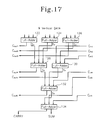
- FIG. 17 shows one of the 9-to-2 compressors of FIG. 16.
- each of the 9-to-2 compressors has seven full adders 122 ⁇ 134, each of which has the same construction as the full adder of FIG. 9.
- the 9-to-2 compressor receives a 9-bit data of the 54-bit vertical data provided from the encoder 114 and a six bit carry signal C in1 ⁇ C in6 provided from a k-th 9-to-2 compressor of an (n-1)-th compression unit, and produces a carry bit signal CARRY, a sum bit signal SUM and the other carry bit signals C out1 ⁇ C out6 to be provided to a corresponding compressor, ie the k-th 9-to-2 compressor of a (n+1)-th compression unit.
- the 9-bit vertical data signal from the encoder 144 is divided in 3-bit signals, which are respectively provided to a first to a third full adders 122, 124 and 126. These full adders then produce a first to a third sum bit signals S 1 ⁇ S 3 and a first to a third carry bit signals C out1 ⁇ C out3 to be provided to the k-th 9-to-2 compressor of a next stage compression unit, ie the (n+1)-th compression unit.
- the fourth full adder 128 receives the first to the third sum bit signals S 1 ⁇ S 3 and produces a fourth sum bit signal S 4 and a fourth carry bit signal C out4 to be provided to the k-th 9-to-2 compressor of the next stage compression unit.
- the fifth full adder 130 receives the first to the third carry bit signals C in1 ⁇ C in3 from a pre-stage compression unit, ie the (n-1)-th compression unit and produces a fifth sum bit signal S 5 and a fifth carry bit signal C out5 to be provided to the k-th 9-to-2 compressor of the next stage compression unit.
- the sixth full adder 132 receives the fourth and fifth sum bit signals S4 and S5 and the fifth carry bit signal C in4 from a corresponding 9-to-2 compressor of the pre-stage compression unit and produces a sixth sum bit signal S 6 and a sixth carry bit signal C out6 to be provided to a corresponding 9-to-2 compressor of the next stage compression unit.
- the seventh full adder 134 receives the sixth sum bit signal S 6 from the sixth full adder and the fifth and sixth carry bit signals C in5 and C in6 from the pre-stage compression unit and finally produces the sum bit signal SUM and the carry bit signal CARRY.
- FIG. 18 shows one of the two 6-to-2 compressors of FIG. 16.
- Each of the two 6-to-2 compressors has four full adders 136, 138, 140 and 142, each of which has the same construction as the full adder of FIG. 9.
- each of the two 6-to-2 compressors receives a 6-bit data of the 12-bit vertical data signal from the six 9-to-2 compressors and a 3-bit carry signal C in1 ⁇ C in3 from a first 6-to-2 compressor of the pre-stage compressor unit, ie the (n-1)-th compression unit, and generates the carry bit signal CARRY, the sum bit signal SUM and the other carry bit signals C out1 ⁇ C out3 to be provided to a corresponding 6-to-2 compressor of the next-stage compression unit, ie the (n+1)-th compression unit.
- the 6-bit vertical data signal from three corresponding 9-to-2 compressors is divided in 3-bit signals to be provided to the first and second full adders 136 and 138.
- These full adders 136 and 138 then produce first and second sum bit signals S 1 and S 2 as well as first and second carry bit signals C out1 and C out2 to be provided to a first 6-to-2 compressor of the next stage compression unit, ie the (n+1)-th compression unit.
- the third full adder 140 receives the first to the third carry bit signals C in1 ⁇ C in3 from a corresponding 6-to-2 compressor of the pre-stage compression unit, and produces a third sum bit signal S 3 and a third carry bit signal C out3 to be provided to the first 6-to-2 compressor of the next stage compression unit.
- the fourth full adder 142 receives the first to the third sum bit signals S 1 ⁇ S 3 from the first to third full adders and finally produces the sum bit signal SUM and the carry bit signal CARRY.
- FIG. 19 shows the 4-to-2 compressor of FIG. 16.
- the 4-to-2 compressor has two full adders 144 and 146, each of which has the same construction as the full adder of FIG. 9.
- the 4-to-2 compressor receives a 4-bit vertical data signal from the two 6-to-2 compressors and a 1-bit carry signal C in1 from a corresponding 4-to-2 compressor of the pre-stage compressor unit, ie the (n-1)-th compression unit, and generates the carry bit signal CARRY, the sum bit signal SUM and the other carry bit signal C out1 to be provided to a corresponding 4-to-2 compressor of the next-stage compression unit.
- a low-order 3-bit signal of the 4-bit vertical data signal from two corresponding 6-to-2 compressors is provided to the first full adder 144 which produces a first sum bit signal S 1 as well as a carry bit signal C out1 to be provided to the 4-to-2 compressor of the next stage compression unit.
- the second full adder 140 receives the MSB of the 4-bit vertical data signal, the sum bit signal S 1 from the first full adder 144 and the carry bit signal C in1 from the 4-to-2 compressor of the pre-stage compression unit, and produces final sum and carry bit signals SUM and CARRY.
- the sum and carry bit signals produced thus are supplied to the 108-bit conditional sum adder 116, as shown in FIG. 16.
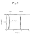
- FIG. 21 shows simulation results of a threshold path in the compression unit according to the present invention. From this FIG., it can be seen that the time of about 8.34 nanoseconds is required to obtain an output from an input.
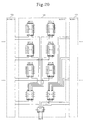
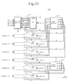
- FIG. 22 shows the 108-bit conditional sum adder circuit of FIG. 16 according to a preferred embodiment of the present invention.
- the 108-bit conditional sum adder 118 as shown in FIG. 22, is constituted with seven moduled 16-bit sum generation blocks 150-1 ⁇ 150-7, and two 4-bit carry generation blocks 160-1 and 160-2.
- Each of the sum generation blocks 150-1 ⁇ 150-7 has a pre-carry&pre-sum generator 152 and a 16-bit conditional sum adder 154.
- the sum generation blocks are constituted with EEPL and the carry generation blocks with CMOS logic.
- conditional sum adder 118 it is the most significant feature of the 108-bit conditional sum adder that, before carry propagation which is generated through multiplexer chain in respective sum generation blocks 150-1 ⁇ 150-7 arrives at the final stage of the multiplexer chain, the final stage is driven by block carry signals BC i and BC i provided from the respective carry generation blocks 160-1 and 160-2.
- the carry generation and the sum generation occur simultaneously in the prior art conditional sum adder, but individually in the conditional sum adder 118 according to the present invention. Therefore, the conditional sum adder 118 of FIG. 22 can achieve an improved operation speed. Namely, the conditional sum adder 118 has a shorten delay time of about 2t MUX in comparison with the prior art conditional sum adder.
- the 108-bit conditional sum adder 118 has a faster operation speed and a lower power dissipation, as compared with the prior art conditional sum adder having either the pass-transistor logic or the CMOS logic.
- the respective pre-carry&pre-sum generators 152 in the first to sixth sum generation blocks, 150-1 ⁇ 150-6 receive a first 16-bit input signal A i ⁇ A i+15 (where "I" is equal to 0, 16, 32 ..., 80), a complementary signal ( A i ⁇ A i+15 of the first 16-bit input signal, a second 16-bit input signal B i ⁇ B i+15 and a complementary signal B i ⁇ B i +15 of the second 16-bit input signal, and generate a first 16-bit conditional sum signal SH, a second 16-bit conditional sum signal SL, a first 16-bit conditional carry signal CH or P, a complementary signal CH of the first 16-bit conditional sum signal SH, a second 16-bit conditional carry signal CL or G, and a complementary signal CL of the second 16-bit conditional carry signal.
- the pre-carry&pre-sum generator 152 in the seventh sum generation block receives a first 12-bit input signal A 96 ⁇ A 107 , a complementary signal A 96 ⁇ A 107 of the first 12-bit input signal, a second 12-bit input signal B 96 ⁇ B 107 and a complementary signal B 96 ⁇ B 107 of the second 16-bit input signal, and generates a first 12-bit conditional sum signal SH, a second 12-bit conditional sum signal SL, a first 12-bit conditional carry signal CH or P, a complementary signal CH of the first 12-bit conditional carry signal CH, a second 12-bit conditional carry signal CL or G, and a complementary signal CL of the second 12-bit conditional carry signal.
- the conditional sum adder 154 receives several signals from the pre-carry&pre-sum generator 152, ie the first conditional sum signal SH, the second conditional sum signal SL, the first conditional carry signal P, the complementary signal CH of the first conditional sum signal SH, the second conditional carry signal G, and the complementary signal CL of the second conditional carry signal.
- the first to sixth 16-bit conditional sum adders of the seven sum generation blocks 150-1 ⁇ 150-7 generates a first to sixth 16-bit sum signals S i ⁇ S i+15 (where "I" is 0, 16, 32,..., 80) and the seventh 16-bit conditional sum adder thereof generates a seventh 16-bit sum signal S 96 ⁇ S 107 .
- the first and second conditional carry signals P and G from the pre-carry&pre-sum generators 154 are applied to the first carry generation block 160-1.
- the first and second conditional carry signals P and G from the pre-carry&pre-sum generators 154 are applied to the second carry generation block 160-2.
- the first and second conditional carry signals P and G indicate carry propagation and carry generation signals, respectively.
- the first carry generation block 160-1 generates first to fourth block carry signals BC 0 ⁇ BC 3 and complementary signals BC 0 ⁇ BC 3 thereof, all of which are provided to the second sum generation block 150-2.
- Second block carry signal BC 1 and the complementary signal BC 1 thereof are provided to the third sum generation block 150-3.
- Third block carry signal BC 2 and the complementary signal BC 2 thereof are provided to the fourth sum generation block 150-4.
- Fourth block carry signal BC 3 and the complementary signal BC 3 thereof are provided to the fifth sum generation block 150-5 and the second carry generation block 160-2.
- Each of the block carry signals is a 1-bit signal.
- the second generation block 160-2 generates the fifth to seventh block carry signals BC 4 ⁇ BC 6 and the complementary signals BC 4 ⁇ BC 6 thereof.
- the fifth block carry signal BC 4 and the complementary signal BC 4 thereof are supplied to the sixth sum generation block 150-6.
- the seventh block carry signal BC 6 and the complementary signal BC 6 are generated as the final carry and complementary signals C out and C out , respectively.
- the 108-bit conditional sum adder deals with the carry generation and the sum generation separatively, so that the operation speed thereof can be improved faster. That is, the delay time of the sum generation block is 10t MUX which is comprised of, for example, t MUX due to the pre-carry&pre-sum generator 152, 8t MUX due to the 16-bit conditional sum adder 154 and t MUX due to the block carry signals BC j and BC J (or C IN and C IN from the carry generation block 160-1 or 160-2.
- the delay time due to the carry generation blocks 160-1 and 160-2 is, it is not exceeded by 8t MUX .
- the delay time due to the carry generation block is shortened in comparison with that of the sum generation block. Accordingly, the carry propagation time is faster than the sum propagation time so that addition speed is performed relatively fast.
- the 108-bit conditional sum adder has seven sum generation blocks 150-1 ⁇ 150-7, ie seven 16-conditional sum adders.
- This (7x16) adder structure has a lower delay time, as compared with a prior art (8x14), (12x9) or (29x6) adder structure.
- the delay time of the sum generation block is 5t MUX which is comprised of t MUX due to the pre-carry&pre-sum generator and 4t MUX due to the sum generator (where t MUX is a delay time due to one multiplexer).
- the delay time due to the carry generation block is about 12t MUX even though the block is implemented with group carry and group sum methods.
- the 108-bit conditional sum adder having a prior art (8x14) adder structure has at least 12t MUX of delay time.
- the delay times of respective adder structures are illustrated by the following Table 3.
- Adder Structure Delay Time of Sum Generation Block (t MUX ) Delay Time of Carry Generation Block (t MUX ) Total Delay Time (t MUX ) 8x14 5 11 12 12x9 7 10 11 7x16 9 9 10 20x6 11 10 12
- the (7x16) adder structure according to the present invention has the most short delay time in total, as compared with the other prior art adder structures.
- FIG. 23 is a detailed circuit diagram of a pre-carry&pre-sum generator according to this embodiment.
- the generator 152 includes sixteen pre-carry & pre-sum generation units.
- Each of the generation units three function blocks 162, 164 and 166, and two EEPL level restoration blocks 168 and 170.
- First function block 162 includes two NMOS transistors 172 and 174 for XNORing inputs A and B, and two NMOS transistors 176 and 178 for XORing inputs A and B.
- Second function block 164 is composed of two NMOS transistors 180 and 182 for NORing inputs A and B, and two NMOS transistors 184 and 186 for ORing inputs A and B.
- Third function block 166 is composed of two NMOS transistors 190 and 192 for NANDing inputs A and B, and two NMOS transistors 192 and 194 for ANDing inputs A and B.
- first EEPL level restoration block 168 Two output terminals of the second function block 164 are connected with first EEPL level restoration block 168, those of the third function block 166 is connected with second EEPL level restoration block 170.
- Each level restoration block includes two invertors and two PMOS transistors. Specifically, in first level restoration block 168, input terminal of invertor 196 is connected to output terminal 181 of NOR logic, and CH (or P) is outputted from output terminal of the invertor 196. Input terminal of invertor 198 is connected to output terminal 183 of NOR logic, and CH (or P ) is outputted from output terminal of the invertor 198.
- invertor 204 input terminal of invertor 204 is connected to output terminal 189 of NAND logic, and CL (or G) is outputted from output terminal of the invertor 204.
- Input terminal of invertor 206 is connected to output terminal 193 of AND logic, and CL (or G ) is outputted from output terminal of the invertor 206.
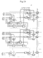
- FIG. 24 is a detailed circuit diagram of 16-bit conditional sum adder.
- the adder 154 includes a plurality of multiplexers.
- LRB represents the EEPL level restoration circuit of FIG. 8
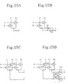
- MSL, MD and MDL represent pass-transistor multiplexers of FIGs. 25A to 25D, respectively.
- MS denotes a single multiplexer selectively outputting one of two data D0 and D1 in accordance with two complementary inputs IN and IN .
- the MS has two NMOS transistors 240 and 242.
- MSL is a single multiplexer with level restoration circuit, and it outputs the converted signal of one of two data. This MSL, as shown in FIG.
- MD is a dual multiplexer which selectively outputs one of two data and one of its complementary data in accordance with two complementary inputs.
- the MD includes four NMOS transistors 250, 252, 254 and 256, as shown in FIG. 25C.
- MDL is a dual multiplexer with level restoration circuit, and it outputs inverted signals of outputs of the dual multiplexers.
- the MDL as shown in FIG. 25D, includes four NMOS transistors 258, 260, 262 and 264, and EEPL level restoration circuit 266.
- the EEPL level restoration circuit 266, as described before, includes two invertors 270 and 272, and two PMOS transistors 274 and 276.
- 16-bit conditional sum adder 154 includes eight conditional sum units 210-1 ⁇ 210-8.
- First conditional sum unit 210-1 receives first conditional sum signals SH and second conditional sum signals SL, first conditional carry signals CH (or P) and second conditional carry signals CL (or G), and 2-bit lower order signals SH i and SH i+1 , SL i and SL i+1 , CH i and CH i+1 , CH i and CH i+ 1 , CL i and CL i+1 , CL i and CL i +1 of respective complementary signals CL of the second conditional carry signals which are provided from corresponding pre-carry & pre-sum generator 152, and generates 2-bit sum signals S i and S i+1 .
- Second conditional sum unit 210-2 receives next 2-bit signals SH i+2 and SH i+3 , SL i+2 and SL i+3 , CH i+2 and CH i+3 , CH i +2 and CH i+ 3 , CL i+2 and CL i+3 , CL i+2 and CH i +3 from the corresponding pre-carry & pre-sum generator 152, and generates next 2-bit sum signals S i+2 and S i+3 .
- first through eight conditional sum adder units 210-1 ⁇ 210-8 produces 16-bit sum signals S i ⁇ S 1+15 .
- Each conditional sum adder unit includes two LRBs 212 and 224, six Mss 214, 216, 220, 222, 226 and 228, two MSLs 218 and 230, two MDS 232 and 234 and two MDLs 236 and 238.
- input terminals IN and IN of first LRB 212 is supplied with lower order bit SH signal and lower order bit SL signal, respectively.
- the levels of the signals SH and SL are respectively restored to the full levels i.e., V.D. and Vss (GND) by means of first LRB 212.
- the full level signals SH and SL from output terminals OUT and OUT of the LRB 212 are provided to input terminals D0 and D1 of MS 214, respectively.
- Each of Mss 214 and 216 selectively outputs one of two inputs in response to selection signals.
- select terminals IN and IN of the MS 214 are supplied with control signals of V.D. and GND levels, respectively, and select terminals IN and IN of the MS 216 are supplied with control signals of GND and V.D. levels, respectively. Therefore, the MS 214 outputs signal SH, and the MS 216 outputs signal SL.
- the signals SH and SL from Mss 214 and 216 are applied to input terminals D1 and D0 of MSL 218, respectively.
- the MSL 218 outputs the converted signal of the signal SL from the MS 216, i.e., full high level signal as a least significant bit sum signal Si when a control signal C IN is at V.D. level.
- the MSL outputs the converted signal of the signal SH from the MS 214, i.e, full low level signal as the least significant bit sum signal Si when a control signal C IN is at V.D. level.
- the input terminals D1 and D0 of the MS 220 are supplied with upper order bit SH signal and upper order bit SL signal, respectively.
- the input terminals D1 and D0 of the MS 222 are also supplied with the upper order bit SH signal and the upper order SL signal, respectively.
- the select terminals IN and IN of the MS 220 are provided with lower order bit signals CH(i.e., P) and CH (i.e., P ), respectively, and the select terminals IN and IN of the MS 222 are respectively provided with lower order bit signals CL (i.e., G) and CL (i.e., G ). Since the signals CH and CL are high and the signals CL and CH are low, the MSs 220 and 222 output signals SL and SH, respectively.
- the signals SL and SH are applied to the input terminals IN and IN of the LRB 224, respectively. Signals SH and SL of full levels are thus outputted from output terminals OUT and OUT of the LRB 224, respectively.
- Input terminals D0 and D1 of the MS 226 are supplied with the signals SH and SL from the LRB 224, respectively.
- the signals SH and SL are also provided to the input terminals D0 and D1 of the MS 228, respectively.
- Each of the Mss 226 and 228 outputs one of two inputs selectively, in response to select signals.
- the select terminals IN and IN of the MS 226 are supplied with control signals of V.D. and GND levels, respectively, and the select terminals IN and IN of the MS 228 are supplied with control signals of GND and V.D. levels, respectively.
- the MS 226 outputs signal SH
- the MS 228 outputs signal SL.
- the signal SH from the fifth MS 226 and the signal SL from the sixth MS 228 are provided with input terminals D1 and D0 of the second MSL 230.
- the second MSL 230 outputs the inverted SL signal, ie a strong high level signal, as a Summation signal S I+1 when the level of the control signal C IN provided to its selection terminal IN is same as V D0 level.
- the second MSL 230 outputs the inverted SH signal, ie, a stron low level signal, as a Summation signal S i+1 when the level of the control signal C IN provided to its selection terminal IN is same as V.D. level.
- the upper order bit CH signal and its inverted signal CH , and the lower order bit CL signal and its inverted signal CL are supplied with the input terminals D0, DO , D1, D1 of the first and second MDs 232 and 234.
- the lower order bit CH(P) signal and the lower order bit CH ( P ) signal are supplied with the input terminals IN and IN of the first MD 232.
- the lower order bit CL (G) signal and the lower order bit CL ( G ) are supplied with input terminals IN , IN of the second Mds 234. Since each CH and CL signals has high levels and each CL and CL signals is low levels, the first MD 232 outputs CL and CL signals and the second MD 234 outputs CH and CH signal.
- CL, CL , CH, and CH signals from the first and second MDs 232, 234 are supplied into input terminals D1, D1 , DO, D0 of the first and second MDLs 236 and 238, respectively.
- Each of the first and second MDLs 236 and 238 outputs the one of its input signals and inverted input signals selectively in response to its selection signals.
- a selection signal of V.D. level and a selection signal of GND level are input into the select terminals IN and IN of the second MDL 238, respectively.
- the first MDL 236 selects and outputs signals CH and CH each of which is inverted from the signal CL and CL , respectively
- the second MDL 238 selects and outputs signals CL and CL each of which is inverted fro the signal CH and CH , respectively.
- the signals CH, CH , CL, CL from the first and second MDLs 236 and 238 are provided as a control signal with the multiplexers within the next conditional summation unit.
- the delay time of 16 bits adder 154 is 8t mux . Compared with that of conventional one, this represents 56% improvements.
- FIG. 27 shows carry generation block 160-1 schematically.
- carry generation block 160-1 comprises five CLA sections 300-1 ⁇ 300-4 and 310.
- the first to fourth CLA sections 300-1 ⁇ 300-4 have same structure with each other but the fifth CLA section 310 has different structure.
- Each of the first to fourth CLA sections 300-1 ⁇ 300-4 has five CLA1 adders 302-1 ⁇ 302-5 and the fifth CLA section has a CLA2 adder which has different structures.
- 16 bits G signals and 16 bits P signals from corresponding pre-charge and pre-sum generator 152 are separated by 4 bits and supplied respectively with CLA1 adders 302-1 ⁇ 302-4.
- signals P0 ⁇ P3 and G0 ⁇ G3 are supplied with CLA1 adder 302-1 and signals P4 ⁇ P7 and G4 ⁇ G7 are supplied with CLA1 adder 302-2 and signals P8 ⁇ P11 and G8 ⁇ G11 are supplied with CLA1 adder 302-3 and signals P12 ⁇ P15 and G12 ⁇ G15 are supplied with CLA1 adder 302-4.
- CLA1 adder 302-1 generates group carry and group carry transfer signals GG0 and GP0 and CLA1 adder 302-2 generates signals GG1 and GP1 and CLA1 adder 302-3 generates signals GG2 and GP2 and CLA1 adder 302-4 generates signals GG3 and GP3, respectively. Furthermore, 8 bits signal GG0 ⁇ GG3 and GP0 ⁇ GP3 from the CLA1 adder 302-1 ⁇ 302-4 are supplied with CLA1 adder 302-5. The CLA1 adder 302-5 generates the first section carry generation signal SG0 and the first section carry transfer signal SP0.
- the second to fourth section carry generation signals SG1 ⁇ SG3 and the second and fourth section carry transfer signals SP1 ⁇ SP3 are generated by the second to fourth CLA sections 300-2 ⁇ 300-4.
- 8-bit signals from the fourth CLA sections 300-1 ⁇ 300-4 that is, signals SG 0 ⁇ SG 3 and SP 0 ⁇ SP 3, are provided by the fifth CLA section 310.
- the fifth CLA section 310 generates first to fourth block carry signals BC 0 ⁇ BC 3, and their complementary signals BC 0 ⁇ BC 3 .
- the fifth CLA section within the second carry generation block 160-2 generates first to third block carry signals BC 4 ⁇ BC 6, and their complementary signals BC 4 ⁇ BC 6 .
- FIG. 28A and FIG. 28B are detailed circuit diagrams showing group carry generation section of each CLA1 adders and group carry propagation.
- the group carry generation and group carry propagation sections are consisted of the CMOS logic, by contrast with the sum generation block consisted of pass-transistor, in order to improve the operating speed of 108 bits adder. This is intended for reducing carry propagation delay caused by pass-transistor multiplexer.
- the group carry generation of CLA1 adder includes seven PMOS transistors 330 ⁇ 342, ten NMOS transistors 344 ⁇ 362, and an invertor 364.
- a current path of PMOS transistor is connected between source voltage V.D. and the node N331, and signal G 0 is provided to the gate thereof.
- Current paths of PMOS transistors 332, 336 and 340 are connected between source voltage V.D. and the node N335, N339 and N341, and signals P 1 ⁇ P 3 are provided to the gate thereof.
- a current path of PMOS transistor 334 is connected between the current paths of PMOS transistors 330, 332 and the node N331, and signal G 1 is provided in the gate of PMOS transistors 334.
- a current path of PMOS transistor 338 is connected between the current paths of PMOS transistors 334, 336 and the node N335, and signal G 2 is provided to the gate of PMOS transistor 338.
- a current path of PMOS transistor 342 is connected between the current paths of PMOS transistors 338, 340 and the node N341, and signal G 3 is provided to the gate of PMOS transistor 342.
- NMOS transistors 344, 352, 354 and 356 are connected in series between the ground voltage GND and the node N341, and signals G 0 and P 1 ⁇ P 3 are provided to gates of NMOS transistors 344, 352 and 354.
- Current paths of NMOS transistors 346, 358 and 360 are connected in series between the ground voltage GND and the node N341, and signals G 1 , P 2 and P 3 are provided to gates of NMOS transistors 346, 358 and 360.
- Current paths of NMOS transistors 348 and 362 are connected in series between the ground voltage GND and the node N341, and signals G 2 and P 3 are provided to gate of NMOS transistors 348 and 362.
- a current path of NMOS transistor 350 is connected in series between the ground voltage GND and the node N341, and signals G 3 is provided to gate of NMOS transistor 350.
- An invertor 364 inverts a signal generated by PMOS transistors 330 ⁇ 342 and NMOS transistors 344 ⁇ 362 on the node N341, and outputs a signal of group carry generation GG.
- group carry propagation of CLA1 is consisted of four PMOS transistors 366 ⁇ 372, four NMOS transistors 374 - 380 and an invertor 382.
- Current paths of PMOS transistors 366 ⁇ 372 are connected in mutual parallel between source voltage V.D. and the node N373.
- Current paths of NMOS transistors 374 ⁇ 380 are connected in series between the reference voltage, that is, ground voltage GND and the node N373.
- An invertor 382 inverts a signal generated by PMOS transistors 366 ⁇ 372 and NMOS transistors 374 ⁇ 380 on the node N341, and outputs a signal of group carry propagation GP.
- FIG. 29 is a detailed circuit diagram of CLA2 adder 310 in FIG. 27.
- CLA2 adder 310 includes three CLA1 adders 400-1, 400-2, 400-3 and four MDLs 410, 412, 414, 416.
- Each of the CLA1 adders 400-1, 400-2 and 400-3 shown in FIG. 29 has the same construction as the CLA1 of FIG. 27, and thus detailed description is omitted hereunder.
- the CLA1 adder 400-1 receives SG 0 , SG 1 , SP 0 , and SP 1 signals and produces BG 1 and BP 1 signals.
- the CLA1 adder 400-2 receives SG 0 , SG 1 , SG 2 , SP 0 , SP 1 and SP 2 signals and produces BG 2 and BP 2 signals.
- the CLA1 adder 400-3 receives SG 0 , SG 1 , SG 2 , SG 3 , SP 0 , SP 1 , SP 2 , and SP 3 signals and produces BG 3 and BP 3 signals.
- the SG 0 and SP 0 signals are applied to the inputs D0 and D1 of the MDL 410, and the BG 1 and BP 1 signals from the CLA1 adder 400-1 are applied to the inputs D0 and D1 of the MSL 412.
- the BG 2 and BP 2 signals from the CLA1 adder 400-2 are applied to the inputs D0 and D1 of the MSL 414, and the BG 3 and BP 3 signals from the CLA1 adder 400-3 are applied to the inputs D0 and D1 of the MSL 414.
- C IN and C IN are applied to the selection terminals IN and IN of each of the MDLs 410 ⁇ 416.
- Each MDL 410 ⁇ 416 selects and outputs any of two input signals in response to the C IN and C IN signals.
- the MDLs 410 ⁇ 416 produce block carry signals BC 0 ⁇ BC 3 and complementary signals BC 0 ⁇ BC 3 thereof, as shown in FIG. 29.
- the carry generation block 160-2 has the same construction as the carry generation block 160-1 except that 12-bit carry generation signals and 12-bit carry propagation signals are provided to the fourth CLA section, and descriptions thereof are omitted.
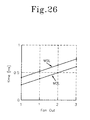
- FIG. 30 shows SPICE simulation results of the 108-bit conditional sum adder according to the present invention. From FIG. 30, it can be seen that the carry propagation is faster than the sum propagation.
- FIG. 31 shows the multiplication times between the prior art multiplier using only 4-to-2 compressors and the multiplier of FIG. 16. As shown in FIG. 31, the multiplication time with respect to threshold path of the multiplier according to the present invention is 13.5 nanoseconds, but the multiplication time of the prior art multiplier is 15.1 nanoseconds. Therefore, it can be understood from FIG. 31 that the multiplication speed of the multiplier according to the present invention is as fast as about 13% of that of the prior art multiplier.
- conditional sum adder in which EEPL circuit is implemented according to the present invention has advantages of low power dissipation, a smaller chip area.
- conditional sum adder deals with carry generation and sum generation separately, and the carry propagation is performed faster than the sum propagation, its operation speed can be improved.
Abstract
Description
| Number of Transistors | Relative Chip Area | Delay [ns] | Power [mW/25MHz] | PowerX Delay [pJ] | Relative Energy Consumption | AreaXEnergy Consumption | |
| CPL (m=1) | 28 | 100 | 1.00 | 0.356 | 0.358 | 100.0 | 100.0 |
| CPL2 (m=1) | 32 | 109 | 0.74 | 0.266 | 0.197 | 40.7 | 44.4 |
| Stand (m=1) | 32 | 109 | 1.08 | 0.297 | 0.321 | 97.0 | 105.8 |
| SRPL (m=3) | 28 | 758 | 0.56 | 0.496 | 0.278 | 43.6 | 330.5 |
| EEPL (m=1) | 32 | 109 | 0.85 | 0.233 | 0.198 | 46.9 | 51.1 |

| Adder Structure | Delay Time of Sum Generation Block (tMUX) | Delay Time of Carry Generation Block (tMUX) | Total Delay Time (tMUX) |
| 8x14 | 5 | 11 | 12 |
| | 7 | 10 | 11 |
| | 9 | 9 | 10 |
| 20x6 | 11 | 10 | 12 |
Claims (32)
- An N-bit conditional sum adder comprising:andK M-bit sum generators, wherein K is equal to |N/M|;X L-bit carry generators, wherein X is equal to |K/L|; in which:each of the M-bit sum generators receives a first M-bit input signal and its complementary signal, a second M-bit signal and its complementary signal, an L-bit carry signal and its complementary signal and is adapted to generate an M-bit sum signal;each of a first to an (X-1)-th of the L-bit carry generators receives a (L×M)-bit carry generation signal and a (L×M)-bit carry propagation signal from a corresponding L M-bit sum generators and is adapted to generate the L-bit carry signal and its complementary signal; andthe X-th L-bit carry generator receives the carry generation and propagation signals from the remaining (K-L×(X-1)) M-bit sum generators and is adapted to generate a carry signal and its complementary signal.
- A conditional sum adder according to claim 1, wherein each of the M-bit sum generators comprises a pass-transistor logic.
- A conditional sum adder according to claim 1 or claim 2, wherein each of the L-bit carry generators comprises a CMOS logic.
- A conditional sum adder according to any preceding claim in which M is 16 and L is four.
- A conditional sum adder according to claim 4 in which K is 7 and X is 2.
- A conditional sum adder according to any preceding claim wherein each of the M-bit sum generators comprises:first means for receiving the first M-bit input signal and its complementary signal and the second M-bit input signal and its complementary signal and for generating a first M-bit conditional sum signal, a second M-bit conditional sum signal, an M-bit carry propagation signal and its complementary signal and an M-bit carry generation signal and its complementary signal; andsecond means for receiving the first M-bit conditional sum signal, the second M-bit conditional sum signal, the M-bit carry propagation signal and its complementary signal, the M-bit carry generation signal and its complementary signal and the L-bit carry signal and its complementary signal for generating the M-bit sum signal.
- A conditional sum adder according to claim 6 in which the first means comprises a (6×M)-bit pre-carry & sum generation block and the second means an M-bit carry lookahead addition block.
- An N-bit conditional sum adder comprising:K M-bit sum generators, each of which receives a first M-bit input signal and its complementary signal, a second M-bit input signal and its complementary signal, an L-bit carry signal and its complementary signal and adapted to generate an M-bit sum signal, wherein K is equal toN/M┐; and
 X L-bit carry generators, each of which receives a (L×M)-bit carry generation signal and a (L×M)-bit carry propagation signal from L corresponding M-bit sum generators and adapted to generate an L-bit carry signal and its complementary signal, wherein X is equal to
 - A conditional sum adder according to claim 8 in which K is 2, X is 2, M is 16 and L is 4.
- A conditional sum adder according to claim 8 or claim 9, wherein the pre-carry & sum generation block comprises:a first logic means for receiving two corresponding input signals and generating first and second sum signals;a second logic means for receiving the two corresponding input signals and generating a carry propagation signal and a complementary signal of the carry propagation signal; anda third logic means for receiving the two corresponding input signals and generating a carry generation signal and a complementary signal of the carry generation signal.
- A conditional sum adder according to claim 10 in which the first logic means comprises an XNOR logic for performing an XNOR operation of the two corresponding input signals to generate the first sum signal and an XOR logic for performing an XOR operation of the two corresponding input signals to generate the second sum signal.
- A conditional sum adder according to claim 10 or claim 11 in which the second logic means comprises an OR logic for performing an OR operation of the two corresponding input signals to generate the carry propagation signal, a NOR logic for performing a NOR operation of the two corresponding input signals to generate the complementary signal of the carry propagation signal and a first level restoration means for restoring an output signal level of the NOR logic as the carry propagation signal and restoring an output signal level of the OR logic as the complementary signal of the carry propagation signal.
- A conditional sum adder according to claim 12 in which the first level restoration means comprises a first invertor having an input terminal to which the output signal of the NOR logic is applied and an output terminal generating the carry propagation signal, a second invertor having an input terminal to which the output signal of the OR logic is applied and an output terminal generating the complementary signal of the carry propagation signal, a first PMOS transistor having a current path connected between the input terminal of the first invertor and the output terminal of the second invertor and a gate connected to the input terminal of the second invertor, and a second PMOS transistor having a current path connected between the output terminal of the first invertor and the input terminal of the second invertor and a gate connected to the input terminal of the first invertor.
- A conditional sum adder according to any one of claims 10-13 in which the third logic means comprises an AND logic for performing an AND operation of the two corresponding input signals to generate the carry generation signal, a NAND logic for performing a NAND operation of the two corresponding input signals to generate the complementary signal of the carry generation signal, and a second level restoration means for restoring an output signal level of the NAND logic to as the carry generation signal and restoring an output signal level of the AND logic as the complementary signal of the carry generation signal.
- A conditional sum adder according to claim 14 in which the second level restoration means comprises a third invertor having an input terminal to which the output signal of the NAND logic is applied and an output terminal generating the carry signal, a fourth invertor having an input terminal to which the output signal of the AND logic is applied and an output terminal generating the complementary signal of the carry generation signal, a third PMOS transistor having a current path connected between the input terminal of the third invertor and the output terminal of the fourth invertor and a gate connected to the input terminal of the fourth invertor, and a fourth PMOS transistor having a current path connected between the output terminal of the third invertor and the input terminal of the fourth invertor and a gate connected to the input terminal of the third invertor.
- A conditional sum adder according to any one of claims 8-15 in which the M-bit carry lookahead addition block comprises M/2 carry lookahead addition units, each of which receives two bits of the first M-bit conditional signal, two bits of the second M-bit conditional signal, two bits of the M-bit carry propagation signal, two bits of the complementary signal of the M-bit carry propagation signal, two bits of the M-bit carry generation signal and two bits of the complementary signal of the M-bit carry generation signal, and generates a 2-bit sum signal, each of the M/2 carry lookahead addition units comprising:a third level restoration means for receiving a 1-bit corresponding signal of two bits of the first M-bit conditional signal and a 1-bit corresponding signal of two bits of the second M-bit conditional signal so as to restore an input signal level and generate an inverse signal of the restored input signal;first and second multiplexers for receiving output signals of the third level restoration means as input signals so as to select one or other of the input signals in response to first and second complementary control signals;a third multiplexer for receiving output signals of the first and second multiplexers as input signals so as to select one of the input signals in response to third and fourth complementary control signals and to output an inverse signal of the selected signal as a lower-order bit sum signal;a fourth multiplexer for receiving the other 1-bit corresponding signal of two bits of the first M-bit conditional signal and the other 1-bit corresponding signal of two bits of the second M-bit conditional signal as input signals so as to select one or other of the input signals in response to a 1-bit corresponding signal of two bits of the M-bit carry propagation signal and its complementary signal;a fifth multiplexer for receiving the other 1-bit corresponding signal of two bits of the first M-bit conditional signal and one 1-bit corresponding signal of two bits of the second M-bit conditional signal as input signals so as to select one of the input signals in response to the other 1-bit corresponding signal of two bits of the M-bit carry propagation signal and its complementary signal;a fourth level restoration means for receiving output signals of the fourth and fifth multiplexers so as to restore their input signal levels and generate an inverse signal of the restored input signal;sixth and seventh multiplexers for receiving output signals of the fourth level restoration means as input signals and so as to select one or other of the input signals in response to the first and second control signals;an eighth multiplexer for receiving output signals of the sixth and seventh multiplexers as input signals so as to select one of the input signals in response to the third and fourth control signals and generating an inverse signal of the selected signal as an upper-order bit sum signal;a ninth multiplexer for receiving the other 1-bit corresponding signal of two bits of the M-bit carry propagation signal, its complementary signal, the other 1-bit corresponding signal of two bits of the M-bit carry generation signal and its complementary signal so as to select two signals of the input signals in response to the one 1-bit corresponding signal of two bits of the M-bit carry propagation signal and the complementary signal thereof;a tenth multiplexer for receiving the other 1-bit corresponding signal of two bits of the M-bit carry propagation signal, the complementary signal thereof, the other 1-bit corresponding signal of two bits of the M-bit carry propagation signal, its complementary signal, the other 1-bit corresponding signal of two bits of the M-bit carry generation signal and its complementary signal so as to select two of the input signals in response to the one-bit corresponding signal of two bits of the M-bit carry propagation signal and the complementary signal thereof;an eleventh multiplexer for receiving output signals of the ninth and tenth multiplexers as input signals so as to select two signals of the input signals in response to the first and second control signals, and generating the selected two signals as the first and second control signals of a next carry lookahead addition unit; anda twelfth multiplexer for receiving the output signals of the ninth and tenth multiplexers as input signals so as to select two of the input signals in response to the third and fourth control signals, and generating the selected two signals as the third and fourth control signals of the next carry lookahead addition unit.
- A conditional sum adder according to any one of claims 8-16 in which each of the first carry lookahead addition sections comprises:first to fourth carry lookahead adders for receiving in series the corresponding 16-bit carry generation signal and the corresponding 16-bit carry propagation signal by four bits one time and generating first to fourth group carry generation signals and first to fourth group carry propagation signals; anda fifth carry lookahead adder for receiving the first to fourth group carry generation signals and the first to fourth group carry propagation signals and generating a corresponding 1-bit section carry generation signal and a corresponding 1-bit carry propagation signal.
- A conditional sum adder according to claim 17, wherein each of the first to fourth carry lookahead adders comprises:means for generating a first output signal having one of two different levels in response to a corresponding 4-bit carry generation signal and a corresponding 4-bit carry propagation signal; andmeans for generating a second output signal having one of the two difference levels in response to the corresponding 4-bit carry propagation signal.
- A conditional sum adder according to claim 17 or claim 18, wherein the fifth carry lookahead adder comprises:means for generating a third output signal having one or two different levels in response to the group carry generation signal and the corresponding group carry propagation signal; andmeans for generating a fourth output signal having one of two different levels in response to the group carry propagation signal.
- A conditional sum adder according to any one of claims 17-19, wherein each of the first to fifth carry lookahead adders comprises a CMOS pass-transistor logic.
- A conditional sum adder according to any one of claims 8-20, wherein the second carry lookahead addition section comprises:a first carry lookahead adder for receiving the first and second section carry generation signals and the first and second section carry propagation signals, and generating a first block carry generation signal and a first block carry propagation signal;a second carry lookahead adder for receiving the first to third section carry generation signals and the first to third section carry propagation signals, and generating a second black carry generation signal and a second block carry propagation signal;a third carry lookahead adder for receiving the first to fourth section carry generation signals and the first to fourth section carry propagation signals, and generating a third block carry generation signal and a third block carry propagation signal;a first multiplexer for receiving the first section carry generation signal and the first section carry propagation signal, and a first bit signal of the 4-bit carry signal and a complementary signal of the first signal in response to on carry signal corresponding to the 4-bit carry signal and the complementary signal of the 4-bit carry signal and in response to a complementary signal of the one carry signal;a second multiplexer for receiving the first block carry generation a second bit signal of the 4-bit carry signal and a complementary signal of the second bit signal in response to one carry signal corresponding to the 4-bit carry signal and the complementary signal of the 4-bit carry signal and in response to a complementary signal of the one carry signal;a third multiplexer for receiving the second block carry generation signal and the second block carry propagation signal, and generating a third bit signal of the 4-bit carry signal and a complementary signal of the third bit signal in response to one carry signal corresponding to the 4-bit carry signal and the complementary signal of the 4-bit carry signal and in response to a complementary signal of the one carry signal; anda fourth multiplexer for receiving the third block carry generation signal and the third block carry propagation signal, and generating a fourth bit signal of the 4-bit carry signal and a complementary signal of the fourth bit signal in response to one carry signal corresponding to the 4-bit carry signal and the complementary signal of the 4-bit carry signal and to a complementary signal of the one carry signal.
- A conditional sum adder according to claim 21, wherein each of the first to third carry lookahead adders comprises:means for generating a corresponding block carry generation signal having one of the two different levels in response to a corresponding section carry generation signal and a corresponding section carry propagation signal; andmeans for generating a corresponding block carry propagation signal having one of the two different levels in response to the group carry propagation signal.
- An integrated pass-transistor logic circuit comprising:an encoding means for receiving a first N/2-bit data signal and a second N/2-bit data signal and generating a first to an (N/2)-th N/2-bit vertical data signals, wherein the encoding means generates the second N/2-bit data signal as a corresponding vertical data signal when a bit value of the first N/2-bit data signal is logic "1" and generates a vertical data signal of logic "0" when a bit value of the first N/2-bit data signal is logic "0";a compressing means for receiving the first to (N/2)-th vertical data signals and compressing each of the vertical data signals to a 2-bit signal to generate an N/2-bit sum signal and an N/2-bit carry signal; andan adding means for the N/2-bit sum signal and the N/2-bit carry signal from the compressing means, the adding means comprising an N-bit conditional sum adder according to any one of claims 1-7.
- An integrated pass-transistor logic circuit according to claim 23 in which N is 108, K is 7, X is 2, M is 16, and L is 4.
- An integrated pass-transistor logic circuit according to claim 24, wherein the compressing means comprises fifty-four compression units for compressing each of the vertical data signals to a 1-bit sum signal and a 1-bit carry signal,each of the compression units having:six 9-to-2 compressors, each of which compresses a 9-bit data signal provided from the encoding means to a 2-bit data signal;two 6-to-2 compressors, each of which compresses a 6-bit data signal provided from the six 9-to-2 compressors to a 2-bit data signal; anda 4-to-2 compressor which compresses a 4-bit data signal provided from the two 6-to-2 compressors to a 2-bit data signal.
- The integrated pass transistor logic circuit according to claim 25, wherein each of the 9-to-2 compressors receives the 9-bit data signal provided from the encoding means and the 6-bit data signal provided from a corresponding 9-to-2 compressor of a pre-stage compression unit, and generates a first carry bit signal, a sum bit signal and a second carry bit signal to be provided to a corresponding 9-to-2 compressor of a next stage compression unit.
- The integrated pass transistor logic circuit according to claim 25 or claim 26, wherein each of the 6-to-2 compressors receives the 6-bit data signal provided from the 9-to-2 compressors and a 3-bit data signal provided from a corresponding 6-to-2 compressor of the pre-stage compression unit, and generates a first carry bit signal, the sum bit signal and a second carry bit signal to be provided to a corresponding 6-to-2 compressor of a next stage compression unit.
- The integrated pass transistor logic circuit according to any one of claims 25-27, wherein the 4-to-2 compressor receives a 4-bit vertical signal provided from the 6-to-2 compressors and a 1-bit carry signal from the 4-to-2 compressor of the pre-stage compression unit and generates the first carry bit signal, the sum bit signal and the second carry bit signal to be provided to a corresponding 4-to-2 compressor of a next stage compression unit.
- The integrated pass transistor logic circuit according to any one of claims 25-28, wherein each of the 9-to-2 compressors comprises:first to third full-adders, each of which receives by three bits the 9-bit data signal from the encoding means and generates first to third sum bit signals and first to third carry bit signals to be provided to a corresponding 9-to-2 compressor of the next stage compression unit;a fourth full-adder for receiving the first to third sum bit signals and generating a fourth sum bit signal and a fourth carry bit signal to be provided to the corresponding 9-to-2 compressor of the next stage compression unit;a fifth full-adder for receiving the first to third carry bit signals from the pre-stage compression unit and generating a fifth sum bit signal and a fifth carry bit signal to be provided to the corresponding 9-to-2 compressor of the next stage compression unit;a sixth full-adder for receiving the fourth to fifth sum bit signals and the fourth carry bit signal and generating a sixth sum bit signal and a sixth carry bit signal to be provided to the corresponding 9-to-2 compressor of the next stage compression unit; anda seventh full-adder for receiving the sixth sum bit signal and the fifth and sixth carry bit signals and generating final sum and carry bit signals.
- The integrated pass transistor logic circuit according to any one of claims 25-29, wherein each of the 6-to-2 compressors comprises:eighth and ninth full-adders for receiving three bits data signal from three corresponding 9-to-2 compressors and generating the first and second sum bit signals and the first and second carry bit signals to be provided to the corresponding 6-to-2 compressor of the next stage compression unit;a tenth full-adder for receiving the first to third bit signals provided from the 6-to-2 compressor of the pre-stage compression unit and generating the third sum bit signal and the third carry bit signal to be provided to the corresponding 6-to-2 compressor of the next stage compression unit; andan eleventh full-adder for receiving the first to third sum bit signals and generating the final sum and carry bit signals.
- The integrated pass transistor logic circuit according to any one of claims 25-30, wherein each of the 4-to-2 compressors comprises:a twelfth full-adder for receiving a lower-order 3-bit signal of a 4-bit vertical data signal provided from the 6-to-2 compressors and generating the first sum bit signals and the carry bit signals to be provided to the corresponding 4-to-2 compressor of the next stage compression unit; anda thirteenth full-adder for receiving a most significant bit of the 4-bit vertical data signal, the first sum bit signal and the carry signal provided from the 4-to-2 compressor of the pre-stage compression unit and generating the final sum and carry bit signals.
- The integrated pass transistor logic circuit according to any one of claims 29 to 31, wherein each of the full-adders comprises:first to fourth output terminals for generating the carry signal, a complementary signal of the carry signal, the sum signal and a complementary signal of the sum signal;a first invertor having an input terminal connected to the second output terminal and an output terminal for generating the carry signal;a second invertor having an input terminal connected to the third output terminal and an output terminal for generating the sum signal;a first PMOS transistor having a current path connected between the input terminal of the first invertor and the output terminal of the second invertor, and a gate connected to the input terminal of the second invertor; anda second PMOS transistor having a current path connected between the output terminal of the first invertor and the input terminal of the second invertor, and a gate connected to the input terminal of the first invertor.
Applications Claiming Priority (2)
| Application Number | Priority Date | Filing Date | Title |
|---|---|---|---|
| KR9667478 | 1996-12-18 | ||
| KR1019960067478A KR100224278B1 (en) | 1996-12-18 | 1996-12-18 | Conditional sum adder using pass-transistor logic and integrated circuit having the same |
Publications (3)
| Publication Number | Publication Date |
|---|---|
| EP0849663A2 true EP0849663A2 (en) | 1998-06-24 |
| EP0849663A3 EP0849663A3 (en) | 1999-06-09 |
| EP0849663B1 EP0849663B1 (en) | 2003-11-19 |
Family
ID=19488899
Family Applications (1)
| Application Number | Title | Priority Date | Filing Date |
|---|---|---|---|
| EP97310722A Expired - Lifetime EP0849663B1 (en) | 1996-12-18 | 1997-12-18 | Conditional sum adder using pass-transistor logic |
Country Status (5)
| Country | Link |
|---|---|
| US (1) | US6012079A (en) |
| EP (1) | EP0849663B1 (en) |
| JP (1) | JP3765658B2 (en) |
| KR (1) | KR100224278B1 (en) |
| DE (1) | DE69726248T2 (en) |
Cited By (1)
| Publication number | Priority date | Publication date | Assignee | Title |
|---|---|---|---|---|
| EP1329803A2 (en) | 2002-01-16 | 2003-07-23 | Samsung Electronics Co., Ltd. | Conditional sum adder |
Families Citing this family (10)
| Publication number | Priority date | Publication date | Assignee | Title |
|---|---|---|---|---|
| JP3608970B2 (en) * | 1999-03-16 | 2005-01-12 | 富士通株式会社 | Logic circuit |
| US6346427B1 (en) | 1999-08-18 | 2002-02-12 | Utmc Microelectronic Systems Inc. | Parameter adjustment in a MOS integrated circuit |
| US6615229B1 (en) * | 2000-06-29 | 2003-09-02 | Intel Corporation | Dual threshold voltage complementary pass-transistor logic implementation of a low-power, partitioned multiplier |
| US6990508B1 (en) * | 2001-09-11 | 2006-01-24 | Cypress Semiconductor Corp. | High performance carry chain with reduced macrocell logic and fast carry lookahead |
| US7206802B2 (en) * | 2002-10-10 | 2007-04-17 | International Business Machines Corporation | Hybrid carry look ahead/carry select adder including carry logic generating complementary hot carry signals, and method for producing the carry logic |
| KR100459735B1 (en) * | 2003-02-22 | 2004-12-03 | 삼성전자주식회사 | One-phase self-timed carry lookahead adder providing for summation value outputting at block carry propagation and summation method thereof |
| US7313585B2 (en) * | 2003-08-30 | 2007-12-25 | Hewlett-Packard Development Company, L.P. | Multiplier circuit |
| US20090063609A1 (en) * | 2007-06-08 | 2009-03-05 | Honkai Tam | Static 4:2 Compressor with Fast Sum and Carryout |
| US8868634B2 (en) * | 2011-12-02 | 2014-10-21 | Advanced Micro Devices, Inc. | Method and apparatus for performing multiplication in a processor |
| CN116931873B (en) * | 2023-09-11 | 2023-11-28 | 安徽大学 | Two-byte multiplication circuit, and multiplication circuit and chip with arbitrary bit width of 2-power |
Citations (7)
| Publication number | Priority date | Publication date | Assignee | Title |
|---|---|---|---|---|
| EP0113391A2 (en) * | 1982-12-15 | 1984-07-18 | International Business Machines Corporation | Digital multiplier and method for adding partial products in a digital multiplier |
| EP0214836A1 (en) * | 1985-09-11 | 1987-03-18 | Honeywell Inc. | Carry select adder |
| EP0334768A2 (en) * | 1988-03-25 | 1989-09-27 | Fujitsu Limited | Logic circuit having carry select adders |
| EP0394610A2 (en) * | 1989-04-28 | 1990-10-31 | International Business Machines Corporation | Plural dummy select chain logic synthesis network |
| EP0450752A2 (en) * | 1990-04-02 | 1991-10-09 | Advanced Micro Devices, Inc. | High speed mixed radix adders |
| US5163020A (en) * | 1991-04-15 | 1992-11-10 | Texas Instruments Incorporated | High speed BiCMOS conditional sum adder |
| US5347482A (en) * | 1992-12-14 | 1994-09-13 | Hal Computer Systems, Inc. | Multiplier tree using nine-to-three adders |
Family Cites Families (8)
| Publication number | Priority date | Publication date | Assignee | Title |
|---|---|---|---|---|
| US4622648A (en) * | 1982-05-10 | 1986-11-11 | American Microsystems, Inc. | Combinational logic structure using PASS transistors |
| US4858168A (en) * | 1988-02-16 | 1989-08-15 | American Telephone And Telegraph Company | Carry look-ahead technique having a reduced number of logic levels |
| US4879675A (en) * | 1988-02-17 | 1989-11-07 | International Business Machines Corporation | Parity generator circuit and method |
| US5040139A (en) * | 1990-04-16 | 1991-08-13 | Tran Dzung J | Transmission gate multiplexer (TGM) logic circuits and multiplier architectures |
| US5258943A (en) * | 1991-12-23 | 1993-11-02 | Intel Corporation | Apparatus and method for rounding operands |
| US5608741A (en) * | 1993-11-23 | 1997-03-04 | Intel Corporation | Fast parity generator using complement pass-transistor logic |
| US5511016A (en) * | 1994-11-30 | 1996-04-23 | International Business Machines Corporation | Method for store rounding and circuit therefor |
| US5671171A (en) * | 1995-07-05 | 1997-09-23 | Sun Microsystems, Inc. | Shared rounding hardware for multiplier and divider/square root unit using conditional sum adder |
-
1996
- 1996-12-18 KR KR1019960067478A patent/KR100224278B1/en not_active IP Right Cessation
-
1997
- 1997-12-18 EP EP97310722A patent/EP0849663B1/en not_active Expired - Lifetime
- 1997-12-18 DE DE69726248T patent/DE69726248T2/en not_active Expired - Lifetime
- 1997-12-18 JP JP34984697A patent/JP3765658B2/en not_active Expired - Fee Related
- 1997-12-18 US US08/993,936 patent/US6012079A/en not_active Expired - Fee Related
Patent Citations (7)
| Publication number | Priority date | Publication date | Assignee | Title |
|---|---|---|---|---|
| EP0113391A2 (en) * | 1982-12-15 | 1984-07-18 | International Business Machines Corporation | Digital multiplier and method for adding partial products in a digital multiplier |
| EP0214836A1 (en) * | 1985-09-11 | 1987-03-18 | Honeywell Inc. | Carry select adder |
| EP0334768A2 (en) * | 1988-03-25 | 1989-09-27 | Fujitsu Limited | Logic circuit having carry select adders |
| EP0394610A2 (en) * | 1989-04-28 | 1990-10-31 | International Business Machines Corporation | Plural dummy select chain logic synthesis network |
| EP0450752A2 (en) * | 1990-04-02 | 1991-10-09 | Advanced Micro Devices, Inc. | High speed mixed radix adders |
| US5163020A (en) * | 1991-04-15 | 1992-11-10 | Texas Instruments Incorporated | High speed BiCMOS conditional sum adder |
| US5347482A (en) * | 1992-12-14 | 1994-09-13 | Hal Computer Systems, Inc. | Multiplier tree using nine-to-three adders |
Non-Patent Citations (5)
| Title |
|---|
| AJAY NAINI ET AL: "A 4.5 NS 96B CMOS ADDER DESIGN" PROCEEDINGS OF THE CUSTOM INTEGRATED CIRCUITS CONFERENCE, BOSTON, MAY 3 - 6, 1992, no. CONF. 14, 3 May 1992, pages 25.5.1-25.5.4, XP000340958 INSTITUTE OF ELECTRICAL AND ELECTRONICS ENGINEERS * |
| HIROYUKI MORINAKA ET AL: "A 64BIT CARRY LOOK-AHEAD CMOS ADDER USING MODIFIED CARRY SELECT" PROCEEDINGS OF THE CUSTOM INTEGRATED CIRCUITS CONFERENCE, SANTA CLARA, 1-4 MAY 1995, no. CONF. 17, pages 585-588, XP000536873 * |
| KWAN H ET AL: "A NEW DESIGN FOR A LOOKAHEAD CARRY GENERATOR" ASILOMAR CONFERENCE ON SIGNALS, SYSTEMS AND COMPUTERS, PACIFIC GROVE, 30 OCT. - 2 NOV. 1994, vol. 2, no. CONF. 28, 1994, pages 1393-1397, XP000533872 * |
| NORIO OHKUBO ET AL: "A 4.4-NS CMOS 54X54-B MULTIPLIER USING PASS-TRANSISTOR MULTIPLEXER" PROCEEDINGS OF THE CUSTOM INTEGRATED CIRCUITS CONFERENCE, SAN DIEGO, MAY 1 - 4, 1994, no. CONF. 16, 1 May 1994, pages 599-602, XP000492961 INSTITUTE OF ELECTRICAL AND ELECTRONICS ENGINEERS * |
| SONG P J ET AL: "CIRCUIT AND ARCHITECTURE TRADE-OFFS FOR HIGH-SPEED MULTIPLICATION" IEEE JOURNAL OF SOLID-STATE CIRCUITS, vol. 26, no. 9, 1 September 1991, pages 1184-1198, XP000262814 * |
Cited By (3)
| Publication number | Priority date | Publication date | Assignee | Title |
|---|---|---|---|---|
| EP1329803A2 (en) | 2002-01-16 | 2003-07-23 | Samsung Electronics Co., Ltd. | Conditional sum adder |
| EP1329803A3 (en) * | 2002-01-16 | 2006-01-25 | Samsung Electronics Co., Ltd. | Conditional sum adder |
| US7386583B2 (en) | 2002-01-16 | 2008-06-10 | Samsung Electronics Co., Ltd. | Carry generator based on XOR, and conditional select adder using the carry generator, and method therefor |
Also Published As
| Publication number | Publication date |
|---|---|
| DE69726248D1 (en) | 2003-12-24 |
| US6012079A (en) | 2000-01-04 |
| EP0849663B1 (en) | 2003-11-19 |
| KR19980048830A (en) | 1998-09-15 |
| KR100224278B1 (en) | 1999-10-15 |
| JP3765658B2 (en) | 2006-04-12 |
| JPH10187418A (en) | 1998-07-21 |
| DE69726248T2 (en) | 2004-09-02 |
| EP0849663A3 (en) | 1999-06-09 |
Similar Documents
| Publication | Publication Date | Title |
|---|---|---|
| US6240438B1 (en) | Multiplier circuit for reducing the number of necessary elements without sacrificing high speed capability | |
| US4623982A (en) | Conditional carry techniques for digital processors | |
| US6301600B1 (en) | Method and apparatus for dynamic partitionable saturating adder/subtractor | |
| JPH0555894B2 (en) | ||
| JP3153370B2 (en) | Multiplication device | |
| EP0849663B1 (en) | Conditional sum adder using pass-transistor logic | |
| JPH0428180B2 (en) | ||
| JPH0438009B2 (en) | ||
| US7024445B2 (en) | Method and apparatus for use in booth-encoded multiplication | |
| JPH03228122A (en) | Addition circuit | |
| US5812521A (en) | Static adder using BICMOS emitter dot circuits | |
| US5515309A (en) | 1-bit adder and multiplier containing a 1-bit adder | |
| JP3199196B2 (en) | 5-input adder | |
| JP3104694B2 (en) | Adder | |
| JPH09185493A (en) | Integrated circuit for adder | |
| US6272514B1 (en) | Method and apparatus for interruption of carry propagation on partition boundaries | |
| WO2023170675A1 (en) | Binary adders of low transistor count | |
| JPH04227534A (en) | Array multiplier | |
| JPH0348534B2 (en) | ||
| JP2004234110A (en) | Parity prediction circuit for full adder | |
| KR19980065788A (en) | Multiplier | |
| Goto | 9.2 Fast Adders and Multipliers | |
| JPS5958543A (en) | Fast multiplying device | |
| JPS6356727A (en) | Adding circuit | |
| JPH07248901A (en) | Computing element |
Legal Events
| Date | Code | Title | Description |
|---|---|---|---|
| PUAI | Public reference made under article 153(3) epc to a published international application that has entered the european phase |
Free format text: ORIGINAL CODE: 0009012 |
|
| AK | Designated contracting states |
Kind code of ref document: A2 Designated state(s): DE GB IT |
|
| AX | Request for extension of the european patent |
Free format text: AL;LT;LV;MK;RO;SI |
|
| PUAL | Search report despatched |
Free format text: ORIGINAL CODE: 0009013 |
|
| AK | Designated contracting states |
Kind code of ref document: A3 Designated state(s): AT BE CH DE DK ES FI FR GB GR IE IT LI LU MC NL PT SE |
|
| AX | Request for extension of the european patent |
Free format text: AL;LT;LV;MK;RO;SI |
|
| 17P | Request for examination filed |
Effective date: 19991125 |
|
| AKX | Designation fees paid |
Free format text: DE GB IT |
|
| 17Q | First examination report despatched |
Effective date: 20011220 |
|
| GRAH | Despatch of communication of intention to grant a patent |
Free format text: ORIGINAL CODE: EPIDOS IGRA |
|
| GRAS | Grant fee paid |
Free format text: ORIGINAL CODE: EPIDOSNIGR3 |
|
| GRAA | (expected) grant |
Free format text: ORIGINAL CODE: 0009210 |
|
| AK | Designated contracting states |
Kind code of ref document: B1 Designated state(s): DE GB IT |
|
| REG | Reference to a national code |
Ref country code: GB Ref legal event code: FG4D |
|
| REF | Corresponds to: |
Ref document number: 69726248 Country of ref document: DE Date of ref document: 20031224 Kind code of ref document: P |
|
| PLBE | No opposition filed within time limit |
Free format text: ORIGINAL CODE: 0009261 |
|
| STAA | Information on the status of an ep patent application or granted ep patent |
Free format text: STATUS: NO OPPOSITION FILED WITHIN TIME LIMIT |
|
| 26N | No opposition filed |
Effective date: 20040820 |
|
| PGFP | Annual fee paid to national office [announced via postgrant information from national office to epo] |
Ref country code: IT Payment date: 20091209 Year of fee payment: 13 Ref country code: GB Payment date: 20091125 Year of fee payment: 13 |
|
| PGFP | Annual fee paid to national office [announced via postgrant information from national office to epo] |
Ref country code: DE Payment date: 20091204 Year of fee payment: 13 |
|
| GBPC | Gb: european patent ceased through non-payment of renewal fee |
Effective date: 20101218 |
|
| REG | Reference to a national code |
Ref country code: DE Ref legal event code: R119 Ref document number: 69726248 Country of ref document: DE Effective date: 20110701 |
|
| PG25 | Lapsed in a contracting state [announced via postgrant information from national office to epo] |
Ref country code: DE Free format text: LAPSE BECAUSE OF NON-PAYMENT OF DUE FEES Effective date: 20110701 Ref country code: GB Free format text: LAPSE BECAUSE OF NON-PAYMENT OF DUE FEES Effective date: 20101218 |
|
| PG25 | Lapsed in a contracting state [announced via postgrant information from national office to epo] |
Ref country code: IT Free format text: LAPSE BECAUSE OF NON-PAYMENT OF DUE FEES Effective date: 20101218 |