EP0848257A1 - Shock or acceleration sensor - Google Patents
Shock or acceleration sensor Download PDFInfo
- Publication number
- EP0848257A1 EP0848257A1 EP97121060A EP97121060A EP0848257A1 EP 0848257 A1 EP0848257 A1 EP 0848257A1 EP 97121060 A EP97121060 A EP 97121060A EP 97121060 A EP97121060 A EP 97121060A EP 0848257 A1 EP0848257 A1 EP 0848257A1
- Authority
- EP
- European Patent Office
- Prior art keywords
- magnetoresistive effect
- effect element
- shock
- output
- shock sensor
- Prior art date
- Legal status (The legal status is an assumption and is not a legal conclusion. Google has not performed a legal analysis and makes no representation as to the accuracy of the status listed.)
- Granted
Links
Images


Classifications
-
- G—PHYSICS
- G01—MEASURING; TESTING
- G01P—MEASURING LINEAR OR ANGULAR SPEED, ACCELERATION, DECELERATION, OR SHOCK; INDICATING PRESENCE, ABSENCE, OR DIRECTION, OF MOVEMENT
- G01P15/00—Measuring acceleration; Measuring deceleration; Measuring shock, i.e. sudden change of acceleration
- G01P15/006—Measuring acceleration; Measuring deceleration; Measuring shock, i.e. sudden change of acceleration by making use of fluid seismic masses
-
- G—PHYSICS
- G01—MEASURING; TESTING
- G01P—MEASURING LINEAR OR ANGULAR SPEED, ACCELERATION, DECELERATION, OR SHOCK; INDICATING PRESENCE, ABSENCE, OR DIRECTION, OF MOVEMENT
- G01P15/00—Measuring acceleration; Measuring deceleration; Measuring shock, i.e. sudden change of acceleration
- G01P15/02—Measuring acceleration; Measuring deceleration; Measuring shock, i.e. sudden change of acceleration by making use of inertia forces using solid seismic masses
- G01P15/08—Measuring acceleration; Measuring deceleration; Measuring shock, i.e. sudden change of acceleration by making use of inertia forces using solid seismic masses with conversion into electric or magnetic values
- G01P15/105—Measuring acceleration; Measuring deceleration; Measuring shock, i.e. sudden change of acceleration by making use of inertia forces using solid seismic masses with conversion into electric or magnetic values by magnetically sensitive devices
Definitions
- the present invention relates to a shock sensor and more particularly to a shock sensor for use in an air bag system for automobiles.
- An air bag system is employed in an automobile in order to protect the driver from a shock when the automobile collides with another automobile or the like.
- a shock sensor detects a shock and outputs a detection signal.
- the detection signal activates a firing device of an air bag which in turn causes the air bag to quickly inflate to protect the driver from the shock.
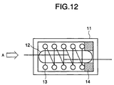
- Fig. 12 illustrates a general construction of a prior art reed switch type shock sensor, shown in JPA No. 8-29444, which is used in an air bag system for automobiles.
- a magnet 14 is housed in a case 11 and held in position by a spring 13.
- a reed switch 12 extends through the spring 13 and is loosely received in the magnet 14.
- the reed switch 12 in the case 11 is open since the magnet 14 is located outside of an area in which the reed switch 12 is responsive to the magnetic field of the magnet 14.
- a shock applied to the shock sensor for example, in a direction shown by an arrow A imposes an acceleration on the mass of the spring 13. If the acceleration is large enough to overcome the resilient force of the spring 13, the magnet 14 moves into the area in which the reed switch 12 is responsive to the magnetic field of the magnet 14 to close its contacts.
- a problem with the prior art reed switch type shock sensor is that the sensor is sensitive to shocks only in the direction shown by arrow A in Fig. 12. Another problem is that the sensitivity of the sensor varies with the weight, dimension, and magnetic flux density of the magnet 14. Further, the use of a reed switch as a shock-detecting element is an obstacle to miniaturizing the shock sensor.
- An object of the invention is to provide a shock sensor which does not incorporate a magnet that suffers from variations in the characteristics such as size, magnetic flux density, and weight and which can detect shocks from almost all directions in a plane.
- a coil (24) produces a magnetic field (M).
- a magnetic fluid (25) is sealed in a closed container located in the magnetic field (M).
- a magnetoresistive effect element (22) is located in the magnetic field (M) and opposes the magnetic fluid (25).
- the magnetic fluid (25) receives a shock, the magnetic fluid (25) moves relative to the magnetoresistive effect element (22) in a direction parallel to a plane in which the magnetoresistive element (22) lies.
- the magnetoresistive effect element (22) is subjected to a change in the magnetic field (M), so that the resistance of the magnetoresistive effect element (22) changes accordingly.
- the magnetoresistive effect element (22) may include four elements (R1-R4) electrically connected in a bridge configuration and the output of the magnetoresistive effect element (22) is processed by an output circuit.
- the output circuit outputs a sensor output in response to an applied shock.
- Fig. 1 illustrates a construction of a shock sensor according to a first embodiment.
- the shock sensor of the first embodiment can be used in place of a prior art reed switch type shock sensor.
- the shock sensor 20 includes a magnetoresistive effect element 22, shaper 23 that reforms the output of the magnetoresistive effect element 22, coil 24 that applies a bias magnetic field M to the magnetoresistive effect element 22, magnetic fluid 25, and container 26 that is closed to seal the magnetic fluid 25, all being accommodated in a case 21.
- a voltage Vcc is applied to the coil 24 so that the coil 24 produces a magnetic field in a direction shown by arrow E.
- the magnetic fluid 25 is attracted to the central area of the magnetic flux produced by the coil 24 and is collected to the middle portion of the container 26 where the magnetic fluid 25 is at its neutral position.
- the neutral position is a position where the magnetic fluid 25 is at rest over the magnetoresistive effect element 22 when no shock is applied thereto.
- the magnetoresistive effect element 22 is a resistor whose electrical resistance varies in accordance with the magnetic field strength in which the magnetoresistive effect element 22 is placed.
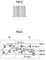
- a magnetoresistive effect element is a thin film of an alloy whose major composition is a ferromagnetic metal and whose pattern is, for example, a meander line as shown in Fig. 3. When a magnetoresistive effect element is magnetized by an external magnetic field, the resistivity of the magnetoresistive effect element varies.
- Fig. 4 is a schematic diagram showing a construction of the shaper 23.
- the magnetoresistive effect element 22 is formed of elements R1-R4 and is placed in the magnetic field generated by the coil 24.
- the elements R1-R4 are connected in a bridge configuration, each element forming one arm of the bridge.
- the junction of R1 and R3 is connected to the supply voltage Vcc and the junction of R2 and R4 is connected to the ground GND.
- Output J is obtained from the junction of R1 and R2 and output K is obtained from the junction of R3 and R4.
- the elements R1-R4 each have an electrical resistance in the range from 2 to 3 K ⁇ .
- the elements R1-R4 must be an MR element and the other elements may be ordinary resistors.
- the elements R1-R4 may be arranged in a plane normal to the direction E of the magnetic field M or in a plane parallel to the direction E of the magnetic field M. Moreover, the elements may also the aligned in the direction E of the magnetic field M in any way as far as the bridge becomes unbalanced when the magnetic fluid 25 displaces with respect to the magnetoresistive effect element 22.
- Figs. 2A-2D illustrate the positional relationships between the elements R1-R4 and the magnetic fluid 25 in the magnetic field M of the coil 24. Shocks applied in directions shown by arrows cause the magnetic fluid 25 to move in the directions shown by arrows so that the bridge circuit becomes unbalanced.
- an operational amplifier A is a differential amplifier
- an operational amplifier B is an inverse-logarithmic amplifier
- an operational amplifier C is a voltage comparator
- the resistors R5 and R6 form a voltage divider to provide a reference voltage Vr.
- the amplifier C outputs a sensor output Vout.
- the output J is fed to an inversion terminal of the operational amplifier A and the output K is input to an inversion terminal.
- the operational amplifier A amplifies the difference between the outputs J and K.
- the output of the operational amplifier A is input to an inversion terminal of the operational amplifier B and the non-inversion terminal of the operational amplifier B is connected to the junction of bias resistors R10 and R11.
- the operational amplifier B performs inverse-logarithmic amplification of the output of the operational amplifier A.
- An inversion terminal of the operational amplifier C receives the output of the operational amplifier B and a non-inversion terminal of the operational amplifier C receives a reference voltage Vr on the junction of the resistors R5 and R6.
- the operational amplifier C compares the output of the operational amplifier B with the reference voltage Vr and outputs an amplified difference between the two inputs thereto, as an output Vout.
- the shock sensor 20 when the shock sensor 20 receives a shock in a direction in a plane including Y and Z axes, the magnetic fluid 25 moves out of its neutral position if the shock is large enough to overcome the magnetic attraction which attracts the magnetic fluid 25. Therefore, the magnetoresistive effect element 22 is subject to changes in magnetic field.
- a change in the magnetic field applied to the magnetoresistive effect element 22 causes changes in the outputs J and K of the bridge circuit of elements R1-R4.
- the operational amplifier A amplifies the difference between the outputs J and K and outputs an output voltage at point a as shown in Fig. 5.
- the output voltage varies in accordance with the acceleration applied to the shock sensor, i.e. the displacement of the magnetic fluid with respect to the magnetoresistive effect element 22.
- the operational amplifier B receives the output of the operational amplifier A and amplifies it inverse-logarithmically.
- Fig. 6 illustrates the output of the operational amplifier B, showing the output which changes linearly with acceleration applied to the shock sensor.
- the output of the operational amplifier B is then input to an inversion input of the operational amplifier C.
- the operational amplifier C compares the input on the inversion input with the reference voltage Vr, and outputs a signal of a logic level "1" if the input from the operational amplifier B is lower than the reference voltage Vr and a signal of a logic level "0" if the input from the operational amplifier B is higher than the reference voltage Vr.
- shock sensor 20 does not use a permanent magnet, characteristics of the sensor are free from any influences of the variations of the weight, dimension, and magnetic flux density of the magnet.
- the senor is not only sensitive to unidirectional shocks, but is capable of detecting shocks from all directions in a plane in which the Y-axis and Z-axis lie.
- the shock sensor of the first embodiment when applied as a sensor to, for example, an air bag system for automobiles, the shock sensor can detect shocks from many directions, increasing reliability of the air bag system.
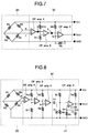
- Fig. 7 illustrates a configuration of a shaper used in a shock sensor of a second embodiment. Elements similar to those in Fig. 4 have been given the same references and description thereof is omitted.
- the shaper includes external resistors which are replaceable or adjustable. Selecting the resistances of the resistors allows setting of a proper operating point of the shock sensor.
- resistors R5 and R6 provide a reference voltage Vr which is supplied to the non-inversion terminal of the operational amplifier C.
- the resistors R5 and R6 have a resistance of about 5 k ⁇ .
- the resistor R6 is a variable resistor or replaceable resistor.
- the resistor R6 may include a plurality of resistors which are selectively used.
- the reference voltage applied to the non-inversion terminal of the operational amplifier C may be set by varying the resistor R6. Varying the resistor R6 allows setting of the threshold point of the sensor at which the shock sensor outputs a sensor output of a logic level "1" or "0” in accordance with the changes in the outputs J and K of the magnetoresistive effect element 22.
- the operating point of the operational amplifier C is set at point R on the curve in Fig. 6.
- the sensor will be activated only when the magnitude of a shock applied to the sensor overcomes an acceleration corresponding to point R.
- the second embodiment is of a construction where the shaper 30 of the magnetoresistive effect element 22 includes a variable or replaceable resistor R6 so that the sensitivity of the shock sensor may be adjusted.
- Fig. 8 is a schematic diagram illustrates a construction of a shaper for use in a shock sensor according to a third embodiment. Elements similar to those in Fig. 4 have been given the same references and description thereof is omitted.
- the third embodiment includes a timer circuit 41 such as a monostable multivibrator incorporated in the shaper.
- the timer 41 outputs an output having a predetermined time length.
- a monostable multivibrator (timer circuit) 41 receives the output of the operational amplifier C of the shaper 40, the multivibrator 41 including an operational amplifier C, capacitors Cp and Ct, diodes D1 and D2, and resistors R T , and R7-R9.
- the resistors R7 and R9 are of the same resistance.
- the operational amplifier A amplifies the output of the magnetoresistive effect element 22 in Fig. 8
- the operational amplifier B inverse-logarithmically amplifies the output of the operational amplifier A.
- the output of the operational amplifier B is directed to the inversion terminal of the operational amplifier C and a reference voltage Vr is applied to the non-inversion terminal.
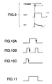
- the operational amplifier C outputs a negative trigger pulse as shown in Fig. 9 via a capacitor Cp to the inversion terminal operational amplifier D. Therefore, the output Vout goes up to +V as shown in Fig. 9.
- the voltage at point Q also increases so that the voltage V RT across the resistor R T increases as shown in Fig. 9.
- the timer outputs the waveform shown in Fig. 11 when triggered by the first negative going edge of any one of the waveforms shown in Figs. 10A-10C. Selecting the values of capacitors and resistors allows adjusting of the height and duration of the waveform shown in Fig. 11.
- the shock sensor according to the third embodiment having a monostable multivibrator 41 is capable of outputting a waveform of a predetermined time duration irrespective of the shape of trigger pulse.
- the shock sensor of the embodiment will increase reliability of an air bag system for use in automobiles.
- the shock sensor of the embodiment is applicable not only to air bag systems for automobiles but also to any apparatuses which need to detect shocks.
- the aforementioned embodiments are not limited to the types of magnetoresistive effect element, magnetic fluid, and Op amps and the number of these parts.
Landscapes
- Physics & Mathematics (AREA)
- General Physics & Mathematics (AREA)
- Measuring Magnetic Variables (AREA)
- Air Bags (AREA)
- Geophysics And Detection Of Objects (AREA)
- Force Measurement Appropriate To Specific Purposes (AREA)
Abstract
Description
Claims (7)
- A shock sensor, comprising:a coil (24), producing a magnetic field;a magnetoresistive effect element (22) placed in the magnetic field produced by said coil (24);a magnetic fluid (25), sealed in a closed container (26) located in the magnetic field and opposing said magnetoresistive effect element (22), said magnetic fluid (25) moving with respect to said magnetoresistive effect element (22) when a shock greater than a predetermined value is applied to said magnetic fluid (25); andan output circuit, processing an output of said magnetoresistive effect element (22) to output a sensor output when said magnetic fluid moves with respect to said magnetoresistive effect element (22) in response to the shock greater than the predetermined value is applied.
- The shock sensor of Claim 1, wherein said output circuit includes a circuit element (R6) for adjusting a characteristic of said output circuit.
- The shock sensor of Claim 2, wherein said characteristic is an operating point (R) of the shock sensor corresponding to a magnitude of a shock for which said output circuit outputs the sensor output
- The shock sensor of Claim 2, wherein said circuit element (R6) is an external resistor which is variable or replaceable.
- The shock sensor of Claim 1, wherein said magnetoresistive effect element (22) includes four elements (R1-R4) aligned at predetermined intervals and electrically connected in a bridge configuration, each element being a predetermined distance away from a central area of the magnetic field.
- The shock sensor of Claim 1, wherein said output circuit includes a circuit (41) which outputs a signal having a predetermined duration (Fig. 11).
- The shock sensor of Claim 6, wherein said timer circuit (41) is a monostable multivibrator.
Applications Claiming Priority (3)
| Application Number | Priority Date | Filing Date | Title |
|---|---|---|---|
| JP322712/96 | 1996-12-03 | ||
| JP8322712A JPH10160748A (en) | 1996-12-03 | 1996-12-03 | Impact sensor |
| JP32271296 | 1996-12-03 |
Publications (2)
| Publication Number | Publication Date |
|---|---|
| EP0848257A1 true EP0848257A1 (en) | 1998-06-17 |
| EP0848257B1 EP0848257B1 (en) | 2003-05-07 |
Family
ID=18146787
Family Applications (1)
| Application Number | Title | Priority Date | Filing Date |
|---|---|---|---|
| EP97121060A Expired - Lifetime EP0848257B1 (en) | 1996-12-03 | 1997-12-01 | Shock or acceleration sensor |
Country Status (6)
| Country | Link |
|---|---|
| US (1) | US5970794A (en) |
| EP (1) | EP0848257B1 (en) |
| JP (1) | JPH10160748A (en) |
| KR (1) | KR100329913B1 (en) |
| CN (1) | CN1186229A (en) |
| DE (1) | DE69721704T2 (en) |
Cited By (1)
| Publication number | Priority date | Publication date | Assignee | Title |
|---|---|---|---|---|
| DE102008003213A1 (en) | 2007-10-15 | 2009-07-09 | Nivag Handelsgesellschaft Mbh | Emergency hammer with additional functions as a shell of a multipurpose tool with signaling |
Families Citing this family (13)
| Publication number | Priority date | Publication date | Assignee | Title |
|---|---|---|---|---|
| US5970744A (en) * | 1998-12-01 | 1999-10-26 | Tiffany And Company | Cut cornered square mixed-cut gemstone |
| US7266988B2 (en) * | 2004-10-15 | 2007-09-11 | Morgan Research Corporation | Resettable latching MEMS shock sensor apparatus and method |
| DE102006010484A1 (en) * | 2006-03-07 | 2007-09-13 | Robert Bosch Gmbh | motion sensor |
| US7401515B2 (en) * | 2006-03-28 | 2008-07-22 | Honeywell International Inc. | Adaptive circuits and methods for reducing vibration or shock induced errors in inertial sensors |
| JP2009537036A (en) * | 2006-05-12 | 2009-10-22 | エヌエックスピー ビー ヴィ | Current interface with blocking capacitor connected to additional pin |
| US8120463B2 (en) * | 2007-01-04 | 2012-02-21 | Lockheed Martin Corporation | RFID protocol for improved tag-reader communications integrity |
| EP1958586A1 (en) * | 2007-02-19 | 2008-08-20 | BrainLAB AG | Surgical device with impact determinator |
| JP5060871B2 (en) * | 2007-08-22 | 2012-10-31 | セイコーインスツル株式会社 | Variable voltage dividing circuit and magnetic sensor circuit |
| TWI365978B (en) * | 2007-12-28 | 2012-06-11 | Ind Tech Res Inst | Method and apparatus for dropping indicator |
| TWI375033B (en) * | 2008-04-09 | 2012-10-21 | Ind Tech Res Inst | All-directional fall sensor and the method thereof |
| CN104977428B (en) * | 2015-07-01 | 2017-12-01 | 泉州市福连天电子科技有限公司 | Vehicle collision inductor full-automatic testing device |
| WO2017127662A1 (en) | 2016-01-22 | 2017-07-27 | Trc Services, Inc. | Automated sucker rod spacing device |
| US11168549B2 (en) | 2016-01-22 | 2021-11-09 | Trc Services, Inc. | Automated sucker rod spacing device and associated methods |
Citations (7)
| Publication number | Priority date | Publication date | Assignee | Title |
|---|---|---|---|---|
| JPS60133370A (en) * | 1983-12-21 | 1985-07-16 | Diesel Kiki Co Ltd | Acceleration sensor |
| US4676103A (en) * | 1985-12-12 | 1987-06-30 | Diesel Kiki Co., Ltd. | Acceleration or inclination sensors |
| EP0293784A2 (en) * | 1987-05-30 | 1988-12-07 | Nippon Soken, Inc. | Acceleration sensor |
| EP0306178A2 (en) * | 1987-08-18 | 1989-03-08 | Fujitsu Limited | Acceleration sensor |
| US4984463A (en) * | 1988-09-28 | 1991-01-15 | Nippon Soken, Inc. | Two-dimensional acceleration sensor |
| EP0419041A1 (en) * | 1989-09-19 | 1991-03-27 | Texas Instruments Incorporated | Speed/position sensor based upon magnetoresistive effect |
| JPH06229788A (en) * | 1993-02-08 | 1994-08-19 | Toyota Autom Loom Works Ltd | Sense of equilibrium sensor |
Family Cites Families (7)
| Publication number | Priority date | Publication date | Assignee | Title |
|---|---|---|---|---|
| US3906802A (en) * | 1972-04-24 | 1975-09-23 | Asahi Chemical Ind | Fluid crash sensor |
| US4631954A (en) * | 1982-11-18 | 1986-12-30 | Mills Manuel D | Apparatus for controlling a pumpjack prime mover |
| JPS63122902A (en) * | 1986-11-13 | 1988-05-26 | Ckd Controls Ltd | Apparatus for confirming position of moving body |
| JPH0277654A (en) * | 1988-09-14 | 1990-03-16 | Nippon Seiko Kk | Impact sensor |
| US5610817A (en) * | 1993-02-08 | 1997-03-11 | Breed Automotive Technology, Inc. | Passenger restraint system with an electronic crash sensor |
| JP2658855B2 (en) * | 1993-12-28 | 1997-09-30 | 日本電気株式会社 | Shock sensing device |
| JPH0829444A (en) * | 1994-07-19 | 1996-02-02 | Oki Electric Ind Co Ltd | Impact sensor |
-
1996
- 1996-12-03 JP JP8322712A patent/JPH10160748A/en not_active Withdrawn
-
1997
- 1997-12-01 EP EP97121060A patent/EP0848257B1/en not_active Expired - Lifetime
- 1997-12-01 KR KR1019970065074A patent/KR100329913B1/en not_active IP Right Cessation
- 1997-12-01 DE DE69721704T patent/DE69721704T2/en not_active Expired - Fee Related
- 1997-12-02 CN CN97123065A patent/CN1186229A/en active Pending
- 1997-12-03 US US08/984,683 patent/US5970794A/en not_active Expired - Lifetime
Patent Citations (7)
| Publication number | Priority date | Publication date | Assignee | Title |
|---|---|---|---|---|
| JPS60133370A (en) * | 1983-12-21 | 1985-07-16 | Diesel Kiki Co Ltd | Acceleration sensor |
| US4676103A (en) * | 1985-12-12 | 1987-06-30 | Diesel Kiki Co., Ltd. | Acceleration or inclination sensors |
| EP0293784A2 (en) * | 1987-05-30 | 1988-12-07 | Nippon Soken, Inc. | Acceleration sensor |
| EP0306178A2 (en) * | 1987-08-18 | 1989-03-08 | Fujitsu Limited | Acceleration sensor |
| US4984463A (en) * | 1988-09-28 | 1991-01-15 | Nippon Soken, Inc. | Two-dimensional acceleration sensor |
| EP0419041A1 (en) * | 1989-09-19 | 1991-03-27 | Texas Instruments Incorporated | Speed/position sensor based upon magnetoresistive effect |
| JPH06229788A (en) * | 1993-02-08 | 1994-08-19 | Toyota Autom Loom Works Ltd | Sense of equilibrium sensor |
Non-Patent Citations (2)
| Title |
|---|
| PATENT ABSTRACTS OF JAPAN vol. 009, no. 296 (P - 407) 22 November 1985 (1985-11-22) * |
| PATENT ABSTRACTS OF JAPAN vol. 018, no. 609 (P - 1828) 18 November 1994 (1994-11-18) * |
Cited By (1)
| Publication number | Priority date | Publication date | Assignee | Title |
|---|---|---|---|---|
| DE102008003213A1 (en) | 2007-10-15 | 2009-07-09 | Nivag Handelsgesellschaft Mbh | Emergency hammer with additional functions as a shell of a multipurpose tool with signaling |
Also Published As
| Publication number | Publication date |
|---|---|
| EP0848257B1 (en) | 2003-05-07 |
| KR19980063663A (en) | 1998-10-07 |
| DE69721704D1 (en) | 2003-06-12 |
| US5970794A (en) | 1999-10-26 |
| CN1186229A (en) | 1998-07-01 |
| KR100329913B1 (en) | 2002-09-19 |
| JPH10160748A (en) | 1998-06-19 |
| DE69721704T2 (en) | 2004-03-25 |
Similar Documents
| Publication | Publication Date | Title |
|---|---|---|
| US5970794A (en) | Shock sensor | |
| US5983724A (en) | Shock sensor with rotating magnetorestrictive effect element | |
| AU600412B2 (en) | Magnetically-damped testable accelerometer | |
| US5177370A (en) | Impact sensor for vehicle safety restraint system | |
| EP2966453A1 (en) | MLU based accelerometer using a magnetic tunnel junction | |
| WO2006035371A1 (en) | Sensor arrangement | |
| GB2191863A (en) | Improvements in motion sensors | |
| US3861488A (en) | Collision speed sensor | |
| US6184764B1 (en) | Pendulum mass acceleration sensor | |
| JPS634980B2 (en) | ||
| EP1817548B1 (en) | Adaptive geartooth sensor with dual peak detectors and true power on capability | |
| EP1150125A1 (en) | Charge-type sensor amplifying circuit | |
| US6850136B2 (en) | Magnetoresistive based electronic switch | |
| JPH08335253A (en) | Detecting circuit for insertion and ejection of magnetic card into and from magnetic card reader | |
| US4994741A (en) | Magnetic motion sensing device for sensing inclination and swaying | |
| JPH02189484A (en) | Magnetic sensor | |
| JP2658855B2 (en) | Shock sensing device | |
| JPH0634711Y2 (en) | Magnetic sensor | |
| US3665769A (en) | Acceleration switch | |
| JP2684062B2 (en) | Sensor abnormality detection circuit | |
| JPH0829444A (en) | Impact sensor | |
| JPH081387B2 (en) | Magnetic sensor | |
| JPH04271425A (en) | Contactless position detector | |
| Canteli | Sensors | |
| SEMICONDUCTORS | Magnetic field sensor |
Legal Events
| Date | Code | Title | Description |
|---|---|---|---|
| PUAI | Public reference made under article 153(3) epc to a published international application that has entered the european phase |
Free format text: ORIGINAL CODE: 0009012 |
|
| AK | Designated contracting states |
Kind code of ref document: A1 Designated state(s): DE FR IT |
|
| AX | Request for extension of the european patent |
Free format text: AL;LT;LV;MK;RO;SI |
|
| 17P | Request for examination filed |
Effective date: 19981030 |
|
| AKX | Designation fees paid |
Free format text: DE FR IT |
|
| RBV | Designated contracting states (corrected) |
Designated state(s): DE FR IT |
|
| 17Q | First examination report despatched |
Effective date: 20000403 |
|
| GRAH | Despatch of communication of intention to grant a patent |
Free format text: ORIGINAL CODE: EPIDOS IGRA |
|
| GRAH | Despatch of communication of intention to grant a patent |
Free format text: ORIGINAL CODE: EPIDOS IGRA |
|
| GRAH | Despatch of communication of intention to grant a patent |
Free format text: ORIGINAL CODE: EPIDOS IGRA |
|
| GRAA | (expected) grant |
Free format text: ORIGINAL CODE: 0009210 |
|
| AK | Designated contracting states |
Designated state(s): DE FR IT |
|
| REF | Corresponds to: |
Ref document number: 69721704 Country of ref document: DE Date of ref document: 20030612 Kind code of ref document: P |
|
| ET | Fr: translation filed | ||
| PGFP | Annual fee paid to national office [announced via postgrant information from national office to epo] |
Ref country code: FR Payment date: 20031218 Year of fee payment: 7 |
|
| PGFP | Annual fee paid to national office [announced via postgrant information from national office to epo] |
Ref country code: DE Payment date: 20040301 Year of fee payment: 7 |
|
| PLBE | No opposition filed within time limit |
Free format text: ORIGINAL CODE: 0009261 |
|
| STAA | Information on the status of an ep patent application or granted ep patent |
Free format text: STATUS: NO OPPOSITION FILED WITHIN TIME LIMIT |
|
| 26N | No opposition filed |
Effective date: 20040210 |
|
| PG25 | Lapsed in a contracting state [announced via postgrant information from national office to epo] |
Ref country code: DE Free format text: LAPSE BECAUSE OF NON-PAYMENT OF DUE FEES Effective date: 20050701 |
|
| PG25 | Lapsed in a contracting state [announced via postgrant information from national office to epo] |
Ref country code: FR Free format text: LAPSE BECAUSE OF NON-PAYMENT OF DUE FEES Effective date: 20050831 |
|
| REG | Reference to a national code |
Ref country code: FR Ref legal event code: ST |
|
| PG25 | Lapsed in a contracting state [announced via postgrant information from national office to epo] |
Ref country code: IT Free format text: LAPSE BECAUSE OF NON-PAYMENT OF DUE FEES Effective date: 20051201 |