EP0844600B1 - Power-saving mode for a liquid crystal device with two display portions - Google Patents
Power-saving mode for a liquid crystal device with two display portions Download PDFInfo
- Publication number
- EP0844600B1 EP0844600B1 EP97309339A EP97309339A EP0844600B1 EP 0844600 B1 EP0844600 B1 EP 0844600B1 EP 97309339 A EP97309339 A EP 97309339A EP 97309339 A EP97309339 A EP 97309339A EP 0844600 B1 EP0844600 B1 EP 0844600B1
- Authority
- EP
- European Patent Office
- Prior art keywords
- liquid crystal
- crystal display
- voltage
- electrodes
- operation mode
- Prior art date
- Legal status (The legal status is an assumption and is not a legal conclusion. Google has not performed a legal analysis and makes no representation as to the accuracy of the status listed.)
- Expired - Lifetime
Links
Images


Classifications
-
- G—PHYSICS
- G09—EDUCATION; CRYPTOGRAPHY; DISPLAY; ADVERTISING; SEALS
- G09G—ARRANGEMENTS OR CIRCUITS FOR CONTROL OF INDICATING DEVICES USING STATIC MEANS TO PRESENT VARIABLE INFORMATION
- G09G3/00—Control arrangements or circuits, of interest only in connection with visual indicators other than cathode-ray tubes
- G09G3/20—Control arrangements or circuits, of interest only in connection with visual indicators other than cathode-ray tubes for presentation of an assembly of a number of characters, e.g. a page, by composing the assembly by combination of individual elements arranged in a matrix no fixed position being assigned to or needed to be assigned to the individual characters or partial characters
- G09G3/34—Control arrangements or circuits, of interest only in connection with visual indicators other than cathode-ray tubes for presentation of an assembly of a number of characters, e.g. a page, by composing the assembly by combination of individual elements arranged in a matrix no fixed position being assigned to or needed to be assigned to the individual characters or partial characters by control of light from an independent source
- G09G3/36—Control arrangements or circuits, of interest only in connection with visual indicators other than cathode-ray tubes for presentation of an assembly of a number of characters, e.g. a page, by composing the assembly by combination of individual elements arranged in a matrix no fixed position being assigned to or needed to be assigned to the individual characters or partial characters by control of light from an independent source using liquid crystals
- G09G3/3611—Control of matrices with row and column drivers
-
- G—PHYSICS
- G09—EDUCATION; CRYPTOGRAPHY; DISPLAY; ADVERTISING; SEALS
- G09G—ARRANGEMENTS OR CIRCUITS FOR CONTROL OF INDICATING DEVICES USING STATIC MEANS TO PRESENT VARIABLE INFORMATION
- G09G2330/00—Aspects of power supply; Aspects of display protection and defect management
- G09G2330/02—Details of power systems and of start or stop of display operation
- G09G2330/021—Power management, e.g. power saving
Definitions
- the present invention relates to a liquid crystal device for example of the type used in an apparatus in which a battery is the main power source, such as a portable telephone and a pager.
- Fig. 2 is a block diagram illustrating the structure of a general liquid crystal display device.
- Power source voltage 7 is boosted, normally to be doubled or tripled, by a booster circuit 9 provided within an IC 8.
- a voltage regulator circuit 10 After the voltage is regulated, for driving the liquid crystal, by a voltage regulator circuit 10; a bias voltage for driving the liquid crystal panel is generated by a bias voltage generator circuit 11. Further, the generated bias voltage is connected, via a voltage stabiliser circuit 12 for stabilising the voltage, to a scan electrode drive circuit 13 and to a signal electrode driver circuit 14. Ultimately the voltage is applied to a scan electrode terminal and a signal electrode terminal of the liquid crystal panel 15.
- a scan electrode group 16 forming a dot matrix portion and a scan electrode 17 forming an icon portion face a signal electrode group 18.
- all pixels of the dot matrix portion and the icon portion formed as the intersections of the scan electrode group 16, the scan electrode 17 and the signal electrode group 18 can be made to be in an arbitrary state of display in the same duty ratio.
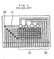
- a scan electrode and its corresponding signal electrode group 20 forming an icon portion are separately provided so as to face each other.
- the dot matrix portion and the icon portion can be made to be in arbitrary states of display in independent duty ratios.
- a selected waveform is applied line-sequentially to each of the scan electrodes. After the selected waveform is applied to every scan electrodes, scanning is repeated again in the same way.
- the time necessary for one cycle of such a scan is referred to as the frame period, and its frequency is referred to as the frame frequency.
- the ratio of selection time of each of the scan electrode (time necessary for applying a selected waveform to the scan electrode) to the frame period is referred to as the duty ratio.
- the time shared drive method an electric field is applied not only to ON (selected) pixels but also to OFF (unselected) pixels. Therefore, it is necessary for the electro-optical characteristic of the LCD to have an appropriate response threshold.
- a waveform for controlling the state of display is applied only for a predetermined length of time which depends on the duty ratio, and a waveform unrelated to the control of the state of display is applied for the remaining, majority of the time. Since the liquid crystal also responds to the waveform applied in this non-selection time, it is necessary to control carefully the effective voltage of the waveform applied in the non-selection time.
- This driving method is referred to as the voltage averaging method, and this is adopted by all time shared drive LCDs now put to practical use.
- Fig. 5 shows examples of waveforms of the voltage averaging method under a general condition where the duty ratio is 1/N and the bias is 1/a.
- Figs. 5A and 5B show waveforms applied to a first scan electrode and a second scan electrode, respectively.
- Fig. 5C shows a waveform applied to signal electrodes in case of all pixels being the in display (selected) state.
- Fig. 5D shows a waveform applied to the signal electrodes in the case of all pixels being in the non-display (unselected) state.
- Fig. 5E shows a waveform applied to an individual selected pixel.
- Fig. 5F shows a waveform applied to an individual unselected pixel.
- EP 0474231A describes a display device in which an image for display can be displayed on the whole of the display screen or on one quarter of the screen. In order to reduce power consumption only selected display drivers are used in the quarter screen mode.
- EP 0651367A describes a liquid crystal display in which power consumption can be reduced by determining whether the image signals of the next field to be displayed are those for a fixed image display or a moving image display. If a fixed image is to be displayed, either a spread-out mode or a low voltage mode is initiated to reduce power consumption.
- an object of the present invention is to provide a liquid crystal display device having a small area of a substrate forming the liquid crystal device and which at the same time can cut down power consumption.
- the area necessary for the wiring of the signal electrode group need not be enlarged.
- the duty ratio can be smaller in the power-saving operation mode, compared with a conventional liquid crystal display device driven with the same frame frequency, in the present invention the operation clock of the circuit for producing the drive waveform can be delayed or the operation of the circuit can be stopped. Thus, power consumption can be reduced.
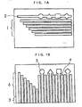
- FIGs. 1A and 1B are schematic views illustrating wirings of a scan electrode group and a signal electrode group of a liquid crystal panel for use in a comparative example and an embodiment of the present invention.
- a scan electrode group 1 forming a dot matrix portion on a substrate is formed in the shape of stripes, and a scan electrode 2 forming an icon portion is formed opposite to an electrode terminal group 3 formed on the opposing substrate of the LCD panel.
- a signal electrode group 4 forming only a dot matrix portion on the other substrate is in the shape of stripes, and signal electrodes 5 forming both the dot portion and the icon portion are formed at the ends of the lines so as to have a shape matching the icons.
- Wirings 6 are formed on the substrate carrying the signal electrodes so that electrode terminals for the scan electrodes are formed thereon.
- a power source voltage of 3V is boosted so as to be doubled to 6V by a booster circuit integrated within the IC.
- a waveform for driving the liquid crystal is generated via a bias voltage generator circuit and a voltage stabiliser circuit.
- the duty ratio is 1/33
- the bias is 1/6
- the voltage regulator circuit produces a voltage for driving the liquid crystal of 5.8V.
- the voltage regulator circuit produces a voltage of 3.0V for driving the liquid crystal.
- the signal electrodes for the icons are regarded as a first scan electrode.
- the whole of the signal electrodes for the dot matrix are regarded as second scan electrodes.
- the electrodes are driven with a duty ratio of 1/2 and with a bias of 1/2. Waveforms for driving were in accordance with the normal voltage averaging method.
- the duty ratio is 1/33 and the bias 1/6 in the normal mode and in the power-save mode the duty is 1/2 and the bias is 1/2, it will be readily apparent that a similar effect can be obtained by other kinds of combination.
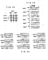
- Fig. 6 shows an embodiment of the drive waveforms according to the present invention.
- a display pixel portion is formed by an upper icon scan electrode com-1, a lower icon scan electrode com-3, dot matrix scan electrodes com-2 [with a scan electrode group 1 forming the dot matrix portion generally referred to as the dot matrix scan electrodes com-2] and signal electrodes seg-1, 2, and 3.
- the figure shows the case where the pixels formed by seg-1 and com-1 and by seg-3 and com-3 are selected and the other pixels are unselected. Waveforms applied to the respective scan electrodes and the respective signal electrodes in this case are shown in Fig. 6B.
- Fig. 6C shows waveforms applied between the scan electrodes and the signal electrodes, that is applied to the respective display pixels.
- Fig. 6 shows an example where alternation occurs in a two-frame cycle
- the present invention is not limited thereto.
- Fig. 7 shows drive waveforms in a power-saving operation mode and an embodiment of a driving method according to the present invention. Similar to Fig. 6, Fig. 7A shows a display pixel portion formed by icon scan electrodes com-1 and com-3, dot matrix scan electrodes com-2, and signal electrodes seg-1, 2, and 3. Pixels shown as ⁇ are selected while pixels shown as O are unselected.
- Waveforms applied to the respective scan electrodes and the respective signal electrodes in this case are shown in Fig. 7B. Further, Fig. 7C shows waveforms applied between the scan electrodes and the signal electrodes; that is, to the respective display pixels.
- the effective voltage applied to the liquid crystal panel can be regulated.
- Table 1 shows the effective voltage when the waveforms are applied to the selected pixels and to the unselected pixels, respectively.
- the selection time of the scan electrodes is 1 and the value of the electric potential A is varied from 1 to 10. It is to be noted that the drive voltage is, similar to the above, 3.0 V.
- the power source voltage can be used without boosting and without voltage regulation; the use of a booster circuit, voltage regulator circuit, bias voltage generator circuit and voltage stabiliser circuit can be avoided.
- the electric current in the normal operation mode in the embodiment was 90 ⁇ A
- the electric current in the power-saving operation mode where such waveforms were applied and only the icons were displayed was 10 ⁇ A.
- a liquid crystal display device which can greatly cut down power consumption in a power-saving operation mode where only icons are displayed, without enlarging the area necessary for the wiring of the signal electrode group.
- the operating mode is changed to the power save mode when the display device is in standby mode or generally waiting for operation.
- the invention is not dependent upon the use of electrodes configured as shown in Figures 1A and 1B.
- a description has been given in terms of a dot matrix display portion and an icon display portion but the invention is not limited thereto.
- the icon display portion may instead be a digit display portion or a segment display portion.
Description
- The present invention relates to a liquid crystal device for example of the type used in an apparatus in which a battery is the main power source, such as a portable telephone and a pager.
- First, the structure of a conventional liquid crystal display device will be described with reference to Fig. 2 which is a block diagram illustrating the structure of a general liquid crystal display device.
Power source voltage 7 is boosted, normally to be doubled or tripled, by abooster circuit 9 provided within anIC 8. After the voltage is regulated, for driving the liquid crystal, by avoltage regulator circuit 10; a bias voltage for driving the liquid crystal panel is generated by a biasvoltage generator circuit 11. Further, the generated bias voltage is connected, via a voltage stabiliser circuit 12 for stabilising the voltage, to a scanelectrode drive circuit 13 and to a signalelectrode driver circuit 14. Ultimately the voltage is applied to a scan electrode terminal and a signal electrode terminal of theliquid crystal panel 15. - Next, a description will be given of the wiring and driving method for the scan electrodes and signal electrodes of a liquid crystal panel used in a conventional liquid crystal display device.
- In a first example, as shown in Fig. 3, a
scan electrode group 16 forming a dot matrix portion and ascan electrode 17 forming an icon portion face asignal electrode group 18. In a liquid crystal panel thus formed, all pixels of the dot matrix portion and the icon portion formed as the intersections of thescan electrode group 16, thescan electrode 17 and thesignal electrode group 18 can be made to be in an arbitrary state of display in the same duty ratio. - Alternatively, and as a second example, in order to independently control the display of the icon portion, as shown in Fig. 4, in addition to a scan electrode group and its corresponding
signal electrode group 19 forming a dot matrix portion, a scan electrode and its correspondingsignal electrode group 20 forming an icon portion are separately provided so as to face each other. In this case, with the dedicatedsignal electrode group 20 for the icons, the dot matrix portion and the icon portion can be made to be in arbitrary states of display in independent duty ratios. - It is to be noted that in Figs. 3 and 4, in order to take out the scan electrode group and the signal electrode group to
electrode terminals 21 on the same substrate, they are connected using an upper/lower conductor 22. - Next, a brief description will be given with regard to the time shared drive method.
- In time shared drive, a selected waveform is applied line-sequentially to each of the scan electrodes. After the selected waveform is applied to every scan electrodes, scanning is repeated again in the same way. The time necessary for one cycle of such a scan is referred to as the frame period, and its frequency is referred to as the frame frequency. The ratio of selection time of each of the scan electrode (time necessary for applying a selected waveform to the scan electrode) to the frame period is referred to as the duty ratio.
- In the time shared drive method, an electric field is applied not only to ON (selected) pixels but also to OFF (unselected) pixels. Therefore, it is necessary for the electro-optical characteristic of the LCD to have an appropriate response threshold. In the time shared drive method, a waveform for controlling the state of display is applied only for a predetermined length of time which depends on the duty ratio, and a waveform unrelated to the control of the state of display is applied for the remaining, majority of the time. Since the liquid crystal also responds to the waveform applied in this non-selection time, it is necessary to control carefully the effective voltage of the waveform applied in the non-selection time.
- The reason for this is to keep uniform the difference in display state between ON pixels and OFF pixels. This driving method is referred to as the voltage averaging method, and this is adopted by all time shared drive LCDs now put to practical use.
- Fig. 5 shows examples of waveforms of the voltage averaging method under a general condition where the duty ratio is 1/N and the bias is 1/a. Figs. 5A and 5B show waveforms applied to a first scan electrode and a second scan electrode, respectively. Fig. 5C shows a waveform applied to signal electrodes in case of all pixels being the in display (selected) state. Fig. 5D shows a waveform applied to the signal electrodes in the case of all pixels being in the non-display (unselected) state. Fig. 5E shows a waveform applied to an individual selected pixel. Fig. 5F shows a waveform applied to an individual unselected pixel.
- Even in the case of the above-mentioned first example, it is possible to make only the icon portion displayed. That is, to make only the icon portion in an arbitrary state of display with the whole dot matrix portion undisplayed. However, in this case, although apparently only the icon portion is displayed, a drive waveform which is the same as in a normal operation mode is applied to all the scan electrodes and all the signal electrode. Thus, no power-saving effect can be obtained.
- In the case of the second example, in order to make the icon portion in an arbitrary state of display with the whole dot matrix portion undisplayed, it is enough to apply a drive waveform only to a dedicated scan electrode and a dedicated signal electrode group for the icons. It is not necessary to apply a drive waveform to the dot matrix portion. As a result, a great power-saving effect can be obtained.
- However, as is clear from Fig. 4, as the number of the icons increases, the number of the dedicated signal electrodes for the icons increases accordingly, and a large area is necessary for the associated wiring.
- US 4764766 A describes a liquid crystal display device according to the preamble of the attached
claim 1. - EP 0474231A describes a display device in which an image for display can be displayed on the whole of the display screen or on one quarter of the screen. In order to reduce power consumption only selected display drivers are used in the quarter screen mode.
- EP 0651367A describes a liquid crystal display in which power consumption can be reduced by determining whether the image signals of the next field to be displayed are those for a fixed image display or a moving image display. If a fixed image is to be displayed, either a spread-out mode or a low voltage mode is initiated to reduce power consumption.
- The present invention seeks to mitigate the problems mentioned above. More specifically, an object of the present invention is to provide a liquid crystal display device having a small area of a substrate forming the liquid crystal device and which at the same time can cut down power consumption.
- In order to solve the above problems, according to the present invention there is provided a liquid crystal display device according to
claim 1. - An embodiment is provided in
claim 2. - In a liquid crystal display device according to the present invention, and as is clear from the embodiment of Fig. 1, the area necessary for the wiring of the signal electrode group need not be enlarged. In addition, since the duty ratio can be smaller in the power-saving operation mode, compared with a conventional liquid crystal display device driven with the same frame frequency, in the present invention the operation clock of the circuit for producing the drive waveform can be delayed or the operation of the circuit can be stopped. Thus, power consumption can be reduced.
- Embodiments of the present invention will now be further described by way of example only and with reference to the accompanying drawings, in which:
- Fig. 1A is a schematic view illustrating wiring of a scan electrode group of a liquid crystal panel for use in an embodiment of the present invention;
- Fig. 1B is a schematic view illustrating wiring of a signal electrode group of the liquid crystal panel for use in an embodiment of the present invention;
- Fig. 2 is a block diagram illustrating the structure of a general liquid crystal display device;
- Fig. 3 is a schematic view illustrating the wiring of a scan electrode group and of a signal electrode group of a conventional liquid crystal panel;
- Fig. 4 is a schematic view illustrating the wiring of a scan electrode group and of a signal electrode group of another conventional liquid crystal panel;
- Fig. 5A is a waveform illustration for explaining a driving method of a conventional liquid crystal display device and shows an example of a waveform applied to a first scan electrode;
- Fig. 5B is a waveform illustration for explaining the driving method of the conventional liquid crystal display device and shows an example of a waveform applied to a second scan electrode;
- Fig. 5C is a waveform illustration for explaining the driving method of the conventional liquid crystal display device and shows an example of a waveform applied to the signal electrodes in case of all of the pixels being selected.
- Fig. 5D is a waveform illustration for explaining the driving method of the conventional liquid crystal display device and shows an example of a waveform applied to the signal electrodes in case of all of the pixels being unselected.
- Fig. 5E is a waveform illustration for explaining the driving method of the conventional liquid crystal display device and shows an example of a waveform applied to a selected (displaying) pixel;
- Fig. 5F is a waveform illustration for explaining the driving method of the conventional liquid crystal display device and shows an example of a waveform applied to an unselected (non-displaying) pixel;
- Fig. 6A is a explanatory drawing for explaining a driving method of a liquid crystal display device according to an embodiment of the present invention and is an explanatory view schematically illustrating scan electrodes and signal electrodes forming pixels;
- Fig. 6B is a waveform illustration for explaining a driving method of the liquid crystal display device according to an embodiment of the present invention and shows an example of waveforms applied to the respective scan electrodes and the respective signal electrodes;
- Fig. 6C is a waveform illustration for explaining a driving method of the liquid crystal display device according to an embodiment of the present invention and shows an example of waveforms applied to the pixels formed by the respective scan electrodes and the respective signal electrodes;
- Fig. 7A is an explanatory drawing for explaining another driving method of the liquid crystal display device according to an embodiment of the present invention and is an explanatory view schematically illustrating the scan electrodes and signal electrodes forming the pixels;
- Fig. 7B is a waveform illustration for explaining a driving method of the liquid crystal display device according to an embodiment of the present invention and shows an example of waveforms applied to the respective scan electrodes and the respective signal electrodes; and
- Fig. 7C shows waveform illustrations for explaining a driving method of the liquid crystal display device according to an embodiment of the present invention and shows an example of waveforms applied to the pixels formed by the respective scan electrodes and the respective signal electrodes.
- Comparative examples and preferred embodiments of the present invention will now be described in more detail. Figs. 1A and 1B are schematic views illustrating wirings of a scan electrode group and a signal electrode group of a liquid crystal panel for use in a comparative example and an embodiment of the present invention. A
scan electrode group 1 forming a dot matrix portion on a substrate is formed in the shape of stripes, and ascan electrode 2 forming an icon portion is formed opposite to anelectrode terminal group 3 formed on the opposing substrate of the LCD panel. Similarly, asignal electrode group 4 forming only a dot matrix portion on the other substrate is in the shape of stripes, andsignal electrodes 5 forming both the dot portion and the icon portion are formed at the ends of the lines so as to have a shape matching the icons.Wirings 6 are formed on the substrate carrying the signal electrodes so that electrode terminals for the scan electrodes are formed thereon. - In a first comparative example, with a liquid crystal display device having the liquid crystal panel structure as shown in Fig. 1; a power source voltage of 3V is boosted so as to be doubled to 6V by a booster circuit integrated within the IC. After the voltage for driving the liquid crystal is generated, by a voltage regulator circuit from the boosted voltage, a waveform for driving the liquid crystal is generated via a bias voltage generator circuit and a voltage stabiliser circuit. In a normal operation mode, the duty ratio is 1/33, the bias is 1/6, and the voltage regulator circuit produces a voltage for driving the liquid crystal of 5.8V. In a power-saving operation mode, the voltage regulator circuit produces a voltage of 3.0V for driving the liquid crystal. The signal electrodes for the icons are regarded as a first scan electrode. The whole of the signal electrodes for the dot matrix are regarded as second scan electrodes. The electrodes are driven with a duty ratio of 1/2 and with a bias of 1/2. Waveforms for driving were in accordance with the normal voltage averaging method.
- As a result, while the electric current in the normal operation mode was 100 µA, the electric current in the power-saving operation mode, where only the icons were displayed thus permitting a delay in the operation clock of the circuit, was 60 µA.
- It is to be noted that, although in the present example the duty ratio is 1/33 and the
bias 1/6 in the normal mode and in the power-save mode the duty is 1/2 and the bias is 1/2, it will be readily apparent that a similar effect can be obtained by other kinds of combination. The higher the duty ratio in the normal operation mode, the higher the drop rate of the power consumption in the power-saving operation mode. - In a second comparative example, with the liquid crystal display device having the liquid crystal panel structure as shown in Fig. 1; in a normal operation mode, similarly to the first example, using a power source voltage of 3V and the above-mentioned circuits within the IC, normal drive is carried out according to the voltage averaging method with the drive voltage being 5.8V, the duty ratio being 1/33 and the bias being 1/6. In a power-saving operation mode, the power source voltage of 3V is used without change and the liquid crystal is driven with a duty ratio of 1/2 and with a bias of 1/2.
- As a result, while the electric current in the normal operation mode was 100 µA, the electric current in the power-saving operation mode where only the icons were displayed was, due to the absence of the booster circuit and the voltage regulator circuit, reduced to 50 µA.
- It will be readily apparent that a similar effect can be obtained by other kinds of combination of the drive conditions of the second comparative example.
- In a first embodiment, with the liquid crystal display device having the liquid crystal panel structure as shown in Fig. 1; in a normal operation mode, similarly to the first example, using a power source voltage of 3V and the above-mentioned circuits within the IC; normal drive was carried out according to the voltage averaging method with the drive voltage being 5.8V, the duty ratio being 1/17 and the bias being 1/4. In contrast, in a power-saving operation mode, a time shared drive waveform of the drive voltage of 3.0V which does not require intermediate voltage (bias voltage) was applied.
- Fig. 6 shows an embodiment of the drive waveforms according to the present invention. As shown in Fig. 6A, a display pixel portion is formed by an upper icon scan electrode com-1, a lower icon scan electrode com-3, dot matrix scan electrodes com-2 [with a
scan electrode group 1 forming the dot matrix portion generally referred to as the dot matrix scan electrodes com-2] and signal electrodes seg-1, 2, and 3. The figure shows the case where the pixels formed by seg-1 and com-1 and by seg-3 and com-3 are selected and the other pixels are unselected. Waveforms applied to the respective scan electrodes and the respective signal electrodes in this case are shown in Fig. 6B. Further, Fig. 6C shows waveforms applied between the scan electrodes and the signal electrodes, that is applied to the respective display pixels. - In a time share drive waveform of this kind where the power source voltage can be used without boosting and without voltage regulation; use of the conventionally required booster circuit, voltage regulator circuit, bias voltage generator circuit, and voltage stabiliser circuit can be avoided. As a result, while the electric current in the normal operation mode in this embodiment was 90 µA, the electric current in the power-saving operation mode where such waveforms were applied and only the icons were displayed was 10 µA.
- It is readily apparent that, though Fig. 6 shows an example where alternation occurs in a two-frame cycle, the present invention is not limited thereto.
- In a second embodiment, with the liquid crystal display device having the liquid crystal panel structure as shown in Fig. 1; in a normal operation mode, similarly to the first embodiment, normal drive was carried out according to the voltage averaging method with the duty ratio being 1/17, the bias being 1/4 and the drive voltage being 4.2V. Fig. 7 shows drive waveforms in a power-saving operation mode and an embodiment of a driving method according to the present invention. Similar to Fig. 6, Fig. 7A shows a display pixel portion formed by icon scan electrodes com-1 and com-3, dot matrix scan electrodes com-2, and signal electrodes seg-1, 2, and 3. Pixels shown as ● are selected while pixels shown as O are unselected. Waveforms applied to the respective scan electrodes and the respective signal electrodes in this case are shown in Fig. 7B. Further, Fig. 7C shows waveforms applied between the scan electrodes and the signal electrodes; that is, to the respective display pixels. By varying the length of time of the electric potential A, shown in the figure, during which the effective voltage can be regulated, the effective voltage applied to the liquid crystal panel can be regulated.
- The following Table 1 shows the effective voltage when the waveforms are applied to the selected pixels and to the unselected pixels, respectively. The selection time of the scan electrodes is 1 and the value of the electric potential A is varied from 1 to 10. It is to be noted that the drive voltage is, similar to the above, 3.0 V.
[Table 1] Value of A Voltage of Selected Pixel [Vrms] Voltage of Unselected Pixel [Vrms} 0 3.000 1.732 1 2.598 1.500 2 2.324 1.342 3 2.121 1.225 4 1.964 1.134 5 1.837 1.061 6 1.732 1.000 7 1.643 0.949 8 1.567 0.905 9 1.500 0.866 10 1.441 0.832 - This permits accommodation to a liquid crystal to which a low voltage is applied.
- Similar to the first embodiment, since the power source voltage can be used without boosting and without voltage regulation; the use of a booster circuit, voltage regulator circuit, bias voltage generator circuit and voltage stabiliser circuit can be avoided. As a result, while the electric current in the normal operation mode in the embodiment was 90 µA, the electric current in the power-saving operation mode where such waveforms were applied and only the icons were displayed was 10 µA.
- It will be readily apparent that, though, in Fig. 7, the electric potential A where the effective voltage is regulated is located at one particular place in one frame, the present invention is not limited thereto.
- As described above, according to the present invention, a liquid crystal display device is provided which can greatly cut down power consumption in a power-saving operation mode where only icons are displayed, without enlarging the area necessary for the wiring of the signal electrode group.
- Generally, it should be understood that the operating mode is changed to the power save mode when the display device is in standby mode or generally waiting for operation. Further, it should be understood that the invention is not dependent upon the use of electrodes configured as shown in Figures 1A and 1B. Moreover, a description has been given in terms of a dot matrix display portion and an icon display portion but the invention is not limited thereto. For example, the icon display portion may instead be a digit display portion or a segment display portion.
Claims (2)
- A liquid crystal display device comprising :a liquid crystal display panel including a first substrate and a second substrate ; a plurality of scanning electrodes (1) formed on the first substrate and associated with a first, dot-matrix display portion; at least one scanning electrode (2) formed the first substrate and associated with a second display portion which is one of an icon display portion, a digit display portion and a segment display portion; a plurality of signal electrodes (4) formed on the second substrate, and a driving circuit for driving the liquid crystal display panel;
characterized in that : the driving circuit is arranged to drive the liquid crystal display pared in a normal operation mode, in which a boosted voltage is supplied to drive the liquid crystal display panel and information is displayed on the first and second display portions, and in a power-save operation mode, in which a non-boosted voltage is supplied to drive the liquid crystal display panel and information is displayed on only the second display portion;the driving circuit is arranged to generate driving waveforms having two voltage levels and to apply the driving waveforms to the plurality of scanning electrodes (1), to the at least one scan electrode (2) and to the plurality of signal electrodes (4) in said power-save operation mode wherein the two voltage levels are a ground voltage level and the voltage level (Vop) for operating the driving-signal generating circuit; andthe plurality of scanning electrodes (1) are driven simultaneously with the same two-level waveform. - A liquid crystal display device according to claim 1, wherein the driving waveforms further comprise a variable length of time over which the ground voltage level is applied, thereby to regulate the effective voltage applied to a liquid crystal layer of the liquid crystal display panel.
Applications Claiming Priority (4)
| Application Number | Priority Date | Filing Date | Title |
|---|---|---|---|
| JP311065/96 | 1996-11-21 | ||
| JP31106596 | 1996-11-21 | ||
| JP9078404A JPH10207438A (en) | 1996-11-21 | 1997-03-28 | Liquid crystal device |
| JP78404/97 | 1997-03-28 |
Publications (2)
| Publication Number | Publication Date |
|---|---|
| EP0844600A1 EP0844600A1 (en) | 1998-05-27 |
| EP0844600B1 true EP0844600B1 (en) | 2006-03-29 |
Family
ID=26419480
Family Applications (1)
| Application Number | Title | Priority Date | Filing Date |
|---|---|---|---|
| EP97309339A Expired - Lifetime EP0844600B1 (en) | 1996-11-21 | 1997-11-20 | Power-saving mode for a liquid crystal device with two display portions |
Country Status (6)
| Country | Link |
|---|---|
| US (1) | US6160594A (en) |
| EP (1) | EP0844600B1 (en) |
| JP (1) | JPH10207438A (en) |
| KR (1) | KR100527956B1 (en) |
| CN (1) | CN1143157C (en) |
| DE (1) | DE69735578T2 (en) |
Families Citing this family (23)
| Publication number | Priority date | Publication date | Assignee | Title |
|---|---|---|---|---|
| JP3572473B2 (en) | 1997-01-30 | 2004-10-06 | 株式会社ルネサステクノロジ | Liquid crystal display control device |
| JP3428029B2 (en) * | 1998-02-23 | 2003-07-22 | セイコーエプソン株式会社 | Electro-optical device driving method, electro-optical device driving circuit, electro-optical device, and electronic apparatus |
| JP3971026B2 (en) * | 1998-06-22 | 2007-09-05 | シチズンホールディングス株式会社 | Liquid crystal display |
| KR100495814B1 (en) * | 1998-06-26 | 2005-09-02 | 삼성전자주식회사 | Thin Film Transistor Liquid Crystal Display Driving System |
| KR100310690B1 (en) * | 1998-07-01 | 2001-12-17 | 김순택 | Driving Method of Liquid Crystal Display and Driving Circuit |
| EP1077442A1 (en) * | 1999-08-17 | 2001-02-21 | Koninklijke Philips Electronics N.V. | Display screen having a display area of variable size |
| JP4204728B2 (en) * | 1999-12-28 | 2009-01-07 | ティーピーオー ホンコン ホールディング リミテッド | Display device |
| JP2001318658A (en) | 2000-03-02 | 2001-11-16 | Sharp Corp | Liquid crystal display device |
| EP1143405B1 (en) * | 2000-04-04 | 2016-06-01 | EM Microelectronic-Marin SA | Driving method and apparatus for a multiplexed display with normal working mode and standby mode |
| JP2004517357A (en) | 2000-12-22 | 2004-06-10 | コーニンクレッカ フィリップス エレクトロニクス エヌ ヴィ | Display with freely programmable multiplex rate |
| GB0113736D0 (en) * | 2001-06-06 | 2001-07-25 | Koninkl Philips Electronics Nv | Active matrix display device |
| TWI281997B (en) | 2002-04-08 | 2007-06-01 | Seiko Instr Inc | Method for checking LCD device |
| JP2003302649A (en) | 2002-04-12 | 2003-10-24 | Nec Lcd Technologies Ltd | Liquid crystal display device |
| US9153168B2 (en) * | 2002-07-09 | 2015-10-06 | Semiconductor Energy Laboratory Co., Ltd. | Method for deciding duty factor in driving light-emitting device and driving method using the duty factor |
| US20040085332A1 (en) * | 2002-10-28 | 2004-05-06 | Rohm Co., Ltd. | Display driving method and display device |
| KR100496301B1 (en) * | 2003-05-01 | 2005-06-17 | 삼성에스디아이 주식회사 | Apparatus for driving display panel having efficient DC-DC converters |
| KR100496304B1 (en) * | 2003-05-01 | 2005-06-17 | 삼성에스디아이 주식회사 | Apparatus for driving display panel having efficient oscillators |
| JP2005099515A (en) * | 2003-09-25 | 2005-04-14 | Toshiba Corp | Information processor and power saving control method |
| JP4399337B2 (en) * | 2004-09-13 | 2010-01-13 | 株式会社フューチャービジョン | Substrate having planar pattern and display device using the same |
| KR100659065B1 (en) | 2004-10-12 | 2006-12-19 | 삼성에스디아이 주식회사 | Apparatus for driving electro-luminescence display panel performing energy recovery |
| JP2006236159A (en) * | 2005-02-25 | 2006-09-07 | Toshiba Corp | Information processor, and power-saving control method thereof |
| US20080158210A1 (en) * | 2006-12-28 | 2008-07-03 | Motorola, Inc. | Apparatus and method to display icons and graphic text |
| DE102007019707B3 (en) * | 2007-04-26 | 2008-10-23 | Robert Bosch Gmbh | Display of an electrical device |
Family Cites Families (19)
| Publication number | Priority date | Publication date | Assignee | Title |
|---|---|---|---|---|
| JPS57204592A (en) * | 1981-06-11 | 1982-12-15 | Sony Corp | Two-dimensional address device |
| US4520391A (en) * | 1982-12-20 | 1985-05-28 | International Business Machines Corporation | Diagonal grid image communication and display |
| JPH0766248B2 (en) * | 1985-02-04 | 1995-07-19 | 株式会社日立製作所 | Liquid crystal display device and driving method thereof |
| NL8602698A (en) * | 1986-10-28 | 1988-05-16 | Philips Nv | METHOD FOR CONTROLLING A DISPLAY DEVICE AND A DISPLAY DEVICE SUITABLE FOR SUCH A METHOD |
| JPS63198097A (en) * | 1987-02-13 | 1988-08-16 | セイコーインスツルメンツ株式会社 | Non-linear 2-terminal type active matrix display device |
| JP2549433B2 (en) * | 1989-03-13 | 1996-10-30 | 株式会社日立製作所 | Electro-optical modulator driving method and printer |
| DE4006243A1 (en) * | 1989-07-21 | 1991-01-31 | Eurosil Electronic Gmbh | CIRCUIT ARRANGEMENT FOR OPERATING A LIQUID CRYSTAL DISPLAY |
| EP0474231B1 (en) * | 1990-09-06 | 1996-12-04 | Canon Kabushiki Kaisha | Electronic device |
| JPH0566732A (en) * | 1991-09-09 | 1993-03-19 | Canon Inc | Display control device |
| JP2775040B2 (en) * | 1991-10-29 | 1998-07-09 | 株式会社 半導体エネルギー研究所 | Electro-optical display device and driving method thereof |
| JP3413611B2 (en) * | 1992-08-21 | 2003-06-03 | 株式会社日立製作所 | LCD display system |
| JPH06119090A (en) * | 1992-10-07 | 1994-04-28 | Hitachi Ltd | Power economization control system |
| US5828367A (en) * | 1993-10-21 | 1998-10-27 | Rohm Co., Ltd. | Display arrangement |
| JP3473138B2 (en) * | 1993-11-11 | 2003-12-02 | セイコーエプソン株式会社 | Matrix display device, electronic device including the same, and driving method |
| US5528256A (en) * | 1994-08-16 | 1996-06-18 | Vivid Semiconductor, Inc. | Power-saving circuit and method for driving liquid crystal display |
| JP3523378B2 (en) * | 1995-06-23 | 2004-04-26 | 株式会社ルネサステクノロジ | Liquid crystal drive and electronic equipment |
| US5797098A (en) * | 1995-07-19 | 1998-08-18 | Pacific Communication Sciences, Inc. | User interface for cellular telephone |
| EP0811866A4 (en) * | 1995-12-14 | 1998-12-02 | Seiko Epson Corp | Display driving method, display and electronic device |
| US6023256A (en) * | 1996-05-15 | 2000-02-08 | Motorola, Inc. | Liquid crystal display driver system and method therefor |
-
1997
- 1997-03-28 JP JP9078404A patent/JPH10207438A/en active Pending
- 1997-11-20 EP EP97309339A patent/EP0844600B1/en not_active Expired - Lifetime
- 1997-11-20 US US08/975,369 patent/US6160594A/en not_active Expired - Lifetime
- 1997-11-20 CN CNB971263957A patent/CN1143157C/en not_active Expired - Lifetime
- 1997-11-20 DE DE69735578T patent/DE69735578T2/en not_active Expired - Lifetime
- 1997-11-21 KR KR1019970061846A patent/KR100527956B1/en not_active IP Right Cessation
Non-Patent Citations (1)
| Title |
|---|
| OKI Semiconductor Technical Data: MSM5839C, a 40-dot matrix LCD segment driver LSI.*r*nData Sheet Code: E2B0021-27-Y2.*r*nPublication Dates: March 1996 and November 1997*r*n * |
Also Published As
| Publication number | Publication date |
|---|---|
| DE69735578D1 (en) | 2006-05-18 |
| CN1191324A (en) | 1998-08-26 |
| US6160594A (en) | 2000-12-12 |
| EP0844600A1 (en) | 1998-05-27 |
| CN1143157C (en) | 2004-03-24 |
| KR100527956B1 (en) | 2006-01-27 |
| KR19980042656A (en) | 1998-08-17 |
| JPH10207438A (en) | 1998-08-07 |
| DE69735578T2 (en) | 2006-12-14 |
Similar Documents
| Publication | Publication Date | Title |
|---|---|---|
| EP0844600B1 (en) | Power-saving mode for a liquid crystal device with two display portions | |
| US5828367A (en) | Display arrangement | |
| US6262704B1 (en) | Method of driving display device, display device and electronic apparatus | |
| US6271816B1 (en) | Power saving circuit and method for driving an active matrix display | |
| US6201522B1 (en) | Power-saving circuit and method for driving liquid crystal display | |
| US6727878B2 (en) | Liquid crystal display | |
| US6961042B2 (en) | Liquid crystal display | |
| US4532506A (en) | Matrix display and driving method therefor | |
| US5739802A (en) | Staged active matrix liquid crystal display with separated backplane conductors and method of using the same | |
| EP1667104A2 (en) | A system and method for driving an LCD | |
| US20060232534A1 (en) | Liquid crystal display device and driving method for liquid crystal display device | |
| JP2004013153A (en) | Method and circuit for reducing flicker of lcd panel | |
| US4692665A (en) | Driving method for driving plasma display with improved power consumption and driving device for performing the same method | |
| US4816819A (en) | Display panel | |
| KR20050039185A (en) | Liquid crystal display and driving method thereof | |
| US7474291B2 (en) | Relative brightness adjustment for LCD driver ICs | |
| US6667732B1 (en) | Method of driving liquid crystal device, liquid crystal device, and electronic instrument | |
| US7079100B2 (en) | Active matrix type display | |
| JP2001356744A (en) | Liquid crystal display device and portable electronic equipment | |
| JPH06161385A (en) | Active matrix display device | |
| JP2002189437A (en) | Liquid crystal display device and electronic equipment | |
| EP0260146A2 (en) | Multi-colour display system | |
| US6882333B2 (en) | Display method and display apparatus therefor | |
| JP2002221939A (en) | Liquid crystal display device | |
| JPH0887248A (en) | Liquid crystal panel, its control method and liquid crystal display device |
Legal Events
| Date | Code | Title | Description |
|---|---|---|---|
| PUAI | Public reference made under article 153(3) epc to a published international application that has entered the european phase |
Free format text: ORIGINAL CODE: 0009012 |
|
| AK | Designated contracting states |
Kind code of ref document: A1 Designated state(s): DE FR GB |
|
| AX | Request for extension of the european patent |
Free format text: AL;LT;LV;MK;RO;SI |
|
| 17P | Request for examination filed |
Effective date: 19981113 |
|
| AKX | Designation fees paid |
Free format text: DE FR GB |
|
| RBV | Designated contracting states (corrected) |
Designated state(s): DE FR GB |
|
| 17Q | First examination report despatched |
Effective date: 20020107 |
|
| GRAP | Despatch of communication of intention to grant a patent |
Free format text: ORIGINAL CODE: EPIDOSNIGR1 |
|
| GRAS | Grant fee paid |
Free format text: ORIGINAL CODE: EPIDOSNIGR3 |
|
| GRAA | (expected) grant |
Free format text: ORIGINAL CODE: 0009210 |
|
| AK | Designated contracting states |
Kind code of ref document: B1 Designated state(s): DE FR GB |
|
| REG | Reference to a national code |
Ref country code: GB Ref legal event code: FG4D |
|
| REF | Corresponds to: |
Ref document number: 69735578 Country of ref document: DE Date of ref document: 20060518 Kind code of ref document: P |
|
| ET | Fr: translation filed | ||
| PLBE | No opposition filed within time limit |
Free format text: ORIGINAL CODE: 0009261 |
|
| STAA | Information on the status of an ep patent application or granted ep patent |
Free format text: STATUS: NO OPPOSITION FILED WITHIN TIME LIMIT |
|
| 26N | No opposition filed |
Effective date: 20070102 |
|
| PGFP | Annual fee paid to national office [announced via postgrant information from national office to epo] |
Ref country code: FR Payment date: 20101123 Year of fee payment: 14 |
|
| PGFP | Annual fee paid to national office [announced via postgrant information from national office to epo] |
Ref country code: DE Payment date: 20101117 Year of fee payment: 14 |
|
| PGFP | Annual fee paid to national office [announced via postgrant information from national office to epo] |
Ref country code: GB Payment date: 20101117 Year of fee payment: 14 |
|
| GBPC | Gb: european patent ceased through non-payment of renewal fee |
Effective date: 20111120 |
|
| REG | Reference to a national code |
Ref country code: FR Ref legal event code: ST Effective date: 20120731 |
|
| REG | Reference to a national code |
Ref country code: DE Ref legal event code: R119 Ref document number: 69735578 Country of ref document: DE Effective date: 20120601 |
|
| PG25 | Lapsed in a contracting state [announced via postgrant information from national office to epo] |
Ref country code: GB Free format text: LAPSE BECAUSE OF NON-PAYMENT OF DUE FEES Effective date: 20111120 |
|
| PG25 | Lapsed in a contracting state [announced via postgrant information from national office to epo] |
Ref country code: FR Free format text: LAPSE BECAUSE OF NON-PAYMENT OF DUE FEES Effective date: 20111130 |
|
| PG25 | Lapsed in a contracting state [announced via postgrant information from national office to epo] |
Ref country code: DE Free format text: LAPSE BECAUSE OF NON-PAYMENT OF DUE FEES Effective date: 20120601 |