EP0840399A2 - Flachprofilverbindersystem - Google Patents
Flachprofilverbindersystem Download PDFInfo
- Publication number
- EP0840399A2 EP0840399A2 EP97118861A EP97118861A EP0840399A2 EP 0840399 A2 EP0840399 A2 EP 0840399A2 EP 97118861 A EP97118861 A EP 97118861A EP 97118861 A EP97118861 A EP 97118861A EP 0840399 A2 EP0840399 A2 EP 0840399A2
- Authority
- EP
- European Patent Office
- Prior art keywords
- plug
- contacts
- contact
- receptacle
- traces
- Prior art date
- Legal status (The legal status is an assumption and is not a legal conclusion. Google has not performed a legal analysis and makes no representation as to the accuracy of the status listed.)
- Withdrawn
Links
Images


Classifications
-
- H—ELECTRICITY
- H01—ELECTRIC ELEMENTS
- H01R—ELECTRICALLY-CONDUCTIVE CONNECTIONS; STRUCTURAL ASSOCIATIONS OF A PLURALITY OF MUTUALLY-INSULATED ELECTRICAL CONNECTING ELEMENTS; COUPLING DEVICES; CURRENT COLLECTORS
- H01R9/00—Structural associations of a plurality of mutually-insulated electrical connecting elements, e.g. terminal strips or terminal blocks; Terminals or binding posts mounted upon a base or in a case; Bases therefor
- H01R9/03—Connectors arranged to contact a plurality of the conductors of a multiconductor cable, e.g. tapping connections
- H01R9/05—Connectors arranged to contact a plurality of the conductors of a multiconductor cable, e.g. tapping connections for coaxial cables
- H01R9/0515—Connection to a rigid planar substrate, e.g. printed circuit board
-
- H—ELECTRICITY
- H01—ELECTRIC ELEMENTS
- H01R—ELECTRICALLY-CONDUCTIVE CONNECTIONS; STRUCTURAL ASSOCIATIONS OF A PLURALITY OF MUTUALLY-INSULATED ELECTRICAL CONNECTING ELEMENTS; COUPLING DEVICES; CURRENT COLLECTORS
- H01R12/00—Structural associations of a plurality of mutually-insulated electrical connecting elements, specially adapted for printed circuits, e.g. printed circuit boards [PCB], flat or ribbon cables, or like generally planar structures, e.g. terminal strips, terminal blocks; Coupling devices specially adapted for printed circuits, flat or ribbon cables, or like generally planar structures; Terminals specially adapted for contact with, or insertion into, printed circuits, flat or ribbon cables, or like generally planar structures
- H01R12/70—Coupling devices
- H01R12/71—Coupling devices for rigid printing circuits or like structures
- H01R12/72—Coupling devices for rigid printing circuits or like structures coupling with the edge of the rigid printed circuits or like structures
- H01R12/721—Coupling devices for rigid printing circuits or like structures coupling with the edge of the rigid printed circuits or like structures cooperating directly with the edge of the rigid printed circuits
-
- H—ELECTRICITY
- H01—ELECTRIC ELEMENTS
- H01R—ELECTRICALLY-CONDUCTIVE CONNECTIONS; STRUCTURAL ASSOCIATIONS OF A PLURALITY OF MUTUALLY-INSULATED ELECTRICAL CONNECTING ELEMENTS; COUPLING DEVICES; CURRENT COLLECTORS
- H01R13/00—Details of coupling devices of the kinds covered by groups H01R12/70 or H01R24/00 - H01R33/00
- H01R13/02—Contact members
- H01R13/193—Means for increasing contact pressure at the end of engagement of coupling part, e.g. zero insertion force or no friction
-
- H—ELECTRICITY
- H01—ELECTRIC ELEMENTS
- H01R—ELECTRICALLY-CONDUCTIVE CONNECTIONS; STRUCTURAL ASSOCIATIONS OF A PLURALITY OF MUTUALLY-INSULATED ELECTRICAL CONNECTING ELEMENTS; COUPLING DEVICES; CURRENT COLLECTORS
- H01R13/00—Details of coupling devices of the kinds covered by groups H01R12/70 or H01R24/00 - H01R33/00
- H01R13/66—Structural association with built-in electrical component
- H01R13/665—Structural association with built-in electrical component with built-in electronic circuit
- H01R13/6658—Structural association with built-in electrical component with built-in electronic circuit on printed circuit board
-
- H—ELECTRICITY
- H01—ELECTRIC ELEMENTS
- H01R—ELECTRICALLY-CONDUCTIVE CONNECTIONS; STRUCTURAL ASSOCIATIONS OF A PLURALITY OF MUTUALLY-INSULATED ELECTRICAL CONNECTING ELEMENTS; COUPLING DEVICES; CURRENT COLLECTORS
- H01R2201/00—Connectors or connections adapted for particular applications
- H01R2201/16—Connectors or connections adapted for particular applications for telephony
Definitions
- portable cellular telephones are provided with a small opening leading to a receptacle connector, or receptacle, with receptacle contacts having tails that are soldered to traces on a circuit board in the telephone.
- receptacle connector or receptacle
- receptacle contacts having tails that are soldered to traces on a circuit board in the telephone.
- the area around the receptacle opening varies according to different telephone manufacturers who buy the same receptacle, so all alignment of the plug with the receptacle is accomplished by surfaces of the plug that fit into the cavity of the receptacle.
- a connector system which minimized the height and depth of the space required for the receptacle and which minimized its cost while assuring precision location of contacting surfaces, would be of value.
- a connector system that enables the receptacle connector to have a small height and depth and that facilitates precision positioning of the receptacle terminals.
- the receptacle connector includes a circuit board with an upper face and a laterally-extending row of traces on the upper face.
- a receptacle housing has a top wall lying above the upper face to form a cavity between the top wall and the circuit board.
- the plug connector includes a plug housing with a front end portion that fits completely within the cavity, and with a plurality of plug contacts mounted on said housing, preferably as at least one laterally-extending row of plug contacts, for engaging the circuit board traces.
- the receptacle housing top wall has a preferably laterally-extending row of cam surfaces that are each positioned to engage a cam-follower location on a plug contact to depress the contact until a trace-engaging location on the contact engages a trace.
- Said plug housing front end portion is of a size so it can fit into said space and locate said plug contacts with respect to said receptable housing and said circuit board.
- cam-follower location of each contact does not engage the cam surface until after the contact has entered substantially into the cavity.
- the receptacle housing top wall has a plurality of downwardly-projecting ribs whose lower surfaces form the cam surfaces, with the ribs being spaced apart to form slots.
- the plug housing includes a row of plate-like separators which separate the plug contacts and which fit into the slots between the ribs. Precision lateral alignment of the plug and receptacle is obtained by engagement of the separators with walls of the slots.
- a coax arrangement on the plug includes a ground conductor comprising a pair of laterally-spaced ground contacts.
- a signal contact has a front portion that lies laterally between the front portions of the ground contacts, and all three contacts can be deflected downwardly against corresponding traces on the circuit board.
- the ground conductor also includes a grounded tine that lies directly under the signal contact but which does not extend as far forwardly to avoid directly engaging the signal contact.
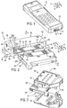
- Fig. 1 illustrates a portable cellular telephone 10 which has a receptacle connector 12 with a row 14 of terminals for mating with contacts of a plug connector, by insertion of the plug connector into a cavity 16 of the receptacle connector.
- the width in a lateral direction L is determined to a large extent by the size and number of terminals in the row 14.
- the height in a vertical direction V and the depth in forward and rearward directions F, R of the receptacle connector should be as small as possible in order to allow room for circuitry in the telephone. This is especially so as portable telephones become smaller.
- the receptacle connector 12 is manufactured by a connector manufacturer, for a telephone manufacturer who assembles the receptacle connector to a circuit board of the telephone.
- the telephone manufacturer designs the size and shape of the telephone molded casing 20, which may vary from one telephone manufacturer to the other. For this reason, the front portion of the mating plug connector should fit solely into the cavity 16, and not include any portion that attempts to
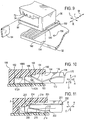
- Fig. 2 shows greater details of the receptacle connector 12 and of a mating plug connector 30.
- the receptacle connector includes a circuit board 32 and particularly an edge section 34 of the circuit board, which lies under a receptacle housing 36.
- the circuit board has an upper face 40 and has a plurality of electrically conductive traces 42 thereon arranged in the row 14.
- the receptacle housing 36 has a top wall 44 lying a distance above the traces 42, and having laterally-spaced opposite top wall sides 46, 48 with side walls 50, 52 thereat that rest on the circuit board.
- the housing also can be provided with a front wall 54 and with a rear lip 56 to lie over the rear edge of the circuit board.
- the lip is thin, with a longitudinal (M) thickness no more than the minimum height (A) of the cavity that receives the contacts.
- the plug connector 30 has a row of plug contacts 60 which are designed to engage the row of traces 42 when the connectors mate.
- the plug connector has a plug housing 62 with a laterally-extending row of plate-like separators 64 that separate the plug contacts 60.
- the top wall 44 of the receptacle housing has a laterally-extending row 70 of downwardly-extending ribs 72.
- the ribs are laterally spaced apart to leave slots 74 between them.
- the plate-like separators 64 are designed to fit into the slots 74 as the connectors mate.
- the engagement of the separators 64 in the slots 74 are preferably relied upon to precisely locate the connectors in the lateral direction L, to assure that each plug contact 60 engages only a predetermined one of the terminals formed by the traces 42. It is noted that the terminals formed by the traces 42 extend to other circuitry on the circuit board and to electrical components on the board.
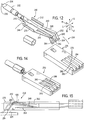
- Fig. 3 shows that the plug connector 30 has a front end portion 80 that is designed to be received in the cavity of the receptacle connector, and has a rear portion 82 that can be protected by upper and lower clam shells 84, 86 of a clam shell assembly 90.
- the clam shell assembly includes a latch actuator 92 that can operate a latch strip 94 to latch a plug connector assembly 96 that includes the plug connector 30, to the receptacle connector 12.
- the clam shell assembly 90, latch actuator 92, and latch strip 94 are known in the prior art, and are not discussed in detail herein.
- Fig. 5 shows the plug connector 30 after it has been moved in a forward direction F (which is parallel to a longitudinal direction M) far enough to only partially mate with the receptacle connector 12.
- the plug contact 60 is formed from a metal strip such as a plated copper alloy strip that has been bent.
- the contact has a rear portion 100 that is fixed to the plug housing 62 as by molding it in place.
- the contact rear portion is shown in a simplified view wherein it is crimped to a cable wire 102, although this is well known in the prior art.
- the contact has a middle portion 104 that extends primarily horizontally, to lie between the top and bottom 106, 108 of the separators 64.
- the contact has a front portion 110 which is the portion that enters the receptacle connector cavity 16 in the fully mated positions of the connectors.
- the front portion includes an upper cam-follower location 112 which can be depressed, and a lower trace-engaging location 114 which engages a receptacle terminal formed by a circuit board trace.
- the ribs 72 of the receptacle top wall form cam locations, or cam surfaces 120 that are designed to engage the cam follower locations 112 of the plug contacts as the contacts are inserted.
- the ribs also form substantially horizontal holdown surfaces 122 that engage the cam follower location 112 after the contacts have been fully mated as in Fig. 4.
- the ribs have substantially horizontal rear end surfaces 123 that extend rearwardly from the upper ends 125 of the cam surfaces.
- Each contact front portion 110 includes a rearward first part 140 that merges with the contact middle portion 104, with the first part extending at a forward-upward incline.
- the forward portion has a second part 142 at the front end of the first part, with the second part 142 forming a bend, preferably at an obtuse angle, and with the upper surface of the bend being convex and forming the cam follower location 112.
- the contact front portion includes a third part 144 that extends at a forward-downward incline from the second part, to a fourth part 146 that has a bend with a convex lower surface that forms the trace-engaging location 114.
- the angle B of the third part 144 with a horizontal direction determines, to some extent, the required depth E in the forward-rearward directions F, R of the receptacle. Applicant prefers that the angle B be at least 20° to limit the depth of the receptacle connector and to assure a firm downward force of the trace-engaging location 114 against the circuit board trace. Applicant prefers an angle B of about 30° to provide moderate resilience.
- the cam surface 120 preferably extends at a slightly greater angle of incline to the horizontal than angle B, in order to engage the middle of the contact second part 142.
- the cam surface 120 is positioned so the center 120 C along its length as seen in Fig 4, initially engages the cam follower location 112, to engage such locations for contacts that are slightly higher or lower than the designed height.
- the contacts achieve the positions shown in Fig. 4, with the cam follower locations 112 being pressed down by the holdown surfaces 122 while the locations 112 engage the circuit board traces.
- the separators 64 lie in planes such as 148 that extend geometrically normal to the lateral direction I.
- the separators are laterally spaced apart to leave gaps 140 between them, in which the contacts 60 lie.
- the lateral position of the plug connector be determined by the engagement of the separators 64 with the walls of the slots 74 (Fig. 7) in the receptacle housing top wall 44.
- Each gap 140 and the contact 60 therein lies directly under one of the top wall ribs 72. Lateral location by means of separators engaging walls of the top wall slots, assures precision alignment.
- each separator is considerably less than the width of each slot 74 to allow all separators to enter all slots despite tolerances.
- the receptacle housing 36 be mounted with precision on the circuit board, to assure that each rib 72 lies directly over a corresponding trace 42.
- Fig. 9 shows that the receptacle housing 36 is provided with downwardly-projecting posts 150, 152 that are closely received in holes 154, 156 formed in the circuit board 32.
- the hole 154 at the rear edge of the circuit board is in the form of a slot, with the post 150 being very closely laterally positioned within the slot 154.
- the forward post 152 does not need to provide as accurate an alignment.
- the lip 56 is provided to cover the rear edge 160 of the circuit board, to provide a bevel therein for plug insertion, and to provide a surface that is smooth as compared to a possibly rough cut surface of a circuit board.
- Fig. 10 illustrates another form of contact 170 with a differently formed front portion 172.
- the front portion 172 includes a first part 174 that extends at a forward-downward incline from a contact middle portion 176.
- a second part 180 forms a bend with a convex lower surface forming a trace-engaging location 182.
- a third part 184 extends at a forward-upward incline, to a fourth part 186.
- the fourth part 186 forms a bend with a convex upper surface forming a cam follower location 188.
- Fig. 10 shows, in solid lines, the cam follower location 188 when it first engages a cam surface 190.
- FIG. 10 also shows, in phantom lines, the contact front portion at 172A in the fully inserted position, wherein the trace-engaging location at 182A engages the trace and the cam follower location at 188A engages a holdown surface 192.
- the contact of Fig. 10 has an advantage in that the cam follower location 188 is forward of trace-engaging location 182 (which must be kept clean for low resistance contact and which is protected by lying more rearward). However, the contact of Fig. 10 requires a considerably longer (in forward-rearward directions) receptacle housing 198.
- Fig. 11 shows another contact 200 which has a primarily horizontal middle portion 201 whose front merges with a front portion 203 (the portion that finally enters the receptacle cavity) of the contact.
- the contact front portion has a primarily and substantially horizontal first part 205, and has a second part 202 extending in about a 170° loop, with the upper part of the loop at 204 extending largely horizontally and forming a cam-follower location.
- the lower end 206 of the loop extends at about a 10° incline (less than 60° and preferably less than 40°) from the horizontal.
- the contact front portion also has a third part 210 that extends at a rearward-downward incline to a fourth part 212 that has a bend with a convex lower surface 214 forming a trace-engaging location.
- a third part 210 that extends at a rearward-downward incline to a fourth part 212 that has a bend with a convex lower surface 214 forming a trace-engaging location.
- the contact 200 is more expensive to construct because of the large bending at the loop 202. More predicable contact deflection is achieved by providing an upward bump such as at 216 at or slightly rearward (less than the height A of the rear of the cavity) of the top of the loop.
- Fig. 2 shows that one side of the receptacle connector 12 includes three circuit board traces 221-223 that are separated from the other traces 42, while the plug connector 30 also has a separate coax section 230 at one side.
- the plug coax section 230 is constructed to connect to a shielded contact arrangement (usually a coaxial cable, but possibly a strip line or the like) while the three circuit board traces 221-223 are designed to mate to contacts of the coax section. It is noted that the traces 221 and 223 are grounded, while the trace 222 is intended to carry high frequency signals. Referring to Figs.
- the coax section 230 of the plug connector is designed to be connected to a coaxial cable 232 of the usual type that includes a grounded outer conductor 234 (which is covered by a protective jacket) and a signal-carrying inner conductor 236.
- the grounded outer conductor 234 is connected to a ground conductor arrangement 240 which includes a tab 242 extending to a ground plate portion 244, and a pair of laterally-spaced ground contacts 246, 248 that project forwardly from the ground plate portion.
- the tab 242, plate portion 244 and contacts 246, 248 are integral.
- Each of the ground contacts 246, 248 have front portions 250 with cam follower locations 252 that are designed to be downwardly deflected by a cam surface
- the front portions each have a trace-engaging location 254 that is designed to engage one of the ground traces 221, 223 of the receptacle connector.
- the coax section also includes a middle or signal contact 260 that is connected to the inner conductor 236 of the coaxial cable and which extends forwardly therefrom.
- the signal contact 260 extends over the ground plate portion 244 and between the ground contacts 246, 248.
- a front portion 262 of the signal contact lies between the front portions 250 of the ground contacts.
- the ground conductor arrangement 240 includes a grounded tine 264 that extends forwardly from the ground plate portion 244, and which lies under the signal contact 260.
- the tine 264 provides a ground plane under the elongated portion of the signal contact that extends forwardly of the ground plane portion 244, just as the ground plane portion 244 and tab 242 lie closely under more rearward portions of the signal contact.
- applicant maintains the characteristic impedance of the coaxial arrangement, while also helping to protect the signal contact 60 from stray electromagnetic radiation.
- the presence of the ground conductors 246, 248 on laterally opposite sides of the signal contact also aids in maintaining characteristic impedance and avoiding stray signals.
- the signal contact 260 and ground conductor arrangement 240 are mounted in a dielectric coax frame 274 which has forward walls forming a group of locating spacers 276 that are similar to the spacers 64 described in the connection with Fig. 2.
- the spacers form a middle coax gap 280 that holds the front portion of the signal contact and a pair of side coax gaps 282, 284 that hold the front portions of the ground contacts.
- coax does not refer solely to a coaxial arrangement, but to a shielding arrangement that can connect to a coaxial cable.
- FIG. 15 shows the manner in which the cam follower 252 of a ground conductor front portion 250 is downwardly deflected by a cam surface 120 until the trace-engaging location 254 engages a grounded trace such as 221, during mating of the plug and receptacle connectors.
- the area of the circuit board, or edge section 34 (Fig. 2) available for holding the receptacle housing 36 was only 25 millimeters wide (in direction L) and 10 millimeters deep (in directions F, R).
- the available height above the circuit board face 40 was only 5 millimeters.
- the traces 42 were spaced (center-to-center) by only one millimeter. It can be appreciated that precision assembly is required to assure that all contacts engage only a single selected circuit board trace.
- the invention provides a connector system wherein the receptacle connector has a small depth and height, the receptacle connector can be precisely constructed at low cost, and the plug and receptacle connectors can be mated with no part of the plug connector required to surround the receptacle connector.
- the receptacle connector includes a circuit board with a row of traces thereon and also includes a receptacle housing having a top wall lying above the traces.
- the plug connector has a front portion that fits into the space between the top wall and circuit board of the receptacle connector, and has a plurality of plug contacts with front portions for engaging the traces.
- the top wall of the receptacle housing has a row of cam surfaces positioned to depress cam-follower locations on the plug contacts until trace-engaging locations on the plug contacts engage the traces.
- the plug housing has a plurality of plate-like separators separating the plug contacts, and the top wall of the receptacle has downwardly-depending ribs that are spaced to form slots that receive the spacers, and with the ribs having lower surfaces forming the cam surfaces for depressing the plug contacts.
- the invention also provides the plug connector with a coax section that includes contacts similar to those for the rest of the connector, but which provide a ground plane and other ground surfaces lying closely beside the signal contact. A pair of ground contacts lie on laterally opposite sides of the signal contact. A grounded tine lies under much of the signal contact.
Applications Claiming Priority (2)
| Application Number | Priority Date | Filing Date | Title |
|---|---|---|---|
| US08/741,758 US5807126A (en) | 1996-11-05 | 1996-11-05 | Low profile connector system |
| US741758 | 1996-11-05 |
Publications (2)
| Publication Number | Publication Date |
|---|---|
| EP0840399A2 true EP0840399A2 (de) | 1998-05-06 |
| EP0840399A3 EP0840399A3 (de) | 1999-08-18 |
Family
ID=24982055
Family Applications (1)
| Application Number | Title | Priority Date | Filing Date |
|---|---|---|---|
| EP97118861A Withdrawn EP0840399A3 (de) | 1996-11-05 | 1997-10-30 | Flachprofilverbindersystem |
Country Status (7)
| Country | Link |
|---|---|
| US (1) | US5807126A (de) |
| EP (1) | EP0840399A3 (de) |
| JP (1) | JP2911860B2 (de) |
| KR (1) | KR100291847B1 (de) |
| CN (1) | CN1182291A (de) |
| CA (1) | CA2218996A1 (de) |
| TW (1) | TW373355B (de) |
Cited By (6)
| Publication number | Priority date | Publication date | Assignee | Title |
|---|---|---|---|---|
| WO2000008722A1 (en) * | 1998-08-05 | 2000-02-17 | Ericsson, Inc. | Moisture resistant electrical connector for a cellular telephone |
| EP1065758A2 (de) * | 1999-06-28 | 2001-01-03 | Itt Manufacturing Enterprises, Inc. | IC-Karte mit hinterem Verbinder zum Aufnahme eines Steckers |
| DE10048457A1 (de) * | 2000-09-29 | 2002-05-02 | Siemens Ag | Anordnung und Verfahren zum Kontaktieren eines Motor- oder Getriebebauteils an eine elektrische Leiterplatte |
| EP1328043A1 (de) * | 2002-01-10 | 2003-07-16 | Osram Sylvania, Inc. | Ein Verbinderstift für Leiterplattenränder |
| GB2435553A (en) * | 2006-02-22 | 2007-08-29 | Itt Mfg Enterprises Inc | Multiple coaxial connector |
| EP2083555A2 (de) * | 2008-01-28 | 2009-07-29 | Tyco Electronics AMP Korea Limited | Wasserdichtheitsverfahren und Struktur für ein Mobiltelefon |
Families Citing this family (20)
| Publication number | Priority date | Publication date | Assignee | Title |
|---|---|---|---|---|
| JP3594434B2 (ja) * | 1997-01-08 | 2004-12-02 | ヒロセ電機株式会社 | 回路基板への電気コネクタ取付構造 |
| US6052314A (en) * | 1997-05-22 | 2000-04-18 | Rohm Co., Ltd. | EEPROM device |
| US6007359A (en) * | 1997-11-25 | 1999-12-28 | Itt Manufacturing Enterprises, Inc. | Receptacle connector |
| US5899759A (en) * | 1997-12-29 | 1999-05-04 | Ford Motor Company | Electrical connector for rigid circuit boards |
| US6373259B1 (en) * | 1999-03-09 | 2002-04-16 | Avaya Technology Corp. | Connector testing system having a test prong including a projection |
| US6422900B1 (en) | 1999-09-15 | 2002-07-23 | Hh Tower Group | Coaxial cable coupling device |
| US6413103B1 (en) | 2000-11-28 | 2002-07-02 | Apple Computer, Inc. | Method and apparatus for grounding microcoaxial cables inside a portable computing device |
| US6764344B2 (en) | 2001-07-02 | 2004-07-20 | Seagate Technology Llc | Disc drive circuit board edge connector |
| CN1437089B (zh) * | 2002-02-05 | 2012-01-25 | 劲永科技(苏州)有限公司 | 用于usb介面的连接装置及其储存器储存装置 |
| US20050095902A1 (en) * | 2003-11-04 | 2005-05-05 | Hongbo Zhang | Connector assembly |
| KR100968327B1 (ko) | 2007-03-14 | 2010-07-08 | 파나소닉 전공 주식회사 | 다극동축커넥터 |
| JP5094604B2 (ja) * | 2008-07-14 | 2012-12-12 | 矢崎総業株式会社 | インナーターミナル |
| JP6350876B2 (ja) * | 2015-06-18 | 2018-07-04 | 株式会社オートネットワーク技術研究所 | コネクタ |
| DE102017115225A1 (de) * | 2016-07-08 | 2018-01-11 | Hirschmann Car Communication Gmbh | Kabelmontage für Koaxialkabel auf dicken Leiterplatten |
| JP6542921B2 (ja) * | 2018-01-19 | 2019-07-10 | モレックス エルエルシー | コネクタ |
| CN108201230B (zh) * | 2018-01-30 | 2020-11-03 | 黑龙江工业学院 | 一种语言教学用多媒体电教台 |
| JP7340220B2 (ja) * | 2018-12-03 | 2023-09-07 | 日本圧着端子製造株式会社 | 複合コネクタ |
| CN111755916B (zh) | 2019-03-28 | 2022-02-08 | 莫仕连接器(成都)有限公司 | 电连接器 |
| TWI740710B (zh) * | 2020-11-10 | 2021-09-21 | 財團法人工業技術研究院 | 具改善端子共面度之連接器結構 |
| CN113161815B (zh) * | 2021-03-23 | 2022-07-05 | 深圳市威特利电源有限公司 | 移动电源智能充放电控制方法和系统 |
Citations (10)
| Publication number | Priority date | Publication date | Assignee | Title |
|---|---|---|---|---|
| US3689865A (en) * | 1968-03-11 | 1972-09-05 | Texas Instruments Inc | Connector |
| US4169644A (en) * | 1976-03-11 | 1979-10-02 | Bonhomme F R | Electrical connection devices |
| US4550959A (en) * | 1983-04-13 | 1985-11-05 | Amp Incorporated | Surface mountable coefficient of expansion matching connector |
| EP0168922A2 (de) * | 1984-07-16 | 1986-01-22 | Trw Inc. | Ohne Einführungskraft kontaktierbarer Steckverbinder |
| EP0251508A1 (de) * | 1986-06-26 | 1988-01-07 | Amp Incorporated | Null-Einschubskraft-Schaltkartensteckverbinder |
| EP0423459A2 (de) * | 1989-10-16 | 1991-04-24 | International Business Machines Corporation | Faseroptische Verbindungsanordnung |
| US5035641A (en) * | 1988-02-15 | 1991-07-30 | Itt Industries Limited | Terminating insulated conductors |
| US5062809A (en) * | 1990-03-15 | 1991-11-05 | Amp Incorporated | High-frequency connector and method of manufacturing thereof |
| US5176535A (en) * | 1990-05-30 | 1993-01-05 | Amp Incorporated | Electrical connector and cable utilizing spring grade wire |
| US5281150A (en) * | 1993-01-05 | 1994-01-25 | International Business Machines Corporation | Method and apparatus for connecting cable to the surface of printed circuit boards or the like |
Family Cites Families (17)
| Publication number | Priority date | Publication date | Assignee | Title |
|---|---|---|---|---|
| US2857577A (en) * | 1955-11-01 | 1958-10-21 | Hughes Aircraft Co | Electrical connector |
| US3217285A (en) * | 1964-12-22 | 1965-11-09 | Sylvania Electric Prod | Positive pressure connector |
| GB1154367A (en) * | 1965-10-14 | 1969-06-04 | Lucas Industries Ltd | Connectors for use with Flexible and Rigid Printed Circuits |
| US3474387A (en) * | 1967-04-13 | 1969-10-21 | Elco Corp | Zero insertion force connector and contact therefor |
| JPS5544429B2 (de) * | 1973-05-11 | 1980-11-12 | ||
| US4017696A (en) * | 1975-12-31 | 1977-04-12 | Bell Telephone Laboratories, Incorporated | Initializing circuit |
| US4542950A (en) * | 1984-02-21 | 1985-09-24 | International Business Machines Corporation | Zero insertion force edge connector with wipe cycle |
| JPS6111284U (ja) * | 1984-06-26 | 1986-01-23 | 沖電線株式会社 | 基板接続コネクタ |
| US4640562A (en) * | 1984-12-19 | 1987-02-03 | Amp Incorporated | Surface mounting means for printed circuit board |
| US4776803A (en) * | 1986-11-26 | 1988-10-11 | Minnesota Mining And Manufacturing Company | Integrally molded card edge cable termination assembly, contact, machine and method |
| US4768971A (en) * | 1987-07-02 | 1988-09-06 | Rogers Corporation | Connector arrangement |
| US4919626A (en) * | 1989-04-14 | 1990-04-24 | Itt Corporation | Connector for IC card |
| US5015197A (en) * | 1990-05-30 | 1991-05-14 | Amp Incorporated | Electrical connector and cable utilizing spring grade wire |
| JP2793380B2 (ja) * | 1991-06-17 | 1998-09-03 | 富士通株式会社 | 同軸マルチ混在コネクタ |
| JP2598581Y2 (ja) * | 1991-12-03 | 1999-08-16 | 矢崎総業株式会社 | コネクタ |
| US5383788A (en) * | 1993-05-20 | 1995-01-24 | W. L. Gore & Associates, Inc. | Electrical interconnect assembly |
| US5391089A (en) * | 1993-08-26 | 1995-02-21 | Becton, Dickinson And Company | Cam action electrical edge connector |
-
1996
- 1996-11-05 US US08/741,758 patent/US5807126A/en not_active Expired - Fee Related
-
1997
- 1997-10-21 CA CA002218996A patent/CA2218996A1/en not_active Abandoned
- 1997-10-30 EP EP97118861A patent/EP0840399A3/de not_active Withdrawn
- 1997-11-04 CN CN97121592A patent/CN1182291A/zh active Pending
- 1997-11-05 JP JP9303067A patent/JP2911860B2/ja not_active Expired - Lifetime
- 1997-11-05 KR KR1019970058102A patent/KR100291847B1/ko not_active IP Right Cessation
- 1997-11-05 TW TW086116488A patent/TW373355B/zh active
Patent Citations (10)
| Publication number | Priority date | Publication date | Assignee | Title |
|---|---|---|---|---|
| US3689865A (en) * | 1968-03-11 | 1972-09-05 | Texas Instruments Inc | Connector |
| US4169644A (en) * | 1976-03-11 | 1979-10-02 | Bonhomme F R | Electrical connection devices |
| US4550959A (en) * | 1983-04-13 | 1985-11-05 | Amp Incorporated | Surface mountable coefficient of expansion matching connector |
| EP0168922A2 (de) * | 1984-07-16 | 1986-01-22 | Trw Inc. | Ohne Einführungskraft kontaktierbarer Steckverbinder |
| EP0251508A1 (de) * | 1986-06-26 | 1988-01-07 | Amp Incorporated | Null-Einschubskraft-Schaltkartensteckverbinder |
| US5035641A (en) * | 1988-02-15 | 1991-07-30 | Itt Industries Limited | Terminating insulated conductors |
| EP0423459A2 (de) * | 1989-10-16 | 1991-04-24 | International Business Machines Corporation | Faseroptische Verbindungsanordnung |
| US5062809A (en) * | 1990-03-15 | 1991-11-05 | Amp Incorporated | High-frequency connector and method of manufacturing thereof |
| US5176535A (en) * | 1990-05-30 | 1993-01-05 | Amp Incorporated | Electrical connector and cable utilizing spring grade wire |
| US5281150A (en) * | 1993-01-05 | 1994-01-25 | International Business Machines Corporation | Method and apparatus for connecting cable to the surface of printed circuit boards or the like |
Cited By (10)
| Publication number | Priority date | Publication date | Assignee | Title |
|---|---|---|---|---|
| WO2000008722A1 (en) * | 1998-08-05 | 2000-02-17 | Ericsson, Inc. | Moisture resistant electrical connector for a cellular telephone |
| US6227872B1 (en) | 1998-08-05 | 2001-05-08 | Ericsson Inc. | Moisture resistant electrical connector for a cellular telephone |
| EP1065758A2 (de) * | 1999-06-28 | 2001-01-03 | Itt Manufacturing Enterprises, Inc. | IC-Karte mit hinterem Verbinder zum Aufnahme eines Steckers |
| EP1065758A3 (de) * | 1999-06-28 | 2003-01-15 | Itt Manufacturing Enterprises, Inc. | IC-Karte mit hinterem Verbinder zum Aufnahme eines Steckers |
| DE10048457A1 (de) * | 2000-09-29 | 2002-05-02 | Siemens Ag | Anordnung und Verfahren zum Kontaktieren eines Motor- oder Getriebebauteils an eine elektrische Leiterplatte |
| DE10048457B4 (de) * | 2000-09-29 | 2004-07-08 | Siemens Ag | Anordnung und Verfahren zum Kontaktieren eines Motor- oder Getriebebauteils an eine elektrische Leiterplatte |
| EP1328043A1 (de) * | 2002-01-10 | 2003-07-16 | Osram Sylvania, Inc. | Ein Verbinderstift für Leiterplattenränder |
| GB2435553A (en) * | 2006-02-22 | 2007-08-29 | Itt Mfg Enterprises Inc | Multiple coaxial connector |
| EP2083555A2 (de) * | 2008-01-28 | 2009-07-29 | Tyco Electronics AMP Korea Limited | Wasserdichtheitsverfahren und Struktur für ein Mobiltelefon |
| EP2083555A3 (de) * | 2008-01-28 | 2011-09-07 | Tyco Electronics AMP Korea Limited | Wasserdichtheitsverfahren und Struktur für ein Mobiltelefon |
Also Published As
| Publication number | Publication date |
|---|---|
| CA2218996A1 (en) | 1998-05-05 |
| EP0840399A3 (de) | 1999-08-18 |
| JPH10228962A (ja) | 1998-08-25 |
| KR19980042084A (ko) | 1998-08-17 |
| US5807126A (en) | 1998-09-15 |
| CN1182291A (zh) | 1998-05-20 |
| JP2911860B2 (ja) | 1999-06-23 |
| KR100291847B1 (ko) | 2001-06-01 |
| TW373355B (en) | 1999-11-01 |
Similar Documents
| Publication | Publication Date | Title |
|---|---|---|
| US5807126A (en) | Low profile connector system | |
| US10847936B2 (en) | Card edge connector with improved grounding member | |
| US7311552B1 (en) | Micro coaxial cable connector assembly | |
| US7384310B2 (en) | Electrical connector with reliable structure and method for making the same | |
| US8961235B2 (en) | Electrical connector with improved mating member having anti-mismating portion for preventing incorrect insertion | |
| US7008267B2 (en) | Shielded board-mounted electrical connector | |
| US6338652B1 (en) | Low profile cable connector with grounding means | |
| US4838811A (en) | Modular connector with EMI countermeasure | |
| US7229298B2 (en) | Electrical connector having an improved grounding path | |
| EP0165490B1 (de) | Auf einer gedruckten Schaltungskarte befestigter Aufnahmestecker für einen am Ende eines Kabels befestigten modularen Steckverbinder | |
| US6007359A (en) | Receptacle connector | |
| US6210230B1 (en) | Cable connector | |
| US5997329A (en) | Enhanced connector system | |
| EP0624928B1 (de) | Abgeschirmte elektrische Verbinderanordnung | |
| US6752658B2 (en) | Low crosstalk insulation displacement connector for terminating cable to circuit board | |
| US6893272B2 (en) | Electrical connector assembly having improved grounding means | |
| US6749463B1 (en) | Shielded board mounted electrical connector | |
| US7357679B2 (en) | Cable connector with improved terminals | |
| EP0996993B1 (de) | Verriegelte und abgeschirmte elektrische verbinder | |
| US7618268B2 (en) | Electrical connector with reliable mating frame mating with another connector | |
| US7517249B1 (en) | Electrical connector assembly having retention structure | |
| US6971923B1 (en) | Cable end connector assembly with improved organizer | |
| US6183281B1 (en) | Electrical connector | |
| US6780063B2 (en) | Wire connected modular jack and assembling method | |
| US20070087595A1 (en) | Electrical connector with improved housing |
Legal Events
| Date | Code | Title | Description |
|---|---|---|---|
| PUAI | Public reference made under article 153(3) epc to a published international application that has entered the european phase |
Free format text: ORIGINAL CODE: 0009012 |
|
| AK | Designated contracting states |
Kind code of ref document: A2 Designated state(s): DE FI FR GB IT SE |
|
| PUAL | Search report despatched |
Free format text: ORIGINAL CODE: 0009013 |
|
| AK | Designated contracting states |
Kind code of ref document: A3 Designated state(s): AT BE CH DE DK ES FI FR GB GR IE IT LI LU MC NL PT SE |
|
| 17P | Request for examination filed |
Effective date: 20000218 |
|
| AKX | Designation fees paid |
Free format text: DE FI FR GB IT SE |
|
| 17Q | First examination report despatched |
Effective date: 20030918 |
|
| STAA | Information on the status of an ep patent application or granted ep patent |
Free format text: STATUS: THE APPLICATION IS DEEMED TO BE WITHDRAWN |
|
| 18D | Application deemed to be withdrawn |
Effective date: 20050913 |