EP0836713B1 - Kamera-system - Google Patents
Kamera-system Download PDFInfo
- Publication number
- EP0836713B1 EP0836713B1 EP96920990A EP96920990A EP0836713B1 EP 0836713 B1 EP0836713 B1 EP 0836713B1 EP 96920990 A EP96920990 A EP 96920990A EP 96920990 A EP96920990 A EP 96920990A EP 0836713 B1 EP0836713 B1 EP 0836713B1
- Authority
- EP
- European Patent Office
- Prior art keywords
- image
- radiation
- charge
- image intensifier
- fluorescent screen
- Prior art date
- Legal status (The legal status is an assumption and is not a legal conclusion. Google has not performed a legal analysis and makes no representation as to the accuracy of the status listed.)
- Expired - Lifetime
Links
- 230000005855 radiation Effects 0.000 claims description 38
- OAICVXFJPJFONN-UHFFFAOYSA-N Phosphorus Chemical compound [P] OAICVXFJPJFONN-UHFFFAOYSA-N 0.000 claims description 10
- 238000009416 shuttering Methods 0.000 claims description 2
- 230000001052 transient effect Effects 0.000 claims description 2
- XUIMIQQOPSSXEZ-UHFFFAOYSA-N Silicon Chemical compound [Si] XUIMIQQOPSSXEZ-UHFFFAOYSA-N 0.000 description 7
- 229910052710 silicon Inorganic materials 0.000 description 7
- 239000010703 silicon Substances 0.000 description 7
- 230000004888 barrier function Effects 0.000 description 5
- 229910021420 polycrystalline silicon Inorganic materials 0.000 description 5
- 229920005591 polysilicon Polymers 0.000 description 5
- 238000002474 experimental method Methods 0.000 description 4
- 238000010586 diagram Methods 0.000 description 3
- 230000002452 interceptive effect Effects 0.000 description 3
- 239000002245 particle Substances 0.000 description 3
- 239000004411 aluminium Substances 0.000 description 2
- 229910052782 aluminium Inorganic materials 0.000 description 2
- XAGFODPZIPBFFR-UHFFFAOYSA-N aluminium Chemical compound [Al] XAGFODPZIPBFFR-UHFFFAOYSA-N 0.000 description 2
- 230000004907 flux Effects 0.000 description 2
- 230000005865 ionizing radiation Effects 0.000 description 2
- 229910052751 metal Inorganic materials 0.000 description 2
- 239000002184 metal Substances 0.000 description 2
- 238000000034 method Methods 0.000 description 2
- JJWKPURADFRFRB-UHFFFAOYSA-N carbonyl sulfide Chemical compound O=C=S JJWKPURADFRFRB-UHFFFAOYSA-N 0.000 description 1
- 239000002131 composite material Substances 0.000 description 1
- 230000001419 dependent effect Effects 0.000 description 1
- 238000005286 illumination Methods 0.000 description 1
- 238000003384 imaging method Methods 0.000 description 1
- 230000003993 interaction Effects 0.000 description 1
- VIKNJXKGJWUCNN-XGXHKTLJSA-N norethisterone Chemical compound O=C1CC[C@@H]2[C@H]3CC[C@](C)([C@](CC4)(O)C#C)[C@@H]4[C@@H]3CCC2=C1 VIKNJXKGJWUCNN-XGXHKTLJSA-N 0.000 description 1
- 230000003071 parasitic effect Effects 0.000 description 1
- 239000007787 solid Substances 0.000 description 1
- 230000003068 static effect Effects 0.000 description 1
Images

Classifications
-
- G—PHYSICS
- G01—MEASURING; TESTING
- G01T—MEASUREMENT OF NUCLEAR OR X-RADIATION
- G01T1/00—Measuring X-radiation, gamma radiation, corpuscular radiation, or cosmic radiation
- G01T1/29—Measurement performed on radiation beams, e.g. position or section of the beam; Measurement of spatial distribution of radiation
- G01T1/2914—Measurement of spatial distribution of radiation
- G01T1/2921—Static instruments for imaging the distribution of radioactivity in one or two dimensions; Radio-isotope cameras
- G01T1/2928—Static instruments for imaging the distribution of radioactivity in one or two dimensions; Radio-isotope cameras using solid state detectors
-
- G—PHYSICS
- G01—MEASURING; TESTING
- G01V—GEOPHYSICS; GRAVITATIONAL MEASUREMENTS; DETECTING MASSES OR OBJECTS; TAGS
- G01V5/00—Prospecting or detecting by the use of ionising radiation, e.g. of natural or induced radioactivity
- G01V5/20—Detecting prohibited goods, e.g. weapons, explosives, hazardous substances, contraband or smuggled objects
Definitions
- the current invention relates to a camera system for making video images of moving or still objects illuminated by pulsed gamma or neutron radiation.
- Solid state charge coupled device “CCD” cameras when used in a high energy gamma or neutron radiation environment (whether pulsed or not) suffer from radiation induced artefacts. These artefacts are caused by scattered gamma or neutron radiation and are referred to by those skilled in the art as gamma induced back ground or neutron stars. These artefacts arise when the scattered gamma or neutron radiation passes through the camera structure to directly affect an imaging sensor within the camera. As a result an image produced by the sensor lacks purity because of these radiation induced artefacts. In some circumstances the image is totally masked by the artefacts. Shielding the camera from the source of radiation in many instances is either impractical or ineffective.
- the objective of the of the invention is to remove from the final image produced by the TV camera the spurious signals caused by the scattered radiation interfering with the TV sensor.
- spurious signals arise in the case of the ionizing radiation in the form of a photo charge but cause no permanent damage.
- the high energy particles they can cause localised current spikes and are stored within the TV sensor also as a photo-charge. For example collisions between neutrons and silicon nuclei produce photo charge artefacts known as neutron stars.
- the Applicant has found that the high energy particles produce no permanent damage possibly as a result of restricting the accumulated dose to the TV sensor when a pulsed source of radiation is used.
- a light image on the TV sensor is absorbed by a silicon layer to give rise to an electron and hole pair of which the electron is subsequently collected by a polysilicon electrode structure within the CCD device to generate a photo signal.
- the depth at which the electrons are produced is dependent on the wave length of the light but 90% of all light at 400nm is absorbed within the first 25 micrometers of silicon and 90% of all light at 900 nm is absorbed within the first 60 micrometers of silicon. Thus only a thin silicon layer is required to absorb and detect the visible illumination.
- an apparatus for recording a transient radiation event consisting of direct and scattered radiation having a first fluorescent screen producing a light image of the direct radiation and a television camera arranged to receive the light image having a charged coupled device within which is an anti-blooming gate characterised in that the anti-blooming gate within the charge coupled device is configured such that rapidly applying positive charge to the electrode removes negative photo charge caused by impinging scattered radiation; and in that a shutter means is placed between the fluorescent screen and the television camera with the shutter means is arranged such that opening the shutter after the photo charge has been removed allows the television camera to record the light image formed on the fluorescent screen.
- the advantage of this arrangement is that the unwanted artefacts resulting from the spurious radiation signals are removed so that a high quality image is produced by the TV camera of a scene of interest.
- the direct radiation is radiation reflected from the scene of interest and arises from a source of pulsed radiation and comprises high energy photons (ionizing radiation for example gamma rays, x-rays, cosmic rays) or high energy particles for example neutrons or protons.
- high energy photons ionizing radiation for example gamma rays, x-rays, cosmic rays
- high energy particles for example neutrons or protons.
- the scattered radiation arises from the same source as the direct radiation but is scattered such that some of the radiation may pass through the TV camera structure to interfere with the TV camera sensor.
- the invention applies equally well to CCD cameras configured at normal TV scanning rates as well as fast read out CCD cameras although the invention was initially made for fast read out CCD TV cameras.
- ABG anti-blooming gate
- the Applicant has found that high energy gamma and 14 MeV neutron radiation artefacts can be completely removed from the CCD by this fast removal technique.
- Such a fast removal technique allows when the ABG is negatively pulsed for 1 microsecond to completely remove all the photo charge arising from the radiation induced artefacts.
- This parasitic charge which typically may last only for tens of nanoseconds for gamma radiation artefacts or 100 nanoseconds for neutron artefacts which may occur over a micro second window.
- the shutter means may comprise a first image intensifier and a second image intensifier the first image intensifier placed between the fluorescent screen and the second image intensifier a first phosphorescent screen of the first image intensifier having a slow decay phosphor producing a latent image of the light image on the fluorescent screen, the second image intensifier shuttering the first phosphorescent screen during the passage of the scattered radiation.
- the second phosphorescent screen of the second image intensifier may have a fast decay phosphor situated adjacent to the charge coupled device of the television camera.
- the electrode known as the anti blooming electrode which may be a structure situated within the charge coupled device comprises a transfer electrode of polysilicon, a gate of metal for example aluminium and a drain of doped or Impure silicon.
- the polysilicon transfer electrode after exposure to light or neutron or gamma radiation may collect electrons as a stored charge maintained at a predetermined level by a negative barrier potential on the gate changing the barrier potential on the gate to a positive value releases the stored electrons which flow to the drain maintained at a higher positive value.
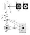
- FIG. 1 shows a schematic diagram of an experiment using a camera system according to the invention.
- a beam of direct radiation 2 and a beam of scattered radiation 4 emanate from a source of radiation 6.
- the beam of direct radiation passes through a pin hole collimator 8 (a 4mm aperture In 25 mm thick lead wall) to impinge on a fluorescent screen 10 to produce a light image 11.
- the fluorescent screen 10 having a nanosecond decay time.
- a beam of light 12 passes into a lens 14, an intensifier combination 16 and a TV camera 18.
- a video signal 20 passes to a display 22 on a monitor 24.
- An example display 26 shows an image 28 of the scene of interest 11 and 6 with neutron or gamma artefacts 30 interfering with the image 28.
- An example display 32 shows an image of the scene of interest 11 and 6 with out neutron or gamma artefacts interfering with the image 28.
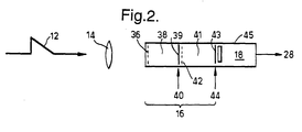
- the image intensifier combination 16 comprises a first image intensifier 38 consisting of a micro-channel plate intensifier known to those skilled in the art as a Generation 2 or GEN 2 intensifier, and a second image intensifier 41 consisting of a cross over tube image intensifier known to those skilled in the art as a Generation 1 intensifier or GEN 1 intensifier.
- the GEN 2 intensifier 38 is mounted in front of the GEN 1 intensifier 41 as follows.
- Light 12 from the fluorescent screen 10 shown on Figure 1 passes through the lens 14 to fall on a first photo cathode 36 to produce a second light image 39 on the first phosphorescent (phosphor) screen 40 comprising a slow (milli second) decay phosphor known to those skilled in the art as a P20 phosphor.
- the second light image 39 is then recorded by the second photo cathode 42 to produce a third light image 43 on the second phosphorescent (phosphor) screen 44 comprising a fast (100s of nano seconds) decay phosphor known to those skilled in the art as a P48 phosphor.
- the third light image 43 is then recorded by the CCD 45 of the TV camera 18 to produce the video signal 28.
- the first phosphorescent screen 40 should preferably have a slow image decay rate measured in milli-seconds; and that the second phosphorescent screen 44 should preferably have a fast image decay rate measured in nano-seconds.
- a gated anti blooming structure 50 consisting of a transfer electrode 52 of polysilicon, a gate 52 of metal for example aluminium and a drain 54 of doped that is impure silicon.
- the polysilicon transfer electrode 52 after exposure to light or neutron or gamma radiation collects electrons as a stored charge 56 as explained previously and may for convenience referred to a well charge 56.
- the well charge 56 is maintained at a predetermined level by a negative barrier potential 58. Excess charge 60 flowing over the barrier 58 which for convenience can be thought of as a sluice gate in a water channel.
- the fluorescent screen 10 may be substituted by a slow fluorescer to have a slow image decay instead of a fast image decay.
Landscapes
- Physics & Mathematics (AREA)
- Life Sciences & Earth Sciences (AREA)
- General Physics & Mathematics (AREA)
- High Energy & Nuclear Physics (AREA)
- Health & Medical Sciences (AREA)
- Molecular Biology (AREA)
- Spectroscopy & Molecular Physics (AREA)
- General Life Sciences & Earth Sciences (AREA)
- Geophysics (AREA)
- Measurement Of Radiation (AREA)
- Transforming Light Signals Into Electric Signals (AREA)
- Image-Pickup Tubes, Image-Amplification Tubes, And Storage Tubes (AREA)
Claims (3)
- Vorrichtung zum Aufzeichnen eines Übergangsstrahlungsereignisses, das aus direkter (2) und gestreuter (4) Strahlung besteht, mit einem ersten fluoreszierenden Bildschirm (10), der ein Lichtbild (11) der direkten Strahlung (2) erzeugt, und einer Fernsehkamera (18), die so beschaffen ist, daß sie das Lichtbild (11) empfängt, und eine ladungsgekoppelte Vorrichtung (45) aufweist, in der sich ein Anti-Überstrahlungsgatter (52) befindet,
dadurch gekennzeichnet, daßdas Anti-Überstrahlungsgatter (52) innerhalb der ladungsgekoppelten Vorrichtung (45) so konfiguriert ist, daß das schnelle Beaufschlagen des Gatters (52) mit positiver Ladung die negative Photoladung entfernt, die durch die auftreffende gestreute Strahlung (4) hervorgerufen wird, undein Verschlußmittel (16) zwischen dem fluoreszierenden Bildschirm (10) und der Fernsehkamera (18) angeordnet und so beschaffen ist, daß das Öffnen des Verschlusses nach dem Entfernen der Photoladung der Fernsehkamera (18) ermöglicht, das auf dem fluoreszierenden Bildschirm (10) ausgebildete Lichtbild (11) aufzuzeichnen. - Vorrichtung nach Anspruch 1, dadurch gekennzeichnet, daß das Verschlußmittel (16) einen ersten Bildverstärker (38) und einen zweiten Bildverstärker (41) umfaßt, wobei der erste Bildverstärker (38) zwischen dem fluoreszierenden Bildschirm (10) und dem zweiten Bildverstärker (41) angeordnet ist, ein erster phosphoreszierender Bildschirm (40) des ersten Bildverstärkers (38) einen langsam abklingenden Phosphor aufweist, der ein latentes Bild des Lichtbildes (11) auf dem fluoreszierenden Bildschirm erzeugt und der zweite Bildverstärker (41) den ersten phosphoreszierenden Bildschirm (40) während des Durchlassens der gestreuten Strahlung (4) abblendet.
- Vorrichtung nach Anspruch 2, dadurch gekennzeichnet, daß der phosphoreszierende Bildschirm (44) des zweiten Bildverstärkers (41) mit einem schnell abklingenden Phosphor versehen ist und neben der ladungsgekoppelten Vorrichtung (45) der Fernsehkamera (18) angeordnet ist.
Applications Claiming Priority (3)
| Application Number | Priority Date | Filing Date | Title |
|---|---|---|---|
| GB9513444 | 1995-07-01 | ||
| GBGB9513444.1A GB9513444D0 (en) | 1995-07-01 | 1995-07-01 | A camera system |
| PCT/GB1996/001543 WO1997002498A1 (en) | 1995-07-01 | 1996-06-27 | A camera system |
Publications (2)
| Publication Number | Publication Date |
|---|---|
| EP0836713A1 EP0836713A1 (de) | 1998-04-22 |
| EP0836713B1 true EP0836713B1 (de) | 2001-09-26 |
Family
ID=10776995
Family Applications (1)
| Application Number | Title | Priority Date | Filing Date |
|---|---|---|---|
| EP96920990A Expired - Lifetime EP0836713B1 (de) | 1995-07-01 | 1996-06-27 | Kamera-system |
Country Status (7)
| Country | Link |
|---|---|
| US (1) | US5991359A (de) |
| EP (1) | EP0836713B1 (de) |
| JP (1) | JPH11508687A (de) |
| AU (1) | AU6236096A (de) |
| DE (1) | DE69615559T2 (de) |
| GB (1) | GB9513444D0 (de) |
| WO (1) | WO1997002498A1 (de) |
Families Citing this family (2)
| Publication number | Priority date | Publication date | Assignee | Title |
|---|---|---|---|---|
| JP2006510033A (ja) * | 2002-12-10 | 2006-03-23 | コモンウェルス サイエンティフィック アンド インダストリアル リサーチ オーガニゼーション | 放射線撮影装置 |
| JP5347921B2 (ja) * | 2009-07-27 | 2013-11-20 | 株式会社リコー | トナー挙動可視化装置 |
Family Cites Families (6)
| Publication number | Priority date | Publication date | Assignee | Title |
|---|---|---|---|---|
| US4679212A (en) * | 1984-07-31 | 1987-07-07 | Texas Instruments Incorporated | Method and apparatus for using surface trap recombination in solid state imaging devices |
| US4829552A (en) * | 1985-12-06 | 1989-05-09 | Rossi Remo J | Anti-scatter grid system |
| NL8801946A (nl) * | 1988-08-04 | 1990-03-01 | Philips Nv | Roentgenbeeldsysteem. |
| DE4306461C1 (de) * | 1993-03-02 | 1994-05-05 | Siemens Ag | Fernsehaufnahmeeinrichtung mit Halbleiter-Bildwandler |
| FR2706626B1 (fr) * | 1993-06-09 | 1995-08-04 | Stmi | Dispositif de localisation à distance de sources de rayonnement. |
| CA2126064A1 (en) * | 1993-06-17 | 1994-12-18 | Jean-Francois Meunier | Apparatus and method for converting a visible image of an object into a digital representation |
-
1995
- 1995-07-01 GB GBGB9513444.1A patent/GB9513444D0/en active Pending
-
1996
- 1996-06-27 DE DE69615559T patent/DE69615559T2/de not_active Expired - Fee Related
- 1996-06-27 JP JP9504908A patent/JPH11508687A/ja active Pending
- 1996-06-27 AU AU62360/96A patent/AU6236096A/en not_active Abandoned
- 1996-06-27 US US08/983,241 patent/US5991359A/en not_active Expired - Fee Related
- 1996-06-27 EP EP96920990A patent/EP0836713B1/de not_active Expired - Lifetime
- 1996-06-27 WO PCT/GB1996/001543 patent/WO1997002498A1/en not_active Ceased
Also Published As
| Publication number | Publication date |
|---|---|
| GB9513444D0 (en) | 1995-09-06 |
| DE69615559T2 (de) | 2002-07-11 |
| US5991359A (en) | 1999-11-23 |
| JPH11508687A (ja) | 1999-07-27 |
| DE69615559D1 (de) | 2001-10-31 |
| AU6236096A (en) | 1997-02-05 |
| EP0836713A1 (de) | 1998-04-22 |
| WO1997002498A1 (en) | 1997-01-23 |
Similar Documents
| Publication | Publication Date | Title |
|---|---|---|
| US6069362A (en) | Multi-density and multi-atomic number detector media for applications | |
| US6362484B1 (en) | Imager or particle or radiation detector and method of manufacturing the same | |
| Fan et al. | Digital imaging in transmission electron microscopy | |
| CA2270269A1 (en) | Photoconductor-photocathode imager | |
| Looker et al. | X-ray characterization of the Icarus ultrafast x-ray imager | |
| EP0704131B1 (de) | Bilderzeugungssystem | |
| Miller et al. | A low-cost approach to high-resolution, single-photon imaging using columnar scintillators and image intensifiers | |
| JP3516974B2 (ja) | ガンマ線カメラシステム | |
| EP0836713B1 (de) | Kamera-system | |
| DE69303510T2 (de) | Vorrichtung zur Detektierung von Hochenergiestrahlung | |
| Strauss et al. | CCD-based synchrotron x-ray detector for protein crystallograph-performance projected from an experiment | |
| JPH07311271A (ja) | Ccdカメラを用いた放射線計測装置 | |
| King et al. | Imaging detector systems for soft x-ray and proton radiography | |
| Schillinger et al. | The signal chain-how the removal of an image intensifier at the AERE reactor in Bangladesh improves neutron imaging | |
| Smith et al. | Imaging with gated microchannel plate intensifier camera systems in radiation environments | |
| JPH04134290A (ja) | 放射線検出器 | |
| RU2617722C1 (ru) | Способ получения протонных изображений | |
| Tsukahara et al. | The development of a new type of imaging X-ray detector with a capillary plate | |
| Glenn et al. | Advanced gated x-ray imagers for experiments at the National Ignition Facility | |
| Yates et al. | Radiation effects on video imagers | |
| JP2003520345A (ja) | 光画像装置のマルチプル検出器としてのccdアレイ | |
| Lieber et al. | Application of ultra-fast high-resolution gated-image intensifiers to laser fusion studies | |
| US5349178A (en) | Image intensifier with protected image sensor | |
| Sakurai et al. | Detection of photoabsorption point with capillary imaging gas proportional counter | |
| JPS61244329A (ja) | X線診断装置 |
Legal Events
| Date | Code | Title | Description |
|---|---|---|---|
| PUAI | Public reference made under article 153(3) epc to a published international application that has entered the european phase |
Free format text: ORIGINAL CODE: 0009012 |
|
| 17P | Request for examination filed |
Effective date: 19971205 |
|
| AK | Designated contracting states |
Kind code of ref document: A1 Designated state(s): CH DE FR GB IT LI NL |
|
| GRAG | Despatch of communication of intention to grant |
Free format text: ORIGINAL CODE: EPIDOS AGRA |
|
| 17Q | First examination report despatched |
Effective date: 20001030 |
|
| GRAG | Despatch of communication of intention to grant |
Free format text: ORIGINAL CODE: EPIDOS AGRA |
|
| GRAH | Despatch of communication of intention to grant a patent |
Free format text: ORIGINAL CODE: EPIDOS IGRA |
|
| GRAH | Despatch of communication of intention to grant a patent |
Free format text: ORIGINAL CODE: EPIDOS IGRA |
|
| GRAA | (expected) grant |
Free format text: ORIGINAL CODE: 0009210 |
|
| AK | Designated contracting states |
Kind code of ref document: B1 Designated state(s): CH DE FR GB IT LI NL |
|
| REG | Reference to a national code |
Ref country code: CH Ref legal event code: NV Representative=s name: E. BLUM & CO. PATENTANWAELTE Ref country code: CH Ref legal event code: EP |
|
| REF | Corresponds to: |
Ref document number: 69615559 Country of ref document: DE Date of ref document: 20011031 |
|
| REG | Reference to a national code |
Ref country code: GB Ref legal event code: IF02 |
|
| ET | Fr: translation filed | ||
| PG25 | Lapsed in a contracting state [announced via postgrant information from national office to epo] |
Ref country code: GB Free format text: LAPSE BECAUSE OF NON-PAYMENT OF DUE FEES Effective date: 20020627 |
|
| PG25 | Lapsed in a contracting state [announced via postgrant information from national office to epo] |
Ref country code: LI Free format text: LAPSE BECAUSE OF NON-PAYMENT OF DUE FEES Effective date: 20020630 Ref country code: CH Free format text: LAPSE BECAUSE OF NON-PAYMENT OF DUE FEES Effective date: 20020630 |
|
| PLBE | No opposition filed within time limit |
Free format text: ORIGINAL CODE: 0009261 |
|
| STAA | Information on the status of an ep patent application or granted ep patent |
Free format text: STATUS: NO OPPOSITION FILED WITHIN TIME LIMIT |
|
| 26N | No opposition filed | ||
| PG25 | Lapsed in a contracting state [announced via postgrant information from national office to epo] |
Ref country code: NL Free format text: LAPSE BECAUSE OF NON-PAYMENT OF DUE FEES Effective date: 20030101 Ref country code: DE Free format text: LAPSE BECAUSE OF NON-PAYMENT OF DUE FEES Effective date: 20030101 |
|
| REG | Reference to a national code |
Ref country code: CH Ref legal event code: PL |
|
| GBPC | Gb: european patent ceased through non-payment of renewal fee |
Effective date: 20020627 |
|
| PG25 | Lapsed in a contracting state [announced via postgrant information from national office to epo] |
Ref country code: FR Free format text: LAPSE BECAUSE OF NON-PAYMENT OF DUE FEES Effective date: 20030228 |
|
| NLV4 | Nl: lapsed or anulled due to non-payment of the annual fee |
Effective date: 20030101 |
|
| REG | Reference to a national code |
Ref country code: FR Ref legal event code: ST |
|
| PG25 | Lapsed in a contracting state [announced via postgrant information from national office to epo] |
Ref country code: IT Free format text: LAPSE BECAUSE OF NON-PAYMENT OF DUE FEES Effective date: 20050627 |