EP0834757A2 - Focus state detection apparatus - Google Patents
Focus state detection apparatus Download PDFInfo
- Publication number
- EP0834757A2 EP0834757A2 EP97307561A EP97307561A EP0834757A2 EP 0834757 A2 EP0834757 A2 EP 0834757A2 EP 97307561 A EP97307561 A EP 97307561A EP 97307561 A EP97307561 A EP 97307561A EP 0834757 A2 EP0834757 A2 EP 0834757A2
- Authority
- EP
- European Patent Office
- Prior art keywords
- focus state
- pair
- state detection
- image sensing
- divided
- Prior art date
- Legal status (The legal status is an assumption and is not a legal conclusion. Google has not performed a legal analysis and makes no representation as to the accuracy of the status listed.)
- Granted
Links
Images


Classifications
-
- G—PHYSICS
- G02—OPTICS
- G02B—OPTICAL ELEMENTS, SYSTEMS OR APPARATUS
- G02B7/00—Mountings, adjusting means, or light-tight connections, for optical elements
- G02B7/28—Systems for automatic generation of focusing signals
- G02B7/34—Systems for automatic generation of focusing signals using different areas in a pupil plane
- G02B7/346—Systems for automatic generation of focusing signals using different areas in a pupil plane using horizontal and vertical areas in the pupil plane, i.e. wide area autofocusing
Definitions
- the present invention relates to a focus state detection apparatus used in an image sensing apparatus, such as a still camera and a video camera, and various kinds of observation apparatuses and, more particularly, to a focus state detection apparatus which performs focus state detection by using area sensors configured with two-dimensional solid-state image sensing devices, such as CCDs, capable of sensing an complete image.
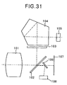
- Fig. 31 is a view illustrating a brief optical configuration of a camera including a conventional focus detection unit.
- reference numeral 101 denotes an object lens which introduces an image of an object (referred as "object image”, hereinafter) into the apparatus;
- 102 a main mirror (half mirror) which is half transparent and reflects a part of light of the object image incoming through the object lens 101;
- 103 a reticle which is placed at a focal plane of the object lens 101;
- 104 a pentagonal prism which changes the traveling direction of light;
- 105 an eyepiece;
- 106 sub-mirror which operates when performing focus state detection;
- 107 a film, such as a silver halide film; and
- 108 a focus state detection unit.
- a part of the light passes through the object lens 101, then a part of the light is reflected by the main mirror 102 upward, and the reflected light forms an image on the reticle 103.
- the image formed on the reticle 103 is further reflected in the pentagonal prism 104 a plurality of times, and eventually reaches the eye of a user through the eyepiece 105. Further, the light which passes through the main mirror 102 reaches the film 107 and exposes it with the object image thereby obtaining a desired image.
- Fig. 32 is a view for explaining the principle of focus state detection in relation to the object lens 101 and the focus state detection unit 108 shown in Fig. 31.
- reference numeral 109 denotes a field stop provided near the desired focal plane, i.e., a conjugate plane of a plane where the film 107 is supplied; 110, a field lens arranged near the desired focal plane; 111, a secondary lens system having two lenses 111-1 and 111-2; 112, a photoelectric conversion device including two line sensors 112-1 and 112-2 provided behind the lenses 111-1 and 111-2, respectively; 113, an iris diaphragm having two aperture openings 113-1 and 113-2 corresponding to the lenses 111-1 and 111-2 of the secondary lens system 111, respectively; and 114, an exit pupil of the object lens 101.
- the field lens 110 has power for forming an image of the aperture openings 113-1 and 113-2 of the iris diaphragm 113 in near areas 114-1 and 114-2 of the exit pupil 114 of the object lens 101.
- fluxes of light 115-1 and 115-2 which passed through the areas 114-1 and 114-2 further pass through the aperture openings 113-1 and 113-2, respectively, and incident on the two line sensors 112-1 and 112-2, thereby distributions of quantity of light are obtained by the two line sensors 112-1 and 112-2.
- the focus state detection unit 108 shown in Fig. 32 adopts a so-called phase-difference detection method.
- the focal point of the object lens 101 is in front of the desired focal plane, namely when an image is focused ahead of the desired focal plane, the images obtained by the two line sensors 112-1 and 112-2 approaches each other.
- the focal point of the object lens 101 is behind the desired focal plane, the images obtained by the two line sensors 112-1 and 112-2 recedes from each other. Since the shifted amount between the distributions of quantity of light of the two line sensors 112-1 and 112-2 has a predetermined functional relationship to a defocus amount of the object lens 101, by calculating the shifted amount between the distributions in accordance with proper operation, it is possible to obtain defocus direction and amount.
- the object lens 101 is moved in accordance with the defocus direction and amount so that the defocus amount approaches 0. When the defocus amount becomes substantially 0, the focus state detection is finished.
- an area used for the focus state detection is a strip and narrow as an area B with respect to an sensed image area A as shown in Fig. 33.
- the size and shape of the detection area B is determined by the shape of the line sensors 112-1 and 112-2, shown in Fig. 32, used in the focus state detection.
- Fig. 34 is a block diagram showing a brief mechanism for charge control of the line sensors 112-1 and 112-2.
- an output VD commonly used as a reference for the line sensors 112-1 and 112-2, of a light-blocked pixel 120 (the pixel is referred as “dark pixel” and the output is referred as "dark voltage”, hereinafter)
- an output VP from a maximum voltage detection circuit 121 connected to the line sensors 112-1 and 112-2 namely the maximum voltage of the line sensors 112-1 and 112-2, are inputted to a differential amplifier 122. Then, the difference between the dark voltage VD and the maximum voltage VP is obtained and outputted.
- Charging of the line sensors 112-1 and 112-2 continues until the difference reaches a predetermined level VR, and when the difference reaches the predetermined level VR, charging of the line sensors 112-1 and 112-2 is terminated and a signal ⁇ R which is an end-charging signal for transferring the stored charges from pixels to charge capacitors is sent to the line sensors 112-1 and 112-2.
- the reason for taking a difference between the maximum voltage VP and the dark voltage VD is that, by charging the line sensors 112-1 and 112-2 until the difference between the maximum voltage VP and the dark voltage VD reaches the predetermined level VR, it is possible to obtain the phase difference between the distributions of quantity of light for focus state detection in sufficient precision.
- Figs. 35A and 35B are graphs showing image signals (distributions of quantity of light) from the line sensors 112-1 and 112-2 with reference to the dark voltage VD of the dark pixel 120, and the maximum voltage VP of first and second images (in Figs. 35A and 35B, the maximum voltage VP is in the first image), corresponding to the line sensors 112-1 and 112-2, respectively, is the predetermined level VR.
- the predetermined level VR For using the signals from the line sensors 112-1 and 112-2 for focus state detection, when the difference between a voltage of any pixel of the line sensors 112-1 and 112-2 and the dark voltage VD reaches the predetermined level VR, charging is terminated and whether or not an image is focused is determined on the basis of output images.
- Fig. 36 is a circuit diagram showing a brief configuration of the maximum voltage detection circuit 121 and its subsequent circuits, namely the differential amplifier 122 and a part of a charge controller 123 both shown in Fig. 34.
- Fig. 36 only two sets of circuits for outputs Vn and Vn-1 outputted from n-th and (n-1)-th pixels, respectively, are connected to a wire 136, however, the same number of similar circuits as that of pixels included in the line sensors 112-1 and 112-2 are actually connected to the wire 136.
- Each pixel output is compared to the current maximum voltage VP, and when an pixel output Vn of the n-th pixel exceeds the current maximum voltage VP, an output from a differential amplifier 130n is reversed and a MOS switch 132n turns ON. Accordingly, the pixel output Vn is outputted through a voltage follower 131n to the wire 136, thereby the pixel output Vn becomes the new maximum voltage VP.
- the maximum voltage VP of the line sensors 112-1 and 112-2 outputted from the maximum voltage detection circuit 121 enters the differential amplifier 122, where the difference between the maximum voltage VP and the dark output VD is obtained and amplified.
- the output from the differential amplifier 122 is compared with the predetermined level VR by a comparator 134, and when the output from the differential amplifier 122 exceeds the predetermined level VR, then the end-charging signal ⁇ R is outputted thereby the charging is terminated. Thereafter, a signal ⁇ RESET is applied to a gate 135 to ground the wire 136, thereby resetting the wire 136 for preparing for the next charge control.
- Fig. 37 shows an example of expanded detection areas B to be used for the focus state detection.
- the detection areas B' in Fig. 37 are obtained by adding three more stripe areas which run in the direction perpendicular to the area B shown in Fig. 33.
- Fig. 38 shows an example of an arrangement of line sensors corresponding to the areas B' shown in Fig. 37.
- a photoelectric conversion element including plural pairs of line sensors C to F (referred as "line sensor pairs”, hereinafter), shown in Fig. 38, and a corresponding lens system (not shown) are provided.
- peripheral circuits such as the one shown in Fig. 34, and a plurality of charge controllers 149 to 152 are provided for respective line sensor pairs C to F in order to control by pair, as shown in Fig. 39.
- differential amplifiers 145 to 148 take differences between dark voltages VD1 to VD4 of the line sensor pairs C to F and maximum voltages VP1 to VP4 outputted from maximum voltage detection circuits 141 to 144, respectively, the differences are compared to the predetermined level VR by charge controller 149 to 152.
- the above is the description of the focus state detection unit using strip sensors, i.e., line sensors.
- the detection area or areas correspond to photo-reception areas of the line sensors, therefore, the shape of the detection area or areas is limited to a line, a plurality of lines, or a combination thereof.
- Fig. 40 shows a detection area B" with respect to the sensed image area A in the focus state detection unit using area sensors.
- the detection area B" is extended greatly compared to the areas B and B' shown in Figs. 33 and 37.
- the photoelectric conversion unit has two two-dimensional photo reception areas, namely, a pair of area sensors (referred as "area sensor pair”, hereinafter) 160-1 and 160-2 as shown in Fig. 41.
- area sensor pair referred as "area sensor pair”, hereinafter
- focus state detection can be performed in two dimensional area.
- a problem due to the number of each detection area is substantially solved if the divided areas are set so as to obtain an arrangement of detection centers as shown in Fig. 42 (i.e., five detection centers in the vertical direction and nine detection centers in the horizontal direction) in the detection area B", namely, in each of area sensors 160-1 and 160-2.
- the photo reception areas are divided in this manner (five divided areas in the vertical direction, as shown in Fig. 43A)
- the number of pixels included in each area is small. It is possible to increase the number of pixels by decreasing the size of each pixel, however, another problem for realizing high efficient photoelectric conversion with narrower aperture openings of down-sized pixels arises.
- the area sensors 160-1 and 160-2 are collectively controlled by a maximum voltage detection circuit 161 (see Fig. 44) using the common dark voltage VD, a differential amplifier 162, and a charge controller 163.
- an image corresponding to an image signal Y, as shown in Fig. 45, used for focus state detection is formed on an area sensor 160-1 or 160-2, and the area sensor 160-1 or 160-2 is divided into four areas, G to J.
- Figs. 46A to 46D are graphs of image signals obtained in the four areas G to J, respectively, which are shown in Fig. 45.
- the area sensors are collectively controlled, charge stored in the area H which includes a pixel charged to the maximum level in the area sensor 160-1 or 160-2 is in ideal level, however, charge stored in the other areas G, I and J are not in ideal levels.
- the detection area is extended, an area to be used for focus state detection is not extended, which wastes an advantage of using area sensors.
- phase-in and phase-out problem variation in focus state detection precision due to a way an image is formed on the line sensors
- the phase-in/phase-out problem is more serious when the object image is formed on the area sensor pair, since the distortion of the object image becomes heavy when it extends in two dimensions.
- the image may be focused on an undesired portion which does not include the object.
- optical members for optically correcting the distortion of the image are required.
- the present invention has been made in consideration of the above situation, and has as one of its concerns to provide a small inexpensive focus state detection apparatus capable of independently controlling each of a plurality of divided areas of area sensors and focusing on an object at an arbitrary position in an image frame at high precision.
- the foregoing object is attained by providing a focus state detection apparatus which detects focus state of an object on the basis of signals obtained from light flux from the object passed through an optical system, the apparatus comprising: a pair of image sensing devices each of which extends in two dimensions and is divided into a plurality of areas each of which is controlled independently; control means for independently controlling charging of each pair of the corresponding divided areas of the pair of image sensing devices; and detection means for detecting focus state on the basis of signals outputted from each pair of divided areas of the pair of image sensing devices after charging of the pair of divided areas is finished under control of the control means.
- a focus state detection apparatus which performs focus state detection on any position in a continuous two-dimensional sensed or observation image, capable of improving unevenness in detected result of focus state, caused by distortion of an object image on the photoelectric conversion devices (so-called phase-in/phase-out problem).
- the foregoing object is attained by providing a focus state detection apparatus which detects focus state of an object on the basis of signals obtained from light flux from the object passed through an optical system, the apparatus comprising: a pair of image sensing devices each of which extends in two dimensions and is divided into a plurality of areas each of which is controlled independently; control means for independently controlling charging of each pair of the corresponding divided areas of the pair of image sensing devices; and detection means for detecting focus state on the basis of signals outputted from each pair of divided areas of the pair of image sensing devices after charging of the pair of divided areas is finished under control of the control means, wherein the pair of image sensing devices are designed so as to compensate for distortion of an image of the object caused by the optical system.
- Fig. 1 is a view showing an optical path for performing focus state detection according to a first embodiment of the present invention
- Fig. 1 is a view showing an optical path for performing focus state detection according to a first embodiment.
- reference numeral 1 denotes the optical axis of an object lens (not shown) provided in the left of Fig. 1; 2, a silver halide film provided at a desired focal plane of the object lens; 3, a main mirror (half mirror) which is half transparent and provided on the optical axis 1; 4, a first mirror provided so as to be tilted on the optical axis 1 of the object lens; 5, an image forming plane of paraxial rays, which is conjugate with the desired focal plane where the film 2 is provided, with respect to the first mirror 4; 6, a second mirror provided for focus state detection; 7, an infrared ray insulating filter for insulating infrared rays; 8, an iris diaphragm having two aperture openings 8-1 and 8-2 as shown in Fig.
- the first mirror 4 has curvature having the power for projecting the two aperture openings 8-1 and 8-2 of the iris diaphragm near the exit pupil of the object lens (not shown). Further, a metal film, such as an aluminum film or silver film, is deposited on the first mirror 4 so that only a necessary area reflects light, therefore, the first mirror 4 functions to mask a field of view for limiting area used for focus state detection. Similarly, metal films are deposited on the other mirrors 6 and 10 in their minimum required areas so as to reduce stray light toward the photoelectric conversion unit 11. It is also effective to paint a light absorbent paint in areas which do not function as reflecting surfaces of the mirrors 4, 6 and 10, or to place shading members near the non-reflecting surface areas of the mirrors 4, 6 and 10.
- Fig. 2 is a plan view of the iris diaphragm 8, and it has the two aperture openings 8-1 and 8-2 arranged so that the long sides of the aperture openings 8-1 and 8-2 are set side by side (in the vertical direction in Fig. 2).
- the portion enclosed by a broken line shows the positions the lenses 9-1 and 9-2 of the secondary lens system 9 provided behind the iris diaphragm 8 in correspondence with the aperture openings 8-1 and 8-2 of the iris diaphragm 8.
- Fig. 3 is a plan view briefly showing the photoelectric conversion unit 11, and each of the two area sensors 11-1 and 11-2, shown in Fig. 1, includes a plurality of pixels arranged in two dimensions as shown in Fig. 3, and is set at a position where an image is formed on the photoelectric conversion unit 11.
- the flux of light 12-1 and 12-2 in Fig. 1 shows the one which forms an image in the central portion of the film 2.
- the first mirror 4 has a curvature of a part of a curved surface obtained by revolving a quadratic curve around an axis, especially, a surface of an ellipsoid of revolution is preferred.
- a surface shape of the first mirror 4 has a curvature of a part of an ellipsoid of revolution obtained by revolving an ellipse 21 whose vertex is a point 20 around an axis 22 of the ellipse 21.
- the primary focal point of the first mirror 4 is set near a point 23 on the axis 22, and the secondary focal point is set near a point (not shown) on an optical axis 24 extended to the left side. Further, the primary focal point is conjugate with the center of the iris diaphragm 8 with respect to the second mirror 6.
- an exit pupil of the object lens is provided. Therefore, an optical image at the exit pupil of the object lens focuses on the primary focal point if not for the second mirror 6.
- the optical image at the exit pupil of the object lens focuses on the center of the iris diaphragm 8 which is at the position conjugate with the primary focal point.
- the first mirror 4 functions as an ideal field lens which focuses the optical image at the exit pupil of the object lens on the center of the iris diaphragm.
- the area of the first mirror 4 corresponds to a portion of the surface of the ellipsoid of revolution which does not include the rotation axis and the vertex.
- Equation (1) shows a quadratic curve.
- k a sphere is obtained when the curve expressed by the equation (1) is rotated; when k is -1, a parabolic is obtained; and when k is greater than -1, an ellipsoid of revolution is obtained.
- h 2 y 2 + z 2 , where x, y and z respectively denote three dimensional axes, and r shows the curvature at the point 20 on the rotation axis 22.
- preferred ranges of r and k are: -20 ⁇ r ⁇ 20 -1 ⁇ k ⁇ -0.2
- the first mirror 4 is put out of the light path of an image when sensing the image, as well as the main mirror 3.
- Fig. 4 is an explanatory view showing a distribution of detection centers seen from a finder via the eyepiece 105 of a camera shown in Fig. 31.
- each small box indicates a detection center of each divided area
- each of the two area sensors 11-1 and 11-2 of the photoelectric conversion unit 11 is divided into 55 areas so that the divided areas corresponds to the respective detection centers.
- each pair of corresponding divided areas of the area sensors 11-1 and 11-2 are called "divided area pair", hereinafter.
- Fig. 5 is an explanatory view showing that each of the area sensors 11-1 and 11-2, shown in Fig. 3, is divided into 55 areas.
- reference numeral 41 denotes dark pixels, corresponding to the dark pixel 120 shown in Fig. 34, for obtaining reference voltages used for obtaining difference between the maximum voltages in each divided area pair of the area sensors 11-1 and 11-2 and the corresponding reference voltage.
- the area sensors are used in the first embodiment, and, since charging is controlled by each divided area pair, one dark pixel is set for each divided area pair.
- the same number of dark pixels as that of the divided area pairs i.e., 55
- a dark pixel is set for each of the 11 ⁇ 5 divided area pairs each of which includes 20 pixels.
- the number of pixels included in each of the 11 ⁇ 5 divided areas is not limited and may be more than 20.
- Fig. 6 is a block diagram illustrating a brief configuration of a charge control unit for the area sensors according to the first embodiment.
- maximum voltage detection circuits 52-1 to 52-n
- differential amplifiers AP 54-1 to 54-n which operate as explained with reference to Fig. 34.
- An output from each of the differential amplifiers AP 54-1 to 54-n enters one terminal of a comparator COM 57 via a corresponding output switch (55-1 to 55-n), and when it reaches a common predetermined level VR, the output from the comparator inverses.
- the reversed output as an end-charging signal ⁇ R instructs the corresponding divided area pair (1 to n) via a corresponding switch (56-1 to 56-n) to end the charging and start reading charges.
- a charge controller 51 sequentially turns “ON" the pairs of switches, 55-1 and 56-1, 55-2 and 56-2, and so on, to 55-n and 55-n, provided for the respective divided area pairs in accordance with a clock signal ICLK.
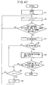
- Fig. 47 is a flowchart showing an operation of the charge control unit.
- step S1 each element of the charge control unit is reset.
- step S2 the count value (i) is increased by 1, and the process proceeds to step S3.
- step S3 whether or not charging a divided area pair corresponding to the count value (i) has been finished in the former routines is determined. If it is, then the process returns to step S2, where the count value (i) is increased by 1, then the subsequent processes are performed.
- step S3 If it is determined in step S3 that the charging the divided area pair corresponding to the count value (i) has not been finished yet, the process proceeds to step S4 and switches 55-i and 56-i are turned ON. Accordingly, the output from the differential amplifier AP 54-i (i.e., the difference between the maximum value VPi at the time when the switches 55-i and 56-i are turned on and the dark voltage VDi, VPi - VDi) is inputted to the comparator COM 57, and compared with the common predetermined level VR.
- the differential amplifier AP 54-i i.e., the difference between the maximum value VPi at the time when the switches 55-i and 56-i are turned on and the dark voltage VDi, VPi - VDi
- step S5 When VPi - VDi is equal or over VR, the end-charging signal ⁇ R is outputted from the comparator COM 57 (YES, in step S5), information indicating that charging the divided area pair i is finished is stored in step S6, then process proceeds to step S7. In step S7, whether or not charging all the divided area pairs is finished or not is checked. If it is, then the processing is completed, whereas, if it is not, the process proceeds to step S8.
- step S5 namely if VPi - VDi of the divided area pair i is less than VR, then the process goes to step S8.
- step S8 whether or not the count value (i) is equal or over the number of the divided area pairs is determined, and if it is not, the process returns to step S2 where the count value (i) is increased by 1 and the subsequent processes are repeated for the next divided area pair. If the count value (i) is equal or over n, then the count value (i) is reset to 0 in step S9, thereafter, the process returns to step S2 and the processes as described above are repeated.
- the charge controller 51 can be configured by a hardware structure or by a software structure using a CPU.
- the control equivalent to the one explained with reference to Fig. 34 is performed for each divided area pair. Therefore, charging operation of two area sensors 11-1 and 11-2 of the photoelectric conversion unit 11 in Fig. 3 is performed in parallel by each divided area pair. Since image signals for focus state detection can be obtained by each divided area pair on the basis of the difference between the maximum value of each divided area pair and the corresponding dark voltage as described above, it is possible to realize high-precision focus state detection.
- phase difference between image signals obtained by each divided area pair occurs in the direction that pixels are arranged in each divided area, namely, in the direction of columns in Fig. 5.
- Fig. 7 is a view showing an arrangement of detection centers when central three columns out of the 11 ⁇ 5 divided areas, shown in Fig. 5, are used for focus state detection.
- control signals to turn on the analog switches 55-i and 56-i corresponding to the desired divided area pairs are sequentially outputted from the charge controller 51.
- circuits corresponding to the fifteen divided area pairs are selected to operate. For example, in a case where the detection centers shown in Fig. 4 are numbered sequentially from the upper-right corner (top-down and to the left), the switches 55-21, 56-21 to 55-35 to 56-35 corresponding to the twenty-first to twenty-fifth detection centers as shown in Fig. 7 are sequentially turned ON.
- the purpose of limiting the number of the divided area pairs to be used for focus state detection is to avoid inappropriate charged state when sensing a high-luminous object, i.e., saturated state. More specifically, since the charge control in the first embodiment is performed sequentially by each divided area pair, determination on timing for terminating charging a given divided area pair is performed at certain interval. If a period of time for obtaining proper image signals by charging the given divided area pair is short, only the saturated image signals may be obtained when timing for terminating charging all the divided area pairs are sequentially determined as described above with reference to Fig. 47. In such case, it is impossible to detect focus state. Thus, by reducing the number of the divided area pairs to be charge controlled, the interval at which the determination on charged state of each divided area pair is shortened, thereby proper charging may be performed.
- the limitation on the number of divided area pairs is set by unit of column (five divided area pairs in the vertical direction) in the sensed image area 31. This is to restrain the size of the charge controller 51 while providing it with necessary function for controlling each divided area pair. Even without providing an ability for limiting arbitrary divided area pairs to the charge controller 51, with control for prohibiting divided area pairs to output signals, which is explained in the following embodiments, selection of arbitrary divided area pairs to be used for focus state detection can be realized.
- Fig. 8 is a view showing five horizontal units 61 to 65 of detection centers by which transference of charges are restricted in the sensed image area 31.
- a signal to control to end charging is outputted to all the divided area pairs which belongs to a horizontal unit simultaneously.
- Fig. 9 is a circuit diagram for explaining output restriction function according to the third embodiment.
- an output terminal INTE for outputting the end-charging signal ⁇ R is connected to a microcomputer which controls the overall operation of the camera so that the microcomputer can detect the completion of charging operation.
- the INTE terminal is provided in order to notify the microcomputer of completion of charging any of divided area pair in a horizontal unit. Charge output is allowed or prohibited by each of five horizontal units 61 to 65 shown in Fig. 8.
- end-charging signals END1 to END55 (corresponding to ⁇ R signal for each divided area pair.
- the numbers indicate the respective divided area pairs when the detection centers, shown in Fig. 8, are numbered sequentially from the upper-right corner (top-down and to the left) are inputted to OR gates 71-1 to 71-5 corresponding to the horizontal units 61 to 65, respectively, by horizontal unit, then outputs from the OR gates 71-1 to 71-5 enter respective AND gates 72-1 to 72-5.
- Control signals INH1 to INH5 are also inputted to the AND gates 72-1 to 72-5 via inverters 73-1 to 73-5.
- Outputs from the AND gates 72-1 to 72-5 are inputted to an OR gate 74, and the output from the OR gate 74 is outputted to the INTE terminal.
- the control signals INH1 to INH5 are used for controlling the respective horizontal units 61 to 65.
- the detection of completion of charging only the divided area pairs to be actually used for focus state detection is needed, excess individual control of divided area pairs is not necessary.
- control signals INH1 and INH2 are set to "0" so as to select the upper two horizontal lines, and the remaining control signals INH3 to INH5 are set to "1". Accordingly, charge output from the divided area pairs belonging to the horizontal units 61 and 62 is allowed. Accordingly, when maximum voltages with respect to corresponding dark voltages in divided area pairs which do not belong to the selected two horizontal units exceed the predetermined level VR, charging operation is continued and charges are not outputted from those divided area pairs.
- Fig. 10 shows an example for controlling the divided area pairs by combining the limitation on the number of divided area pairs to be used for focus state detection by column as described in the second embodiment with reference to Fig. 7 and the output restriction explained with reference to Figs. 8 and 9 when the control signals INH1 and INH5 are set to "1", so that image signals are outputted only from the divided area pairs corresponding to the nine central detection centers.
- the same effect as operating only the central nine divided area pairs can be achieved.
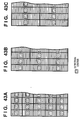
- Fig. 11 is a view showing a distribution of detection centers according to a fifth embodiment of the present invention.
- limitation on divided area pairs to be used for focus state detection is applied to discrete columns, and output restriction is applied to four horizontal lines (in this case, INH3 in Fig. 9 is "0" and other control signals are "1").
- INH3 in Fig. 9 is "0" and other control signals are "1".
- Fig. 12 is a view showing a distribution of detection centers according to the fifth embodiment of the present invention. Referring to Fig. 12, only one column is selected and the output restriction is performed except one horizontal line. In this case, a control for virtually operating only one divided area pair is realized. More specifically, when completion of charging this divided area pair is detected, charged signals stored only in this divided area pair are outputted.
- Fig. 13 shows a distribution of detection centers seen from a finder of a camera according to a sixth embodiment of the present invention. As shown in Fig. 13, in the central part of the sensed image area 31, three detection centers and two detection centers are alternatively provided in columns. Each of the area sensors 11-1 and 11-2 is divided into 27 areas so as to correspond to detection centers arranged as described above in a check pattern.
- a detection center should be arranged, basically. Therefore, according to the sixth embodiment, the odd number (three and five) of detection centers are set in the column and row including the center of the sensed image area (shown by a square with oblique lines in Fig. 14), and detection centers are arranged symmetrically with respect to both the vertical and horizontal lines passing through the center of the sensed image area 31, as shown in Fig. 14, to give balanced-looking and increase operability.
- each area sensor is divided so that density of detection centers in the horizontal direction is relatively high, whereas density of detection centers in the vertical direction is relatively low. More specifically, referring to Fig. 14, as for the intervals, h and v, between detection centers in the horizontal and vertical directions, relationship h ⁇ v is set. In this relationship, the interval between the detection centers is shorter in the direction of the long side of the sensed image area than that in the direction of the short side and the more the detection centers are arranged in the direction of the long side than those arranged in the short side. With the aforesaid arrangement, the detection centers are distributed densely in the two dimensional area.
- h ⁇ v
- v ⁇ 2h
- 2h is the horizontal interval between detection centers which are in columns including the same number of detection centers (namely, columns including three detection centers or columns including two detection centers, in this case).
- Each of the area sensors 11-1 and 11-2 of the photoelectric conversion unit 11 is divided into 27 areas corresponding to respective detection centers as described above.
- Fig. 15 is a view showing a plurality of divided areas of one of the area sensors according to the sixth embodiment. As seen in Fig. 15, by dividing the sensor having the limited number of pixels are divided into three or two areas in the vertical direction, it is possible to achieve good precision in focus state detection since the enough number of pixels are included in each area.
- each area sensor is divided into 27 areas
- the number of n is 27 in the sixth embodiment.
- the sixth embodiment is not limited to this.
- two more columns, one divided into three areas and the other divided into two areas may be added to the 27 divided areas in each of the right and left sides to obtain 37 divided areas.
- two columns, i.e., five divided areas may be cut from each of the right and left sides of the 27 divided areas to obtain 17 divided areas.
- the columns may be divided into three and four areas.
- intervals between the detection centers are intentionally made different in the vertical direction from the horizontal direction.
- a camera is sometimes used to take a photo with the shorter side at the top, in which case, the conceptions of "vertical” and “horizontal” are exchanged.
- intervals between the detection centers in the vertical and horizontal directions are made equal.
- Fig. 17 shows an example of the detection centers arranged as described above. As seen in Fig. 17, the detection centers are arranged so that the intervals between detection centers in the vertical and horizontal direction are set on the basis of the ratio of one side length to the other side length of the sensed image area. More specifically, as shown in Fig. 18, the relationship between h and v is the same as the relationship between the horizontal side length and the vertical side length of the sensed image area. Inversely, the sensed image area may be designed so as to optimize the relationship between h and v.
- the detection centers so that the ratio of the number of the detection centers in the horizontal direction to the number in the vertical direction equals to the ratio of the horizontal side length to the vertical side length of the sensed image area.
- distributions of quantity of light are obtained by the area sensors 11-1 and 11-2, which are arranged separately in the vertical direction, of the photoelectric conversion unit 11, as shown in Fig. 3, and the shift between the distributions in the vertical direction is detected.
- a focus state detection apparatus having this type of configuration, it is possible to focus on an object whose luminance varies in the vertical direction, e.g., an object having horizontal stripes, however, it is not possible to focus on an object whose luminance does not vary in the vertical direction, e.g., an object having vertical stripes.
- FIG. 19 An arrangement of optical system according to an eighth embodiment addressed to overcome the aforesaid problem is shown in Fig. 19.
- Difference between the configurations shown in Fig. 19 and shown in Fig. 1 is that, in Fig. 19, two more lenses 9-3 and 9-4 are added to the secondary lens system 9 in the orthogonal direction with respect to the two lenses 9-1 and 9-2, and aperture openings 8-3 and 8-4 of the iris diaphragm 8 and area sensors 11-3 and 11-4 of the photoelectric conversion unit 11 are provided so as to correspond to the lenses 9-3 and 9-4.
- the aperture openings 8-1 and 8-2 of the iris diaphragm 8, the area sensors 11-1 and 11-2 of the photoelectric conversion unit 11, and the light flux 12-1 and 12-2, illustrated in Fig. 1, are not shown in Fig. 19.
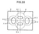
- Fig. 20 shows shapes of the aperture openings of the iris diaphragm 8 according to the eighth embodiment.
- reference numerals 8-3 and 8-4 indicate the added aperture openings (shown by solid lines), and 9-3 and 9-4 indicate two lenses (shown by broken lines) configuring a part of the secondary lens system 9 provided in correspondence to the aperture openings 8-3 and 8-4 and arranged behind them.
- the aperture openings 8-3 and 8-4 are set at a distance farther than the distance from the center of the iris diaphragm 8 to the aperture openings 8-1 and 8-2 so as to collect light passing through the periphery of the pupil of the object lens (not shown).
- the length of, so-called, a base line can be extended upon focus state detection.
- the optical system, corresponding to the aperture openings 8-3 and 8-4 of the iris diaphragm 8, newly added in the eighth embodiment increases precision of the focus state detection when a bright lens (i.e., a lens having small f-number) is used as the object lens.
- the aperture openings 8-3 and 8-4 of the iris diaphragm 8 may be arranged at the same distance as the aperture openings 8-1 and 8-2 from the center of the iris diaphragm 8.
- Fig. 21 shows an arrangement of the area sensors 11-3 and 11-4, corresponding to the lenses 9-3 and 9-4, of the photoelectric conversion unit 11 for obtaining distributions of quantity of light.
- the visual fields corresponding to the area sensors 11-3 and 11-4 for detecting phase differences between images in the horizontal direction are set smaller than the visual fields of the area sensors 11-1 and 11-2 for detecting phase differences between images in the vertical direction.
- the reason for setting the sizes of the area sensors 11-1 to 11-4 small is to realize a secondary lens system causing less distortion of an image both in the vertical and horizontal directions and avoid increase in size of the photoelectric conversion unit.
- Charging control of the four area sensors 11-1 to 11-4 is performed by each divided area pair of the area sensors 11-1 and 11-2, and of the area sensors 11-3 and 11-4 on the basis of the maximum voltage in each divided area pair.
- charge control for the plural pairs of line sensors described with reference to in Fig. 38 is applied to the plural pairs of area sensors, and by detecting the maximum voltage in each divided area pair of the corresponding area sensors and obtaining the end-charging signal for each divided area pair, it is possible to obtain signals of proper level for focus state detection from the broad image sensing area.
- incoming light passing through the object lens is separated into two images having a parallax, then respective two separated images are formed on the respective area sensors, however, the present invention is not limited to this.
- two images of an object incoming through two lenses separated at a predetermined base-line distance may be formed on the respective area sensors.
- the focus state detection apparatus capable of performing focus state detection in a broad area of a continuous two-dimensional image sensing area or observation area
- signals of proper-level are obtained by each of a plurality of divided area pairs of a plurality of photoelectric conversion devices, as photoreceptors, which extend continuously in two dimensions, and charge control is performed independently for the respective divided areas. Accordingly, it is possible to focus on an object whose image is formed on any position in the area of two-dimensional photoelectric conversion devices easily and at high precision.
- the size of the control circuit is reduced, thereby a focus state detection apparatus can be provided at low price.
- Fig. 22 shows a case where each of the area sensors 11-1 and 11-2, shown in Fig. 3, is configured with a conventional area sensor.
- Reference numeral 93-1 denotes photoelectric conversion pixel array arranged in two dimension
- reference numeral 93-2 denotes a distorted image formed on the photoelectric conversion pixel array 93-1.
- the photoelectric conversion pixel array 93-1 has a flat rectangular shape, and pixels having a rectangular shape are arranged in the vertical and horizontal directions.
- the image 93-2 is distorted in a barrel shape while passing through the lens system.
- Fig. 23 is a view for explaining the phase-in/phase-out on the photoelectric conversion pixel array.
- reference numeral 90-1 denotes each pixel of the photoelectric conversion pixel array 93-1
- reference numeral 90-2 denotes a portion of an image formed on the photoelectric conversion pixel array 93-1.
- Fig. 25 is a graph showing a variation in precision of focus state detection caused by the phase-in/phase-out of the image formed on the photoelectric conversion pixel array 93-1.
- the abscissa shows the position of the image portion 90-2 when it is moved in the direction of an arrow shown in Fig. 23 and the ordinate shows a defocus amount.
- the defocus amount caused by phase-in/phase-out of the image on the photoelectric conversion pixel array alters with a spatial period corresponding to the pixel-width of the photoelectric conversion pixel array.
- pixels are conventionally arranged as shown in Fig. 24.
- Fig. 24 a line of photoelectric conversion pixels a to g and another line of photoelectric conversion pixels h to n are shifted by 1/2 pixel.
- the detected result of defocus amount using these photoelectric conversion pixel lines is shown in Fig. 26.
- Fig. 26 In this configuration, in addition to the defocus amount 96-1 obtained on the basis of the output from the photoelectric conversion pixels a to g expressed with a solid line which is the same as the defocus amount shown in Fig.
- the defocus amount 96-2 is obtained on the basis of the output from the photoelectric conversion pixels h to n shown by a dotted line. By simply adding these defocus amounts at each position, the total defocus amounts becomes 0 (96-3), as shown by the line 96-3.
- the photoelectric conversion pixel lines are shifted by a predetermined amount and a single defocused amount is obtained by adding defocused amounts obtained on the basis of outputs from pixels in adjoining two lines, it is confirmed theoretically and experimentally that, when the adjoining photoelectric conversion pixel lines are shifted by 1/2 pixels, the best result is obtained.
- FIG. 27 The photoelectric conversion unit for overcoming the above problem is shown in Fig. 27, and a portion of the photoelectric conversion unit is shown in Fig. 28.
- reference numeral 94-1 denotes each photoelectric conversion pixel, and 94-2, a distorted image formed on the photoelectric conversion pixels.
- Fig. 29 shows the photoelectric conversion pixel lines which is an magnified view of the photoelectric conversion unit shown in Fig. 28. Referring to Fig. 29, photoelectric conversion pixel lines 97-1 and 97-2 are arranged so that the photoelectric conversion pixel lines 97-1 and 97-2 are shifted by 1/2 pixel with respect to an image 97-3 of the object expressed with oblique lines.
- phase difference between the photoelectric conversion pixel lines 97-1 and 97-2 is 1/2 pixel with respect to the image 97-3 even through the image 97-3 is distorted.
- the feature of the photoelectric conversion unit arranged as described above comparing to the arrangement shown in Fig. 24 is that the photoelectric conversion unit of the present invention has a plurality of pixel lines arranged so as to compensate for the distortion of the image of the object, and the phase of one line and the phase of the next line is shifted by 1/2 pixel with respect to the light flux from the object.
- neighboring photoelectric conversion pixel lines are arranged so that they are shifted by a predetermined amount (1/2 pixel in the ninth embodiment) with respect to the light flux from the object, and one defocus amount is obtained on the basis of two defocus amounts obtained on the basis of outputs from the neighboring photoelectric conversion pixel lines. Accordingly, even when the image sensing area to be used for focus state detection is broadened, it is possible to always perform stable focus state detection by preventing effects of a variation in defocus amount due to phase-in/phase-out problem.
- the area sensors 11'-1 and 11'-2 may be divided as described in the sixth and seventh embodiments, or into other pattern. It is also possible to add the configuration as described in the eighth embodiment.
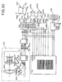
- Fig. 30 is a diagram illustrating a brief configuration of a camera including a focus state detection apparatus which is as described above.
- reference PRS denotes a control unit which is, for instance, an one-chip microcomputer having a CPU 301, ROM 302, RAM 303, an analog-digital converter 304, and a digital-analog converter 305.
- the microcomputer PRS controls overall operation of the camera, such as automatic exposure control, automatic focusing adjustment, film advancing, film rewinding, etc., in accordance with sequence programs stored in the ROM 302.
- the microcomputer PRS communicates with inside circuits of the camera and a lens control unit by using communication signals SO, SI and SCLK, and communication selection signals CLCM, CDDR and CICC, to control operation of each circuit and lens.
- SO is a data signal outputted from the microcomputer PRS
- SI is a data signal inputted to the microcomputer PRS
- SCLK is a synchronizing clock for signals SO and SI.
- reference LCM denotes a lens communication buffer circuit, and it supplies electric power to a power input terminal VL for lens when the camera is under operation, further, when the selection signal CLCM from the microcomputer PRS is in high potential level (referred as "H”, and low potential level is referred as “L”, hereinafter), it acts as a communication buffer between the microcomputer PRS and the lens.
- H high potential level
- L low potential level
- the lens communication buffer circuit LCM When the microcomputer PRS controls the selection signal CLCM to be "H” and outputs predetermined data from as the data signal SO in synchronization with the synchronizing clock SCLK, the lens communication buffer circuit LCM outputs buffer signals LCK and DCL corresponding to the synchronizing clock SCLK and the data signal LO, respectively, to the lens via a communication node between the microcomputer PRS and the lens.
- a buffer signal of the signal DLC is outputted from a lens unit LNS as the data signal SI, and the microcomputer PRS receives data of the lens as the data signal SI in synchronization with the synchronizing clock SCLK.
- Reference DDR denotes a circuit for detecting operation of various switches SWS and for display. It is selected when the signal CDDR is "H", and controlled by the microcomputer PRS by using the data signals SO and SI, and the synchronizing clock SCLK. More specifically, the circuit DDR changes displayed contents on a display member DSP of the camera on the basis of data sent from the microcomputer PRS, and notifies the microcomputer PRS of the ON/OFF state of each of the operation switches SWS of the camera by communication.
- Reference OLC denotes an outside liquid crystal display provided in the upper portion of the camera
- reference ILC denotes a liquid crystal display inside of a finder. In the tenth embodiment, settings of an area used for the focus state detection is performed using the switches SWS connected to the circuit DDR for detection and display.
- Switches SW1 and SW2 are coupled with a release button (not shown), and with a half press of the release button, the switch SW1 is turned on, and with a full press of the release button, the switch SW2 is turned on.
- the microcomputer PRS performs photometry and automatic focusing adjustment in response to the "on" operation'of the switch SW1, and in response to the "on” operation of the switch SW2, it controls exposure, thereafter, advances the film a frame.
- the switch SW2 is connected to an interruption input terminal of the microcomputer PRS, and even when programs triggered by the "on” operation of the switch SW1 is under execution, the "on” operation of the switch SW2 interrupts the execution, and the microcomputer PRS swiftly moves to a predetermined interrupt program.
- Reference MTR1 denotes a motor-for advancing the film
- reference MTR2 denotes a motor for moving a mirror in the up and down direction and charging of a shutter spring, and the film and the mirror are controlled to move in the forward and reverse directions by the motors MDR1 and MDR2, respectively.
- Signals M1F, M1R, M2F and M2R, inputted from the microcomputer PRS to driving circuits MDR1 and MDR2, are forward and reverse rotation control signals.
- References MG1 and MG2 denote front and rear shutter operation magnet, which is supplied with electric power via amplifying transistors TR1 and TR2 in response to control signals SMG1 and SMG2, and the shutter is controlled by the microcomputer PRS.
- a buffer signal DCL which is inputted to the control circuit LPRS inside of the lens unit LNS in synchronization with the buffer signal LCK is instruction data from the microcomputer PRS to the lens unit LNS, and operation of the lens unit LNS corresponding to each instruction is predetermined.
- the control circuit LPRS inside of the lens unit LNS analyzes the instruction in a predetermined procedure, and outputs operation states of focusing control, iris diaphragm control, the output signal DLC, each element of the lens unit LNS (e.g., operation states of focusing control optical system and operation states of iris diaphragm), and various parameters (open f-number, focus distance, coefficient of amount of movement of focusing control optical system corresponding to defocus amount, various focus correction amounts, etc.)
- a zoom lens is explained in the tenth embodiment as an example, and when an instruction of focusing adjustment is transmitted from the microcomputer PRS, a motor LMTR for focusing adjustment is operated on the basis of the signals LMF and LMR showing an amount and direction of displacement which are transmitted simultaneously. Accordingly, focusing adjustment is performed by either rotating the optical system in the forward or reverse direction along the optical axis. The amount of displacement of the optical system is obtained in the following manner.
- a pattern of a pulse board, which rotates, coupled with the optical system, is detected by a photocoupler, monitoring a pulse signal SENCF outputted from an encoder ENCF which outputs pulses whose number corresponds to the displacement amount, and the number of the pulses is counted by a counter provided inside of the control circuit LPRS inside of the lens unit LNS.
- the control circuit LPRS inside of the lens unit LNS controls the signals LMF and LMR to "L" to operate the motor LMTR.
- the microcomputer PRS does not care about operation of the lens until the lens finishes displaced. Further, the control circuit LPRS transmits the value of the counter to the microcomputer PRS when the microcomputer PRS requests to do so.
- a stepping motor DMTR which is known for driving an iris diaphragm is operated based on an iris diaphragm stage number transmitted at the same time. Note, since the stepping motor DMTR can control to open the iris diaphragm, an encoder for monitoring the operation is not necessary.
- Reference ENCZ denotes an encoder attached to a zoom optical system
- the control circuit LPRS inside of the lens unit LNS detects the zoom position by receiving a signal SENCZ from the encoder ENCZ.
- the control circuit LPRS inside of the lens unit LNS stores lens parameters corresponding to respective zoom positions, and outputs a parameter corresponding to a current zoom position to the microcomputer PRS when the microcomputer PRS requests to do so.
- Reference ICC denotes a focus state detection circuit, including area sensors, configured with CCDs which are photoelectric converters, etc., used for focus state detection and their operation control circuit.
- the focus state detection circuit ICC is selected when the selection signal CICC is "H", and controlled by the microcomputer PRS using the data signals SO and SI, and the synchronizing clock SCLK.
- ⁇ V and ⁇ H are read signals for the area sensors, and ⁇ R is a reset signal.
- These sensor signals are generated by a driving circuit provided inside of the focus state detection circuit ICC on the basis of signals from the microcomputer PRS.
- the signals outputted from the area sensors are amplified, then inputted into an analog signal input terminal of the microcomputer PRS as output signals IMAGE. Thereafter, the microcomputer PRS converts the analog output signals IMAGE into digital signals, and the values of the digital signals are sequentially stored in the RAM at predetermined addresses. With these digitized signals, the focus state detection is performed.
- Reference VR denotes a predetermined level, explained in the first embodiment, used for detecting timing for terminating charging operation and is common for all the differential amplifiers; INTE, a terminal for outputting an end-charging signal; and ICLK, a reference clock signal for the control circuits inside of the focus state detection circuit ICC.
- the focus state detection circuit ICC performs focus state detection by using area sensors, as described in the first to ninth embodiments, and the detected result is used in the control circuit LPRS inside of the lens unit LNS via the microcomputer PRS to move and fix the optical system to focus on a desired point. Thereafter, with the operation of the shutter button, a focused image can be photographed.
- the camera and lens unit LNS are separable (i.e., lens can be exchanged), however, the present invention is not limited to this, and the camera and lens may be configured integrally.
Landscapes
- Physics & Mathematics (AREA)
- General Physics & Mathematics (AREA)
- Optics & Photonics (AREA)
- Focusing (AREA)
- Automatic Focus Adjustment (AREA)
Abstract
Description
Claims (42)
- A focus state detection apparatus which detects focus state of an object on the basis of signals obtained from light flux from the object passed through an optical system (Figs. 1 and 19), said apparatus characterized by comprising:a pair of image sensing devices (11-1, 11-2, 11'-1, 11'-2) each of which extends in two dimensions and is divided into a plurality of areas (Fig. 5, Fig. 15) each of which is controlled independently;control means (Fig. 6, PRS) for independently controlling charging of each pair of the corresponding divided areas of said pair of image sensing devices; anddetection means (PRS) for detecting focus state on the basis of signals outputted from each pair of divided areas of said pair of image sensing devices after charging of the pair of divided areas is finished under control of said control means.
- The focus state detection apparatus according to claim 1, wherein said focus state detection apparatus detects focus state by phase-difference detection method, and said pair of image sensing devices (11-1, 11-2, 11'-1, 11'-2) are arranged side by side in the direction that phases of the signals outputted from each pair of divided areas of said pair of image sensing devices are shifted, and said pair of image sensing devices are divided into a plurality of strips (Figs. 5 and 15) in the direction that the phases are shifted.
- The focus state detection apparatus according to claim 1, wherein said pair of image sensing devices (11-1, 11-2, 11'-1, 11'-2) includes a plurality of rectangular pixels, and said pair of image sensing devices are divided into a plurality of strips (Figs. 5 and 15) along the shorter side of the rectangular pixels.
- The focus state detection apparatus according to claim 2, wherein each of the plurality strips is further divided in the direction perpendicular to the direction of the strips (Figs. 5 and 15).
- The focus state detection apparatus according to claim 4, wherein each of the plurality of strips is further divided in the direction perpendicular to the direction of the strips so that central portions of respective divided areas are arranged in a check pattern (Fig. 15).
- The focus state detection apparatus according to claim 5, wherein one of the central portions is set on an optical axis of the optical system (Fig. 16).
- The focus state detection apparatus according to claim 5, wherein the central portions are arranged symmetrical with respect to top-to-bottom and right-to-left lines which intersect with the optical axis of the optical system (Figs. 16 to 18).
- The focus state detection apparatus according to claim 5, wherein the central portions are arranged at different intervals in the top-to-bottom direction from the right-to-left direction (Figs. 14, 16, 18).
- The focus state detection apparatus according to claim 8, wherein the interval between the central portions in the top-to-bottom direction is wider than the interval between the central portions in the right-to-left direction (Figs. 14, 16, 18).
- The focus state detection apparatus according to claim 8, wherein, the central portions are arranged at wider interval in one direction, in which phases of the signals outputted from each pair of divided areas of said pair of image sensing devices are shifted in a case where focus state is detected by performing phase-difference detection method, than the other direction.
- The focus state detection apparatus according to claim 8, wherein the interval between the central portions in one direction is less than twice the interval between the central portions in the other direction (Fig. 14).
- The focus state detection apparatus according to claim 8, wherein a ratio of a number of the central portions in the top-to-bottom direction to a number of the central portions in the right-to-left direction is the same as a ratio of a length of top-to-bottom side to a length of right-to-left side of an image.
- The focus state detection apparatus according to claim 8, wherein relationship between the interval of the central portions in the top-to-bottom direction and the interval of the central portions in the right-to-left direction is the same as relationship between a length of top-to-bottom side and a length of right-to-left side of an image.
- The focus state detection apparatus according to claim 8, wherein the intervals between the central portions in the top-to-bottom direction and in the right-to-left direction are the same.
- The focus state detection apparatus according to claim 1, wherein said control means (Fig. 6) individually controls to stop charging all the pixels in each pair of divided areas on the basis of a maximum charge amount in the pair of divided areas.
- The focus state detection apparatus according to claim 15, wherein said pair of image sensing devices includes a plurality of reference signal output units (41) for outputting reference signals for the respective pair of divided areas, and said control means (Fig. 6) has a judgment means (54-1 to 54-n, 57) for comparing a difference between the maximum charge amount in each pair of divided areas and the reference signal outputted from said corresponding reference signal output unit, to a predetermined value, and judging whether or not the difference is equal or greater than the predetermined value.
- The focus state detection apparatus according to claim 16, wherein said control means (Fig. 6) further comprises the same number of maximum value detection circuits (52-1 to 52-n) as the pairs of divided areas for detecting the maximum charge amounts in the respective pairs of divided areas, and said judgment means (54-1 to 54-n, 57) has the same number of differential amplifier (54-1 to 54-n) as the pairs of divided areas for detecting differences between the maximum charge amounts of the respective pairs of divided areas outputted from said maximum value detection circuits and the corresponding reference signals (VD1 to VDn), and comparison means for sequentially comparing the differences detected by said differential amplifiers to the predetermined value.
- The focus state detection apparatus according to claim 16, wherein, when said judgment means (54-1 to 54-n, 57) judges that the difference between the maximum charge amount in one of the pairs of divided areas and the corresponding reference signal is equal or greater than the predetermined value, said control means (Fig. 6) controls to stop charging the pair of divided areas.
- The focus state detection apparatus according to claim 18, wherein said judgment means (54-1 to 54-n, 57) performs judgment on a pair or pairs of divided areas selected in advance.
- The focus state detection apparatus according to claim 19, wherein said focus state detection apparatus detects focus state by performing phase-difference detection method, said pairs of image sensing devices (11-1, 11-2, 11'-1, 11'-2) are arranged side by side in the direction in which phases of the signals outputted from each pair of divided areas of said pair of image sensing devices are shifted, and said pair of image sensing devices are divided into a plurality of strips in the direction in which the phases are shifted, and the pair or pairs of divided areas selected in advance is the pair or pairs of strips.
- The focus state detection apparatus according to claim 16, wherein said control means (Figs. 6, 9) prohibits a plurality of predetermined pairs of divided areas to output signals (Figs. 10, 11, 12).
- The focus state detection apparatus according to claim 21, wherein the predetermined pairs of divided areas are set by row in the right-to-left direction.
- The focus state detection apparatus according to claim 1, wherein said control means (Fig. 6) sequentially determines time for stopping charging the pairs of divided areas.
- The focus state detection apparatus according to claim 2 further comprising a pair of image sensing devices (11-3, 11-4) each of which extends in two dimensions and divided into a plurality of areas in the direction perpendicular to the strips.
- The focus state detection apparatus according to claim 1, wherein said pair of image sensing devices (11'-1, 11'-2) are designed so as to compensate for distortion of an image of the object caused by the optical system.
- The focus state detection apparatus according to claim 25, wherein said focus state detection apparatus detects focus state by phase-difference detection method, and said pair of image sensing devices (11'-1, 11'-2) are arranged side by side in the direction that phases of the signals outputted from each pair of divided areas of said pair of image sensing devices are shifted, and have pixel arrays arranged in a stripe pattern in the direction which phases are shifted, and each pixels array is shifted from adjoining pixel arrays by one half pixel in the direction which the phases are shifted with respect to the image of the object (Fig. 29).
- The focus state detection apparatus according to claim 25, wherein said pair of image sensing devices (11'-1, 11'-2) includes a plurality of pixel arrays whose pixels have a rectangular shape arranged in a stripe pattern, and each of pixel arrays is shifted from adjoining pixel arrays by one half pixel in the direction where the phases are shifted along the shorter side of the rectangular pixels (Fig. 29).
- An image sensing apparatus including a focus state detection apparatus which detects focus state of an object on the basis of signals obtained from light flux from the object passed through an optical system (Figs. 1 and 19), said apparatus characterized by comprising:a pair of image sensing devices (11-1, 11-2, 11'-1, 11'-2) each of which extends in two dimensions and is divided into a plurality of areas (Fig. 5, Fig. 15) each of which is controlled independently;control means (Fig. 6, PRS) for independently controlling charging of each pair of the corresponding divided areas of said pair of image sensing devices; anddetection means (PRS) for detecting focus state on the basis of signals outputted from each pair of divided areas of said pair of image sensing devices after charging of the pair of divided areas is finished under control of said control means.
- The image sensing apparatus according to claim 28, wherein said control means (Fig. 6) individually controls to stop charging all the pixels in each pair of divided areas on the basis of a maximum charge amount in the pair of divided areas.
- The image sensing apparatus according to claim 28, wherein said control means (Figs. 6, 9) prohibits a plurality of predetermined pairs of divided areas to output signals (Figs. 10, 11, 12).
- The image sensing apparatus according to claim 28, wherein said pair of image sensing devices (11'-1, 11'-2) are designed so as to compensate for distortion of an image of the object caused by the optical system.
- A photoelectric conversion apparatus characterized by comprising:image sensing device (11-1, 11-2, 11'-1, 11'-2) which extends in two dimensions and is divided into a plurality of areas (Fig. 5, Fig. 15) each of which is controlled independently; andcontrol means (Fig. 6, PRS) for independently controlling charging of the divided areas.
- The photoelectric conversion apparatus according to claim 32, wherein said control means (Fig. 6) individually controls to stop charging all the pixels in each divided area on the basis of a maximum charge amount in the divided area.
- The photoelectric conversion apparatus according to claim 33, wherein said image sensing device includes a plurality of reference signal output units (41) for outputting reference signals for the respective divided areas, and, when the difference between a maximum charge amount in one of the divided areas and the corresponding reference signal is equal or greater than a predetermined value, said control means (Fig. 6) controls to stop charging the divided area.
- The photoelectric conversion apparatus according to claim 34, wherein said control means (Figs. 6, 9) prohibits a plurality of predetermined divided areas to output signals (Figs. 10, 11, 12).
- The photoelectric conversion apparatus according to claim 35, wherein the predetermined divided areas are set by row in the right-to-left direction.
- The photoelectric conversion apparatus according to claim 32, wherein said control means (Fig. 6) sequentially determines time for stopping charging the divided areas.
- The photoelectric conversion apparatus according to claim 32, wherein said image sensing device (11'-1, 11'-2) are designed so as to compensate for distortion of an image of the object caused by the optical system.
- The photoelectric conversion apparatus according to claim 38, wherein said image sensing device (11'-1, 11'-2) includes a plurality of pixel arrays whose pixels have a rectangular shape arranged in a stripe pattern, and each of pixel arrays is shifted from adjoining pixel arrays by one half pixel in the direction where the phases are shifted along the shorter side of the rectangular pixels (Fig. 29).
- A focus state detection apparatus which detects the focus state of an object on the basis of light from the object passed through an optical system, wherein:each one of a pair of two-dimensional image sensing devices (11-1, 11-2, 11'-1, 11'-2) is divided into a plurality of areas, with each areas on a first one of the image sensing devices corresponding to an area on the other image sensing device;control means (PRS) independently controls the charging of each corresponding area pair; anddetection means (PRS) detects the focus state on the basis of signals emitted from each corresponding area pair after charging of the area pair.
- An image sensing apparatus including the focus state detection apparatus of claim 40.
- A photoelectric conversion apparatus including the focus state detector of claim 40.
Applications Claiming Priority (9)
| Application Number | Priority Date | Filing Date | Title |
|---|---|---|---|
| JP25628896A JP3789012B2 (en) | 1996-09-27 | 1996-09-27 | Photoelectric conversion device, imaging device, and focus detection device using the same |
| JP256288/96 | 1996-09-27 | ||
| JP25628896 | 1996-09-27 | ||
| JP256290/96 | 1996-09-27 | ||
| JP25629096 | 1996-09-27 | ||
| JP25628996A JP3684001B2 (en) | 1996-09-27 | 1996-09-27 | Focus detection device |
| JP25629096A JP3696989B2 (en) | 1996-09-27 | 1996-09-27 | Focus detection device and camera using the same |
| JP25628996 | 1996-09-27 | ||
| JP256289/96 | 1996-09-27 |
Publications (3)
| Publication Number | Publication Date |
|---|---|
| EP0834757A2 true EP0834757A2 (en) | 1998-04-08 |
| EP0834757A3 EP0834757A3 (en) | 1999-04-28 |
| EP0834757B1 EP0834757B1 (en) | 2005-04-06 |
Family
ID=27334516
Family Applications (1)
| Application Number | Title | Priority Date | Filing Date |
|---|---|---|---|
| EP97307561A Expired - Lifetime EP0834757B1 (en) | 1996-09-27 | 1997-09-26 | Photoelectric conversion apparatus |
Country Status (3)
| Country | Link |
|---|---|
| US (1) | US6577344B2 (en) |
| EP (1) | EP0834757B1 (en) |
| DE (1) | DE69732946T2 (en) |
Cited By (2)
| Publication number | Priority date | Publication date | Assignee | Title |
|---|---|---|---|---|
| EP1882966A1 (en) * | 2006-07-28 | 2008-01-30 | Canon Kabushiki Kaisha | Focus detection apparatus |
| US7515819B2 (en) | 2004-04-09 | 2009-04-07 | Canon Kabushiki Kaisha | Solid-state image pickup device for auto-focus and auto-focus camera using the same |
Families Citing this family (13)
| Publication number | Priority date | Publication date | Assignee | Title |
|---|---|---|---|---|
| US7358999B2 (en) * | 1998-03-10 | 2008-04-15 | Canon Kabushiki Kaisha | Focus sensing apparatus, focus sensing method using phase-differential detection and computer-readable storage medium therefor |
| US7308375B2 (en) * | 2001-05-14 | 2007-12-11 | Jensen Nanette C | System and method for determining light source current |
| JP3986988B2 (en) * | 2002-09-27 | 2007-10-03 | 富士フイルム株式会社 | Automatic focusing method and apparatus |
| US7193196B2 (en) * | 2003-10-29 | 2007-03-20 | Lockheed Martin Corporation | Methods and systems for evaluating optical systems |
| JP4649974B2 (en) * | 2004-12-16 | 2011-03-16 | 株式会社ニコン | Focus detection device, camera |
| JP4804027B2 (en) * | 2005-04-21 | 2011-10-26 | キヤノン株式会社 | Solid-state imaging device for focus detection |
| JP4770560B2 (en) * | 2006-04-11 | 2011-09-14 | 株式会社ニコン | Imaging apparatus, camera, and image processing method |
| JP5409201B2 (en) * | 2009-08-28 | 2014-02-05 | キヤノン株式会社 | Focus detection apparatus and focus detection method |
| JP5867996B2 (en) * | 2010-12-27 | 2016-02-24 | キヤノン株式会社 | Focus detection apparatus and imaging apparatus having the same |
| JP5836716B2 (en) | 2011-09-08 | 2015-12-24 | キヤノン株式会社 | Focus detection device and camera |
| DE102014220365A1 (en) * | 2014-10-08 | 2016-04-28 | Vetter Pharma-Fertigung GmbH & Co. KG | System and method for preparing an injection |
| EP3098638B1 (en) | 2015-05-29 | 2022-05-11 | Phase One A/S | Adaptive autofocusing system |
| KR20220043556A (en) * | 2020-09-29 | 2022-04-05 | 에스케이하이닉스 주식회사 | image sensing device |
Citations (6)
| Publication number | Priority date | Publication date | Assignee | Title |
|---|---|---|---|---|
| JPH021697A (en) * | 1988-10-27 | 1990-01-05 | Minolta Camera Co Ltd | Charge storage type photoelectric conversion device |
| JPH0353210A (en) * | 1989-07-20 | 1991-03-07 | Olympus Optical Co Ltd | Focus detecting device |
| JPH04316007A (en) * | 1991-04-15 | 1992-11-06 | Olympus Optical Co Ltd | Automatic focusing device |
| US5241167A (en) * | 1990-11-07 | 1993-08-31 | Canon Kabushiki Kaisha | Photosensor device including means for designating a plurality of pixel blocks of any desired size |
| EP0667546A2 (en) * | 1990-01-18 | 1995-08-16 | Nikon Corporation | Camera with manual and automatic focusing |
| EP0782026A2 (en) * | 1995-12-28 | 1997-07-02 | Canon Kabushiki Kaisha | Focus detecting apparatus |
Family Cites Families (3)
| Publication number | Priority date | Publication date | Assignee | Title |
|---|---|---|---|---|
| US5218395A (en) * | 1986-05-16 | 1993-06-08 | Minolta Camera Kabushiki Kaisha | Camera with a multi-zone focus detecting device |
| US5428420A (en) * | 1991-08-28 | 1995-06-27 | Canon Kabushiki Kaisha | Focus detecting apparatus having photoelectric area sensors |
| US5974271A (en) * | 1997-09-02 | 1999-10-26 | Minolta Co., Ltd. | Focus detector |
-
1997
- 1997-09-23 US US08/935,856 patent/US6577344B2/en not_active Expired - Lifetime
- 1997-09-26 EP EP97307561A patent/EP0834757B1/en not_active Expired - Lifetime
- 1997-09-26 DE DE69732946T patent/DE69732946T2/en not_active Expired - Lifetime
Patent Citations (6)
| Publication number | Priority date | Publication date | Assignee | Title |
|---|---|---|---|---|
| JPH021697A (en) * | 1988-10-27 | 1990-01-05 | Minolta Camera Co Ltd | Charge storage type photoelectric conversion device |
| JPH0353210A (en) * | 1989-07-20 | 1991-03-07 | Olympus Optical Co Ltd | Focus detecting device |
| EP0667546A2 (en) * | 1990-01-18 | 1995-08-16 | Nikon Corporation | Camera with manual and automatic focusing |
| US5241167A (en) * | 1990-11-07 | 1993-08-31 | Canon Kabushiki Kaisha | Photosensor device including means for designating a plurality of pixel blocks of any desired size |
| JPH04316007A (en) * | 1991-04-15 | 1992-11-06 | Olympus Optical Co Ltd | Automatic focusing device |
| EP0782026A2 (en) * | 1995-12-28 | 1997-07-02 | Canon Kabushiki Kaisha | Focus detecting apparatus |
Non-Patent Citations (3)
| Title |
|---|
| PATENT ABSTRACTS OF JAPAN vol. 014, no. 133 (E-0902), 13 March 1990 & JP 02 001697 A (MINOLTA CAMERA CO LTD), 5 January 1990 * |
| PATENT ABSTRACTS OF JAPAN vol. 015, no. 205 (P-1206), 27 May 1991 & JP 03 053210 A (OLYMPUS OPTICAL CO LTD), 7 March 1991 * |
| PATENT ABSTRACTS OF JAPAN vol. 017, no. 143 (P-1507), 23 March 1993 & JP 04 316007 A (OLYMPUS OPTICAL CO LTD), 6 November 1992 * |
Cited By (4)
| Publication number | Priority date | Publication date | Assignee | Title |
|---|---|---|---|---|
| US7515819B2 (en) | 2004-04-09 | 2009-04-07 | Canon Kabushiki Kaisha | Solid-state image pickup device for auto-focus and auto-focus camera using the same |
| EP1882966A1 (en) * | 2006-07-28 | 2008-01-30 | Canon Kabushiki Kaisha | Focus detection apparatus |
| US7582854B2 (en) | 2006-07-28 | 2009-09-01 | Canon Kabushiki Kaisha | Focus detection apparatus for detecting a relative positional relationship between a pair of object images |
| KR100942201B1 (en) | 2006-07-28 | 2010-02-11 | 캐논 가부시끼가이샤 | Focus detection apparatus and control method thereof |
Also Published As
| Publication number | Publication date |
|---|---|
| EP0834757B1 (en) | 2005-04-06 |
| DE69732946D1 (en) | 2005-05-12 |
| US6577344B2 (en) | 2003-06-10 |
| US20020003582A1 (en) | 2002-01-10 |
| DE69732946T2 (en) | 2006-02-02 |
| EP0834757A3 (en) | 1999-04-28 |
Similar Documents
| Publication | Publication Date | Title |
|---|---|---|
| EP0834757B1 (en) | Photoelectric conversion apparatus | |
| US8823838B2 (en) | Image pickup system with auto focus mode | |
| US4716434A (en) | Focus condition detecting device | |
| US20110110655A1 (en) | Focus detection apparatus | |
| JP3789012B2 (en) | Photoelectric conversion device, imaging device, and focus detection device using the same | |
| JPH0470615A (en) | Focus detecting device | |
| JPS6295511A (en) | Focus adjustment state detecting device | |
| US5440367A (en) | Focus detecting apparatus provided with a plurality of detection fields | |
| US20020025155A1 (en) | Camera and focal point detection apparatus | |
| JP4560173B2 (en) | Focus detection device | |
| JP2009151154A (en) | Photodetector, focus detector and imaging apparatus | |
| US7582854B2 (en) | Focus detection apparatus for detecting a relative positional relationship between a pair of object images | |
| US7689111B2 (en) | Optical apparatus | |
| JP2608297B2 (en) | Focus detection device | |
| JP4208304B2 (en) | Focus detection device, focus adjustment device, and camera | |
| JP3684001B2 (en) | Focus detection device | |
| JP3696989B2 (en) | Focus detection device and camera using the same | |
| JPH086184A (en) | Photographing device | |
| JP4323592B2 (en) | Focus detection device | |
| JP4086339B2 (en) | camera | |
| JP4289707B2 (en) | Focus detection device | |
| JPH0769515B2 (en) | Single-lens reflex camera with focus detection device | |
| JPH08327893A (en) | Automatic focusing device | |
| JPH07117644B2 (en) | Focus detection device | |
| JPH085457A (en) | Information detecting device |
Legal Events
| Date | Code | Title | Description |
|---|---|---|---|
| PUAI | Public reference made under article 153(3) epc to a published international application that has entered the european phase |
Free format text: ORIGINAL CODE: 0009012 |
|
| AK | Designated contracting states |
Kind code of ref document: A2 Designated state(s): DE FR GB |
|
| PUAL | Search report despatched |
Free format text: ORIGINAL CODE: 0009013 |
|
| AK | Designated contracting states |
Kind code of ref document: A3 Designated state(s): AT BE CH DE DK ES FI FR GB GR IE IT LI LU MC NL PT SE |
|
| 17P | Request for examination filed |
Effective date: 19990913 |
|
| AKX | Designation fees paid |
Free format text: DE FR GB |
|
| 17Q | First examination report despatched |
Effective date: 20030318 |
|
| GRAP | Despatch of communication of intention to grant a patent |
Free format text: ORIGINAL CODE: EPIDOSNIGR1 |
|
| RTI1 | Title (correction) |
Free format text: PHOTOELECTRIC CONVERSION APPARATUS |
|
| GRAS | Grant fee paid |
Free format text: ORIGINAL CODE: EPIDOSNIGR3 |
|
| GRAA | (expected) grant |
Free format text: ORIGINAL CODE: 0009210 |
|
| AK | Designated contracting states |
Kind code of ref document: B1 Designated state(s): DE FR GB |
|
| REG | Reference to a national code |
Ref country code: GB Ref legal event code: FG4D |
|
| REF | Corresponds to: |
Ref document number: 69732946 Country of ref document: DE Date of ref document: 20050512 Kind code of ref document: P |
|
| PLBE | No opposition filed within time limit |
Free format text: ORIGINAL CODE: 0009261 |
|
| STAA | Information on the status of an ep patent application or granted ep patent |
Free format text: STATUS: NO OPPOSITION FILED WITHIN TIME LIMIT |
|
| ET | Fr: translation filed | ||
| 26N | No opposition filed |
Effective date: 20060110 |
|
| REG | Reference to a national code |
Ref country code: FR Ref legal event code: PLFP Year of fee payment: 19 |
|
| PGFP | Annual fee paid to national office [announced via postgrant information from national office to epo] |
Ref country code: DE Payment date: 20150930 Year of fee payment: 19 Ref country code: GB Payment date: 20150922 Year of fee payment: 19 |
|
| PGFP | Annual fee paid to national office [announced via postgrant information from national office to epo] |
Ref country code: FR Payment date: 20150928 Year of fee payment: 19 |
|
| REG | Reference to a national code |
Ref country code: DE Ref legal event code: R119 Ref document number: 69732946 Country of ref document: DE |
|
| GBPC | Gb: european patent ceased through non-payment of renewal fee |
Effective date: 20160926 |
|
| REG | Reference to a national code |
Ref country code: FR Ref legal event code: ST Effective date: 20170531 |
|
| PG25 | Lapsed in a contracting state [announced via postgrant information from national office to epo] |
Ref country code: DE Free format text: LAPSE BECAUSE OF NON-PAYMENT OF DUE FEES Effective date: 20170401 Ref country code: FR Free format text: LAPSE BECAUSE OF NON-PAYMENT OF DUE FEES Effective date: 20160930 Ref country code: GB Free format text: LAPSE BECAUSE OF NON-PAYMENT OF DUE FEES Effective date: 20160926 |