FIELD OF THE INVENTION
This invention relates to the field of electrical circuits and more particularly to
the field of electrical contacts.
BACKGROUND OF THE INVENTION
Numerous situations exist where it is necessary to complete a connection
between two components or systems so that a temporary communication channel is
established. For example, the land areas of telephone debit cards are read using
electrical contacts and similar arrangements can also be found in manufacturing and
testing systems where temporary connections provide access to stored and to
operational data.
Often, in such arrangements, a proper coupling is assumed based on the
operation of a secondary circuit device, such as a relay, semiconductor or a mechanical
closure. But the integrity of the actual connection point is not known, and troubles
resulting from poor, high ohmic, or open circuits are not detected until trouble occur in
"down stream" circuits. Further, systems designed to take a quick look at closures
prior to connecting to the interconnecting circuits, fail to detect trouble occurring
during the actual transmission of data across such closures.
Accordingly, there is a need to provide a system for continuous monitoring of
the integrity of each electrical contact during the entire period of an electrical
connection.
SUMMARY OF THE INVENTION
In accordance with the present invention, there is provided a system for
continuously monitoring the integrity of a connection made by an electrical contact.
The system includes a transformer with its primary coupled across a dual split pin
contact arrangement and its secondary coupled to an energy source. A monitoring
circuit coupled between the energy source and the transformer primary operates to
continuously indicate the integrity of the contact. When a proper contact is made, the
reflected secondary impedance produces a predetermined value sensed by the
monitoring circuit. In a multiple contact application, multiple transformers are utilized
with the secondaries coupled in series so that a single monitoring circuit can verify
proper operation of a plurality of dual contact split pin connections.
In a preferred embodiment of the present monitoring system, the energy source
is a voltage input circuit which includes an inductor capacitor circuit, tuned to a given
frequency, and coupled to the input of an operational amplifier. A current reference
circuit, including an operational amplifier, is coupled to the transformer secondary and
outputs a current to the voltage input circuit. A current from the current reference
circuit in the monitoring circuit is produced continuously when a closed contact
condition is detected. The monitoring circuit includes three stages of transistor circuits
operating to produce a low output when the closed condition is made. Three stages of
transistor circuits are coupled between the transformer secondary and the current
reference circuit.
BRIEF DESCRIPTION OF THE DRAWINGS
A more complete understanding of the present invention may be obtained from
consideration of the following description in conjunction with the drawings in which:
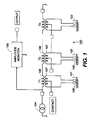
FIG. 1 is a schematic of a current driven test and measurement system in accord
with the present invention.
FIG. 2 is a schematic of a voltage driven test and measurement system in accord
with the present invention.
FIG. 3 is a detailed circuit schematic of a preferred embodiment of the present
invention.
DETAILED DESCRIPTION
Although the present invention is particularly well suited for monitoring the
integrity of electrical connections via split contacts and shall be described with respect
to this application, the apparatus disclosed here can be applied to other connection
types relying on conductive contacts.
Referring now to FIG. 1 there is shown a schematic of a current driven test and
measurement system 100 in accordance with the present invention. A series of
electrical contact pairs 101-103 are split into two individually spring loaded contact
pins 106. Each pair 101-103 of contact pins 106 are connected to the primary 107 of a
small center, tapped transformer, designated T1 to Tn respectively. The transformer
secondaries 108 are driven with an alternating current (AC) source 104. Additional
circuitry, for example, an amplitude monitor 105 then monitors the looking-in
impedance of the transformer secondaries in series. When both pins 106 of a contact
pair 101-103 contact a single land area, the corresponding transformer primary 107 is
short-circuited, thus, causing the reflected secondary impedance to become extremely
low. This contact condition is monitored continuously for all contacts, during all test
and measurement periods. This same scheme can be used for all signal, power and
ground leads, without restriction.
For the above-described secondary impedance measurement method, it will be
noted that the contact testing is absolutely continuous, while all measurements are
running. That is, the two halves of the primary are series opposing from the point of
view of all signal power and ground currents, which therefore link zero net flux with
the transformer core. Consequently the transformer is itself effectively invisible to both
the signal and power paths, while the contact is completely floating electrically.
Although at high frequencies (tens of MHz) the effects from primary leakage
inductance are evident, they can be circumvented by placing two equal small capacitors
across the two halves of each transformer primary, if necessary. To the extent that
there is any small residual coupling between different contacts, via the transformer
primary to secondary capacitances, this can be circumvented by the use of transformers
with electrostatic shields. In the event the lowering of the probes onto the contact area
creates a high resistance, a small oscillatory mechanical motion for the whole probe
head can be employed to in effect automatically "wipe" the contacts until all low
impedances are obtained. In fact, a simple wiping action could be an automatic part of
the lowering motion of the probe head, as would be understood by a person skilled in
the art.
There are various alternative embodiments in which the proposed reflected
impedance measurement can be made. The scheme shown in Fig. I drives all the
transformers T1 through Tn in series from a single alternating current source 104 and
then monitors the sum of the resulting voltage drops across the secondaries. Although
use of a current driven source is viable, there are some advantages with utilizing a
voltage to drive the transformers, as shown in Fig. 2. This system 200 of Fig. 2 adjusts
the radio frequency (RF) drive voltage amplitude until the current measured at a
current measurement device 203 is a certain fixed current as produced from a current
reference 202, and the quantity measured by the amplitude monitor 105 is the voltage
required to obtain that fixed current. One major advantage of the voltage driven system
200 is that in actual operation all of the transformer primaries and all of the
secondaries, T1 to Tn, are simultaneously, in effect, short-circuited. This has the result
of minimizing any potential crosstalk effects without requiring the use of
electrostatically shielded transformers, although such transformers can always be used,
if desired.
Referring now to FIG. 3, there is shown a detailed circuit schematic of one
preferred embodiment 300 of the present invention. The component values and part
numbers given in the parts list to follow, i.e., resistance, capacitance, inductance and
transistor part numbers, are illustrative only, and may be varied without straying from
the scope of the invention disclosed herein. The operational amplifiers utilized are well
known in the art. Essentially, an operational amplifier is a high gain device and many
suitable amplifiers are available commercially. Although only one transformer 303 is
shown rather then several transformers in series, one for each circuit, the system 300
operates as the system 200 in Fig. 2, with a monitoring circuit section 301, a radio
frequency drive voltage input section 302, and a current measuring circuit section 304
which includes a current reference circuit. The oscillating input circuit 302 includes an
L1C1 resonant circuit coupled to an operational amplifier 305 which is powered by two
twelve volt (12V) inputs of opposite polarity. The L1C1 tank circuit is preferably
tuned to a frequency of 160 kHz. The operational amplifier 305 is positively biased by
an output from the current measurement circuit 304 through a transistor, Q1, coupled
to a resistor R1 through which a negative twelve volts (-12V) is introduced. The
output of the amplifier 305 is coupled to a variable resistor RV1, a feedback loop to
the non-inverting (+) input of the amplifier 305 at terminal 3, and to the monitoring
section 301 at the base of transistor Q6.
The center tapped 1:1 transformer 303 is preferably one milli-henry (1mH), and
both contact legs 306 and 307 are shunted by capacitors C2 and C3, respectively, to
circumvent the effect of leakage inductance at the transformer primary from high
frequency oscillation voltages. In a test version of the circuit of FIG. 3, a transformer
303 was utilized having a physical configuration of 1.3 cm square by 7 mm high and a
primary to secondary capacitance of -3 Pico-farads (pf) has been utilized.
The current measuring section 304 is tuned to reduce the effect of any spurious
signals arising from the applied driving and switching voltages at the contacts. The
current measuring section 304 is coupled directly to the transformer 303 secondary leg,
labeled "2", through a capacitor C4 to the emitter of transistor Q3 and resistor R5.
The collector of Q3 is coupled to a resistor R4 which is in turn coupled to a twelve volt
(12V) supply applied through resistor R2 to the collector of transistor Q2. The base of
transistor Q2 is tapped to variable resistor RV1, and the emitter is coupled to a
negative twelve volt (-12V) supply through resistor R3 and coupled to the transformer
303 secondary leg, labeled "1". The collector of transistor Q3 is coupled through
capacitor C5 to an L2C6 tank circuit. Coupled across transistor Q3 and associated
resistors R4 and R5, transistor Q4 has its emitter coupled to a resistor R6, its collector
coupled to a resistor R7, and its base coupled to the L2C6 tank circuit and capacitor
C5. Coupled across resistor R6, are the collector and base of transistor Q5. The
emitter of transistor Q5 is coupled to a capacitor C7 and a resistor R8. Coupled from
resistors R8 and R7 is resistor R10 which is in turn coupled to capacitors C9 and C10
which are coupled to a negative twelve (12) volt supply. Resistors R10 and R8 are
coupled to an inverting (-) input to an operational amplifier 306 with positive and
negative biasing voltages of twelve (12) volts. The non-inverting (+) input of the
amplifier 306 is preferably tied to ground, as shown, and the output is partially fed-back
through a capacitor C8 to the inverting (-) input of the amplifier 306, i.e., a negative
feedback loop, and fed through a resistor R9 to the emitter of transistor Q1.
When the system 300 is operated, the demanded constant radio frequency (RF)
current flowing from pin-to-pin, i.e., 306 and 307, at each contact is defined by
resistors R8 and R10 and is set at a value of 2 milli-amperes, although it could readily
be higher if desired. This current provides the RF driving voltage, which itself is
monitored, and ensures that the contacts themselves remain electrically quiet.
The monitoring circuit section 301 produces current pulses, at the 160 kHz
carrier frequency, whenever the sum total of all the probe contact resistances rises
above the preset maximum value. As shown, the output of amplifier 305 is fed as a
base input to transistor Q6, which has its emitter coupled to resistors R11 and R13 and
its collector coupled to a resistor R15, which in turn is coupled to a negative twelve
(12) volt supply. Resistor R15 is coupled to the emitter of transistor Q7, and the
junction at resistor R11 and the collector of Q6 is coupled to a voltage divider, made
up of resistors R13 and R14, which are in turn coupled to the base of transistor Q7.
Resistor R11 is commonly coupled to resistor R12, the emitter of transistor Q8,
capacitors C11, C12, and C13, and a twelve (12) volt supply. Resistor R12 is tied to
the collector of transistor Q7 and the base of transistor Q8. The emitter of transistor
Q8, is fed back through a biasing diode D1 to the base of transistor Q8, and coupled to
the output point through a resistor R16. The preferred circuit embodiment 300 of Fig.
3 is preferably fabricated in surface mount technology to occupy an area of only 3 cm
by 4 cm, so as to be readily mounted close to any multi-pin probe head for actual high
reliability applications.
Description of the operation of the preferred circuit embodiment of FIG. 3
begins at the input where the oscillation amplitude out of the operational amplifier 305,
at pin 6, is 5 volts peak-to-peak (p-p) in the absence of a short circuit at the
transformer contacts 306 and 307. On shorting the contacts the total oscillation voltage
drops to a value such that the voltage across capacitor C7 is 2 volts, which requires an
RF voltage drive of only 100 milli-volts at the base of transistor Q2 base. It should be
noted that the emitter output impedance of transistor Q2 is 4 ohms, as is the emitter
input impedance of transistor Q3. Consequently, even with the variable resistor RV1
set for maximum amplitude, the 0.2 Volt threshold of the transistors Q6 and Q7 in the
current discriminator portion is not reached, and therefore, no output pulses are
observed. Of course the discriminator threshold can readily be raised by increasing the
resistance of R14, but for small numbers of contacts with appropriate transformers, this
should not be required.
In a final test of the effect of transients in the circuit of FIG. 3, the "connection"
point, at leg "1" of the transformer secondary was driven with 10 volt pulses of 0.1
micro seconds rise time at a 5 MHz repetition rate. Consistent with design
expectations, no system disturbance was observed since the winding-to-winding
capacitance of the transformer is only 3 pf while the capacitance of C6 is 10,000 pf.
This provides an attenuation of a factor of 3000, while at the same time the 160 kHz
signal of interest across the L2-C6 tank is 4 volts pp. An extremely high degree of
independence from signals at the contacts was observed. The same is true for contact-to-contact
crosstalk since both ends of the transformer strings are in effect at ground
while the winding to winding coupling capacitances are extremely small.
The following parts lists is illustrative of exemplary component values used in
conjunction with the embodiment shown in Fig. 2. Different component values and
other components may also be substituted as would be understood by a person skilled
in the art.
Component List
- R1
- 10K
- R2
- 100
- R3
- 2.7K
- R4
- 1K
- R5
- 2.7K
- R6
- 4.7K
- R7
- 100
- R8
- 22K
- R9
- 8.2K
- R10
- 120K
- R11
- 4.7K
- R12
- 2.2K
- R13
- 4.7K
- R14
- 220
- R15
- 10K
- R16
- 4.7K
- RV1
- 2.2K
- C1
- 10nf
- C2
- 1nf
- C3
- 1nf
- C4
- 0.1uf
- C5
- 10nf
- C6
- 10nf
- C7
- 1nf
- C8
- 01uf
- C9
- 47uf
- C10
- 0.1uf
- C11
- 0.1uf
- C12
- 47uf
- C13
- 0.1uf
- D1
- ZC2800
- L1
- 100uh
- L2
- 100uh
- Q1
- 2N3906
- Q2
- 2N3904
- Q3
- 2N3904
- Q4
- 2N3906
- Q5
- 2N3904
- Q6
- 2N3904
- Q7
- 2N3904
- Q8
- 2N3906
- 1C1
- LM3080
- 1C2
- LF351
From the above, it should be understood that the embodiments described, in regard
to the drawings, are merely exemplary and that a person skilled in the art may make
variations and modifications to the shown embodiments without departing from the spirit
and scope of the invention. All such variations and modifications are intended to be included
within the scope of the invention as defined in the appended claims.