EP0829048B1 - Programmierbare vorrichtung und verfahren zum befehlsauffang - Google Patents
Programmierbare vorrichtung und verfahren zum befehlsauffang Download PDFInfo
- Publication number
- EP0829048B1 EP0829048B1 EP96916908A EP96916908A EP0829048B1 EP 0829048 B1 EP0829048 B1 EP 0829048B1 EP 96916908 A EP96916908 A EP 96916908A EP 96916908 A EP96916908 A EP 96916908A EP 0829048 B1 EP0829048 B1 EP 0829048B1
- Authority
- EP
- European Patent Office
- Prior art keywords
- register
- trap
- instruction
- value
- bit
- Prior art date
- Legal status (The legal status is an assumption and is not a legal conclusion. Google has not performed a legal analysis and makes no representation as to the accuracy of the status listed.)
- Expired - Lifetime
Links
Images

Classifications
-
- G—PHYSICS
- G06—COMPUTING OR CALCULATING; COUNTING
- G06F—ELECTRIC DIGITAL DATA PROCESSING
- G06F11/00—Error detection; Error correction; Monitoring
- G06F11/36—Prevention of errors by analysis, debugging or testing of software
- G06F11/362—Debugging of software
- G06F11/3648—Debugging of software using additional hardware
Definitions
- This invention relates generally to data processors. More particularly, this invention relates to a system and method for providing programmable hardware instruction traps in a microprocessor.
- CPUs central processing units
- Many software application programs are not developed for use in a superscalar environment.
- a superscalar CPU executes instructions in such an application program some instructions may not perform in the manner they were designed.
- What is needed is a system and method for providing a programmable hardware device within a CPU that permits a plurality of instructions to be trapped before they are executed.
- the instructions that are to be trapped are programmable to provide flexibility during CPU debugging and to ensure that a variety of application programs can be properly executed by the CPU.
- the system must also provide a means for permitting a trapped instruction to be emulated and/or to be executed serially.
- EP-A-0 271 910 discloses a one-chip microprocessor having a break function.
- Break point registers are provided for holding user-set addresses or data values.
- Comparators are provided to compare the user-set addresses/data values in the break point registers with addresses to be accessed or data to be processed. If a break point register comparison delivers a match a break function may be executed.
- Means are provided for holding a history of break point register comparisons, and determination of whether a break condition is met may depend not only on a break point register comparison but also the history of other break point registers.
- the invention makes available a system and method that provides a programmable hardware device within a CPU.
- the programmable hardware device permits a plurality of instructions to be trapped before they are executed.
- the instructions that are to be trapped are programmable to provide flexibility during CPU debugging and to ensure that a variety of application programs can be properly executed by the CPU.
- the system must also provide a means for permitting a trapped instruction to be emulated and/or to be executed serially.
- FIG. 1 is an illustration of a computer environment in which a preferred embodiment of the present invention resides.
- a conventional memory unit 104 and conventional input/output (I/O) devices 106 communicate with a data processor 102.
- the processor is a HaL R1 processor developed by HaL Computer Systems, Campbell, California.
- the HaL R1 processor implements the SPARC V9 64 bit instruction set architecture developed by SPARC International, Inc., Menlo Park, California.
- the processor 102 includes a superscalar CPU 108, a memory management unit (MMU), and four cache memory units 110, 112.
- MMU memory management unit
- the cache memory units 110, 112 preferably include two 64 kilobyte (KB) conventional data caches and two 64 KB conventional instruction caches.
- the data caches 110 provide data to the superscalar CPU 108 and the MMU 114. Both sets of cache memory units 110, 112 are virtually indexed and tagged.
- Each cache chip 110, 112 contains 64 KB of data storage, organized as four sets.
- Each 64 KB cache chip 110, 112 can service two independent requests from the superscalar CPU 108.
- the interface between the superscalar CPU 108 and the caches 110, 112 is non-blocking in that the superscalar CPU 108 can access the cache 110, 112, at the same time a cache line is being refilled or flushed. Additional detail concerning the cache memory units 110, 112 is set forth in Chen, Chien, Y. Lu, A. Wond; The Microarchitecture of the HaL Cache, Compcon Proceedings 1995.
- the function of the MMU 114 includes controlling memory management and data coherence, interfacing to memory 104 and I/O devices 106, and error handling, for the processor 102.
- the MMU 114 includes three levels of address spaces: (1) a virtual address space for the processor 102, (2) a logical address space for I/O devices 106 and a diagnostic processor, and (3) a physical address space for memory 104. These hierarchical address spaces provide an efficient mechanism for managing the large address space.
- a more detailed description of the MMU 114 used in the preferred embodiment is described in David Chang, D. Lyon, C. Chen, L. Peng, M. Massoumi, M. Hakimi, S. Iyengar, E. Li, R. Remedios, Microarchitecture of HaL's Memory Management Unit, Compcon Proceedings 1995.
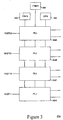
- FIG. 2 is a more detailed illustration of a superscalar CPU 108 of the preferred embodiment of the present invention.
- the processor 102 implements a four-stage pipeline for fixed-point instructions and a six-stage pipeline for "LOAD" instructions.
- the superscalar CPU 108 includes an instruction fetch unit 202, a programmable instruction trap unit 204, an instruction issue unit 206, an instruction execution unit 218, a precise state unit 220, a branch history table 208, a return prediction table 210, a prefetch buffer 212, a recoded instruction cache 214 and a branch unit 216.
- the fetch unit 202 requests and receives four instructions from either the off-chip 64 KB instruction cache 112, shown as data lines 201 in figure 2, a prefetch buffer 212, or a recoded instruction cache 214. Four instructions are then sent to a programmable instruction trap unit 204 to determine if any of the instructions should be trapped.
- the programmable instruction trap unit 204 is described in greater detail below with reference to figures 3-8.
- the branch history table 208 contains a plurality of counters that are used to predict the direction of execution branches.
- the return prediction table 210 is used to predict the return address of executed instructions.
- the branch unit 216 uses information from the issue unit 206, the branch history table 208, and the return prediction table 210, to determine if a control transfer instruction is within the current issue window, and further modifies the program counter if the control transfer instruction is taken.
- the issue unit 206 determines the available computer resources and issue constraints, e.g., should an instruction be synchronized. All instructions are issued by the issue unit 206 in the order they would have issued in a traditional serial processor and are sent to the instruction execution unit 218.
- the instruction execution unit 218 executes the instructions, although not necessarily in the order in which they were issued.
- the instruction execution unit 218 outputs the results of the instruction execution on data bus 222.
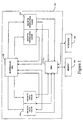
- FIG. 3 is a more detailed illustration of a programmable instruction trap unit 204 according to the preferred embodiment of the present invention.
- the programmable instruction trap unit 204 preferably receives four instructions from the fetch unit 202.
- the instructions are shown on figure 3 as INST00, INST01, INST10, IMST11.
- Each instruction is sent to an instruction trap logic unit (ITLU) 302.
- the instruction trap logic unit also receives signals from preferably four instruction trap register's (ITRV) 304, four instruction trap register masks (ITRM) 306, and four control registers (CR) 308.
- ITRV instruction trap register's
- ITRM instruction trap register masks
- CR control registers
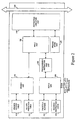
- FIG 4 is a more detailed illustration of a programmable instruction trap unit according to the preferred embodiment of the present invention.
- the instruction trap logic unit 302 preferably includes four Exclusive NOR logic devices 404A-D, where one Exclusive NOR is associated with each ITRV 304.
- Each Exclusive NOR device 404 compares each inverted bit of the instruction with a corresponding bit from the associated ITRV, e.g., ITRV0 410, and for each bit the NOR device 404 outputs a value indicating whether a match has occurred. It is envisioned that other techniques can be used to compare each bit of the instruction, INST00, with each bit in an ITRV 304. The method for performing this comparison is described in greater detail below with respect to figures 7-8.
- the instruction trap logic unit 302 preferably includes four devices 406A-D that compare each bit output by an associated Exclusive NOR device 404 with a bit value in an ITRM 306.
- Each ITRM 306 contains a plurality of bits containing a "care” or "don't care” value.
- Each of the four devices 406A-D compares a bit that is output by its associated Exclusive NOR device and a bit in its associated ITRM 306.
- Each device 406 outputs a one bit value representing whether all of the instruction bits match the associated ITRV-ITRM register pair.
- each device 406 is an AO32x2 device. This device has two sets of 32 bit inputs, one set coupled to each bit line of the associated Exclusive NOR 404 output, the other set coupled to the associated ITRM 306.
- the AO32x2 includes 32 logical AND gates whose outputs are input into a logical OR gate. The method for performing this comparison is described in greater detail below with respect to figures 7-8.
- the CR's 308 are associated with a single ITRV-ITRM pair.
- CR0 is associated with ITRV0 and ITRM0.
- Each CR contains data representing the action that is to be taken if the instruction matches its associated ITRV-ITRM register pair.
- each control register can contain any number of bits, in the preferred embodiment each CR 308 contains two bits. One bit represents a synchronization action, the other bit represent an instruction trap. That is, if the bits in a control register are "00" and if the instruction matches the associated ITRV-ITRM register pair 304, 306, then no special action is taken.
- the programmable instruction trap unit 204 will output a signal that causes the matched instruction to execute synchronously, i.e., all instructions that are issued before the matched instruction will have completed execution and the machine will be in a committed, i.e., known, state before the matched instruction executes.
- a synchronization instruction is issued, executed, completed and committed before any subsequent instructions are issued.
- the programmable instruction trap unit 204 will generate a non-synchronizing instruction issue trap, i,e., the instruction will take on the semantics of an instruction trap. If the bits in a control register are "11" and if the instruction matches the associated ITRV-ITRM register pair 304, 306, then the programmable instruction trap unit 204 will generate a synchronizing instruction issue trap, i.e., the instruction will be trapped and executed synchronously.
- the instruction trap logic unit 302 includes a device for generating the values stored in the CR 308 associated with an ITRV-ITRM register pair 304, 306 that matches the received instruction, e.g., INST00.
- a variety of techniques can be utilized to generate this value.
- two sets of four logical OR gates (one associated with each CR 308) receive an input from the CR 308.
- Each OR gate of the first set of OR gates receives two inputs: (1) the first bit of a CR 308, e.g., CR0, and (2) the one bit output from the AO32x2 associated with the CR 308.
- each OR gate of the second set of OR gates receives two inputs: (1) the second bit of a CR 308, e.g., CR0, and (2) the one bit output from the AO32x2 associated with the CR 308.
- the output of all of the OR gates for each set of OR gates is supplied to a logical NAND gate, 408A-B.
- the method for generating the outputs of the instruction trap logic unit 302 is described in greater detail below with respect to figures 7-8.
- the values in the ITRV's 304, the ITRM's 306, and the CR's 308 are programmable. These values can be programmed by a user to trap instructions and cause certain instructions to be executed synchronously, as described above.
- the programmability feature of the present invention provides an efficient technique for trapping and synchronizing instruction in order to correct functional errors in processor instructions and ensure the proper operation of application programs by executing certain instructions synchronously, i.e., those instructions stored in the ITRV 304, ITRM 306.
- a variety of techniques can be used to program the ITRV's 304, the ITRM's 306, and the CR's 308 (collectively called the programmable registers).
- the programmable registers can be coupled to a data bus and to control logic that permits the programmable registers to receive data from the data bus.
- the data is "scanned-in" during the computer boot-up operation.
- the programmable registers are programmed using a technique similar to shift registers.
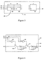
- FIG. 5 is a more detailed illustration of an ITRV 304 and ITRM 306 according to the preferred embodiment of the present invention.
- Each programmable register 410 contains a plurality of bit registers 502.
- each ITRV 304 and each ITRM 306 include 27 bit registers 502 while each CR 306 includes 2 bit registers 502.
- Figure 5 is a representative ITRV 304 or an ITRM 306.
- the CR's 308 operate in the same manner with the exception that each CR 308 preferably includes two bit registers 502 as opposed to 27 bit registers 502, as discussed above.
- Each programmable register 410 receives a scan clock (SC) signal, a scan-enable (SE) signal, and scan-input (SI) signal, and generates a scan-output (SO) signal and a Q output signal.
- SC scan clock
- SE scan-enable
- SI scan-input
- FIG. 6 is a more detailed illustration of a bit register 502 according to the preferred embodiment of the present invention.
- a signal containing a bit value is received on the SI line.
- the SC and SE signals are high, i.e., the signal represents a binary "1" value
- the logical AND gate 602 generates a high signal.
- This signal is coupled to the gate of transistor 604.
- transistor 604 conducts thereby enabling the signal on the SI line to pass through the transistor 604 and have its logic value be maintained by two inverters 606.
- the SC goes low while the SE signal remains high
- transistor 604 turns off and the logical AND gate 608 generates a high signal.
- the AND gate 608 is coupled to the gate of transistor 610.
- transistor 612 conducts and the inverted SI signal is again inverted by one of the inverters 610 and is output on the SO line.
- the signal is also output on the Q line that is coupled to either device 404A if the bit register is part of an ITRV 304 , an inverter and device 406A if the bit register is part of an ITRM 306, or an inverter and an OR gate if the bit register is part of a CR 308.
- the SO line is coupled to the next bit register SI line.
- the SO line of the last bit register of ITRV 304 is coupled to the first bit register of the first ITRM 306.
- the last bit register of ITRM 306 is coupled to the first bit register of the first CR 308.
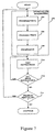
- Figure 7 is a flow diagram describing the method of trapping an instruction according to the preferred embodiment of the present invention.
- the ITRV's 304, the ITRM's 306, and the CR's 308 are programmed.
- these programmable registers can be programmed individually 704, 706, 708, using a data bus and control signals.
- the programmable registers are programmed during computer initialization using the scan-in, i.e., bit shifting, technique described above with reference to figures 5-6.
- the programmable registers are programmed 702 instructions are tested 710. The method for testing instructions is set forth below with respect to figure 8.
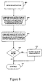
- Figure 8 is a flow diagram describing the method of testing an instruction according to the preferred embodiment of the present invention.
- Preferably four instructions are received 802 by the programmable instruction trap unit 204 from the fetch unit 202, as illustrated in figure 2.
- Each instruction is sent to a separate instruction trap logic unit 302.
- instruction INST00 is sent to instruction trap logic unit 302A.
- the instruction trap logic unit 302A inverts each bit in the instruction using inverter 402.
- the inverted instruction bits are received by four exclusive NOR device 404A-D, described above with reference to figure 4.
- Each exclusive NOR device 404 compares 804 each inverted instruction bit with a corresponding bit in one of the ITRV's 304 that was previously programmed.
- the exclusive NOR device 404A compares instruction bit 0 with bit register 0 of ITRV0 as illustrated in figures 4-6. If the inverted instruction bit matches the associated bit in one of the ITRV's 304 then the exclusive NOR generates a signal representing a logical "1". Otherwise, the exclusive NOR generates a signal representing a logical "0". Since the exclusive NOR device is comparing the associated ITRV bit register 502 and an inverted bit of the instruction, if the exclusive NOR generates a signal representing a logical "0" then the ITRV bit matches the instruction bit. Each inverted bit of the instruction, INST00, is compared to each associated bit of each ITRV 304. Preferably, the result of these comparisons is four 27-bit signals representing the result of the exclusive NOR comparison of devices 404A-D.
- each bit in each set of 27-bit signals is compared 806 with a bit register 502 in an associated ITRM 306 using an AO32x2 device 406A-D.
- Each AO32x2 device 406A-D consists of at least 27 logical AND gates whose outputs are input into a logical OR gate.
- the least significant bit, or the zero bit, that is output from device 404A is input into an AND gate along with the inverted zero bit register of ITRM0.
- the ITRM's 306 are a mask.
- it is desirable to compare each instruction with a set of related instruction patterns For example, it may be desirable to match all instructions having a certain combination of bits 5-9.
- the remaining bits e.g., bits 0-4 and 10-26
- the "don't care” value is a logical "1".
- the ITRM values are inverted before they are received by the AO32x2. Accordingly, if a bit from device 404A is either zero, because the instruction bit matched the associated ITRV bit register, the output of the associated AND gate in the AO32x2 406A will be zero. Similarly, if a bit from device 404A is a logical one, then the output of the AND will be zero only if the associated bit register in ITRM0 is masked, i.e., it's inverted value is equal to zero.
- the AND gate outputs are coupled to an OR gate. If any AND gate output is a logical one then the output of the OR gate is a logical one.
- the output of the OR gate is the output of the AO32x2 406. Therefore, the AO32x2 406 generates an instruction match value (IMV) signal that represents a logical zero only if all of the bits from the instruction INST00 either match the associated ITRV bits or are masked, i.e., if the instruction INST00 matches the ITRV-ITRM 304, 306 register pair.
- IMV instruction match value
- the programmable instruction trap unit 204 determines 810 if any matches have occurred and if so it generates 812 the value in the associated CR 308. The process for achieving this is now described.
- the output from each AO32x2 device 406 is received by two logical OR gates, e.g., OR gates 418, 420, as illustrated in figure 4.
- the second input to the first OR gate 418 is the value of the first bit register of the associated CR 308.
- the second input to the second OR gate 420 is the value of the second bit register of the associated CR 308.
- AO32x2 406A generates a signal representing a logical zero at its output and the remaining AO32x2 406B-D generate a signal representing a logical one at its output.
- the three OR gates associated with AO32x2's 406B-D receive a binary one as one of its inputs. Accordingly, these three OR gates will output a signal representing a binary one.
- NAND gate 408A will generate a logical zero output only if the output of OR gate 418 generates a logical one.
- OR gate 418 is a logical one only if the first bit register of CR0 contains a logical zero.
- Each set of four OR gates and one NAND gate 408 result in either (1) the value of the CR 308 associated with a matching register pair to be output by the NAND gates 408A-B, or (2) if the instruction INST00 does not match any register pair, the NAND gates 408A-B output a "00" value representing that no special action is to be taken, as described above.
- All four received instructions i.e., INST00, INST01, INST10, and INST11 are similarly compared to each of the four ITRV registers and the ITRM registers.
- both the register pair ITRV1-ITRM1 and the register pair ITRV2-ITRM2 can match a particular instruction, e.g., INST00.
- a bit value of "1" in a CR bit register for one CR e.g., CR2
- the method continues 814. If more instructions are received 712 the process repeats. After all instructions have been tested new values for the ITRV's 304, ITRM's 306, and CR's 308 can be programmed 714 in using a data bus or preferably by rebooting the computer and scanning in new programmable register values, as described above, and then the process 702-714 repeats.
Landscapes
- Engineering & Computer Science (AREA)
- Computer Hardware Design (AREA)
- Theoretical Computer Science (AREA)
- Quality & Reliability (AREA)
- Physics & Mathematics (AREA)
- General Engineering & Computer Science (AREA)
- General Physics & Mathematics (AREA)
- Debugging And Monitoring (AREA)
- Advance Control (AREA)
- Executing Machine-Instructions (AREA)
Claims (5)
- Computerverarbeitungssystem, aufweisend:eine Befehlsabrufeinheit (202), die angeordnet ist, um mehrere Computerbefehle zu empfangen, zum Wiedergewinnen der mehreren Computerbefehle;eine programmierbare Befehlsfangstelleneinheit (204), die mit der Befehlsabrufeinheit (202) gekoppelt ist, mit:mehreren Registerpaaren (304 & 306, ITRV0 & ITRM0 - ITRV3 & ITRM3), jedes Registerpaar aufweisend
ein Werteregister (304, ITRV0 - ITRV3) zum Speichern eines Fang-Wertes, der einen oder mehrere Fang-Befehle repräsentiert, die ein Benutzer abfangen möchte, welcher Fang-Wert vom Nutzer programmierbar ist, und
ein Maskenregister (306, ITRM0 - ITRM3) zum Speichern von Maskeninformation, die dem Werteregister des Paars zugeordnet ist;mehreren Komparatoren (404A - 404D, XNOR2), die jeweils angeordnet sind, um einen Computerbefehl (INST0, INST1, INST2, INST3) und einen Fang-Wert von einem der Registerpaare zu empfangen und den Computerbefehl und den betreffenden Fang-Wert zu vergleichen, um ein Vergleichsergebnis zu liefern;mehreren Maskiervorrichtungen (406A - 406D, AO32X2), die jeweils programmierbar sind, um die Maskeninformation von einem der Registerpaare auf das Vergleichsergebnis anzuwenden, das von demjenigen Komparator geliefert wurde, der angeordnet ist, um den Fang-Wert vom gleichen Registerpaar zu empfangen, um ein maskiertes Vergleichsergebnis zu liefern, auf dessen Basis bestimmt wird, ob der Computerbefehl und der Fang-Wert als zusammenpassend betrachtet werden,mehreren programmierbaren Steuerregistern (308, CR0 - CR3), die jeweils einem der Registerpaare zugeordnet sind, um Daten zu enthalten, die eine Funktion darstellen, die ausgeführt werden soll, falls bestimmt wird, dass ein Computerbefehl und der Fang-Wert des zugeordneten Registerpaares als zusammenpassend betrachtet werden, undeiner mit den Steuerregistern (308, CR0 - CR3) gekoppelten Steuereinheit (418, 420, 408A, 408B), die betreibbar ist, um Befehlsfangstellen-Steuersignale zu erzeugen, die die Funktion repräsentieren, die durch die in einem Steuerregister enthaltenen Daten repräsentiert wird, falls bestimmt wird, dass ein Computerbefehl und der Fang-Wert des dem Steuerregister zugeordneten Registerpaares als zusammenpassend betrachtet werden. - Computerverarbeitungssystem nach Anspruch 1, worin jeder der Komparatoren (404A - 404D, XNOR2) betreibbar ist, um jedes Bit eines Computerbefehls (INST0, INST1, INST2, INST3) mit einem entsprechenden Bit des betreffenden Fang-Wertes zu vergleichen, und das Vergleichsergebnis Bits aufweist, die jeweils angeben, ob verglichene entsprechende Bits zusammenpassen oder nicht zusammenpassen, und
die auf ein Vergleichsergebnis angewendete Maskierinformation Bits aufweist, die entweder "Beachten" oder "Nicht Beachten" in Bezug auf jedes Bit des Vergleichsergebnisses angeben, welche Maskiervorrichtungen (406A - 406D, AO32X2) betreibbar sind, um die Maskierinformation derart anzuwenden, dass jedes Bit "Nicht Beachten" des Vergleichsergebnisses, das ein Nicht-Zusammenpassen angibt, maskiert wird, so dass ein Zusammenpassen im maskierten Vergleichsergebnis angegeben wird. - Computerverarbeitungssystem nach Anspruch 1, worin vier Befehle (INST0, INST1, INST2, INST3) gleichzeitig einem Abfangen in der Befehlsfangstelleneinheit unterzogen werden.
- Verfahren zum Identifizieren abzufangender Befehle, mit den folgenden Schritten:Programmieren in mehrere Registerpaare, wobei jedes Registerpaar ein Werteregister (304, ITRV0 - ITRV3) und einem Maskenregister (306, ITRM0 - ITRM3) aufweist, wie folgt(a) in die Werteregister (304, ITRV0 - ITRV3), Programmieren jeweiliger Fang-Werte, die einen oder mehrere Fang-Befehle repräsentieren, die ein Nutzer abfangen möchte,(b) in die Maskenregister (306, ITRM0 - ITRM3), Programmieren jeweiliger Elemente einer Maskeninformation, die dem Fang-Wert zugeordnet ist, der in das Werteregister des gleichen Registerpaares programmiert wurde;Programmieren in mehrere Steuerregister (308, CR0 - CR3), die jeweils mit einem der Registerpaare verbunden sind, von Daten, die eine Funktion repräsentieren, die ausgeführt werden soll, falls bestimmt wird, dass ein Computerbefehl und der Fang-Wert des zugeordneten Registerpaares als zusammenpassend betrachtet werden,Empfangen von Computerbefehlen (INST0, INST1, INST2, INST3) und Durchführen von Vergleichen (404A - 404D, XNOR2) der Computerbefehle (INST0, INST1, INST2, INST3) und der in die Registerpaare programmierten Fang-Werte, um Vergleichsergebnisse zu liefern;auf jedes Vergleichsergebnis, Anwenden der Maskeninformation vom gleichen Registerpaar (406A - 406D, AO32X2), wie durch den Fang-Wert vorgesehen, der im Vergleich verwendet wurde, um ein maskiertes Vergleichsergebnis zu liefern, auf dessen Basis bestimmt wird, ob der Computerbefehl und der Fang-Wert als zusammenpassend betrachtet werden, undErzeugen von Befehlsfangstellen-Steuersignale (418, 420, 408A, 408B), die die Daten darstellen, die in das einem Registerpaar zugeordnete Steuerregister (308, CR0 - CR3) programmiert wurden, falls bestimmt wird, dass ein Computerbefehl und der in das betreffende Registerpaar programmierte Fang-Wert als zusammenpassend betrachtet werden.
- Verfahren nach Anspruch 4, worin in jedem Vergleich (404A - 404D, XNOR2) jedes Bit eines Computerbefehls mit einem entsprechenden Bit des betreffenden Fang-Wertes verglichen wird und das Vergleichsergebnis Bits aufweist, die jeweils angeben, ob verglichene entsprechende Bits zusammenpassen oder nicht zusammenpassen, und die auf ein Vergleichsergebnis angewendete Maskierinformation Bits aufweist, die entweder "Beachten" oder "Nicht Beachten" in Bezug auf jedes Bit des Vergleichsergebnisses angeben, welche Maskierinformation angewendet wird (406A - 406D, AO32X2), so dass jedes Bit "Nicht Beachten" des Vergleichsergebnisses, das ein Nicht-Zusammenpassen angibt, maskiert wird, so dass ein Zusammenpassen im maskierten Vergleichsergebnis angegeben wird.
Applications Claiming Priority (3)
| Application Number | Priority Date | Filing Date | Title |
|---|---|---|---|
| US45674695A | 1995-06-01 | 1995-06-01 | |
| US456746 | 1995-06-01 | ||
| PCT/US1996/008256 WO1996038789A2 (en) | 1995-06-01 | 1996-05-31 | Programmable instruction trap system and method |
Publications (2)
| Publication Number | Publication Date |
|---|---|
| EP0829048A2 EP0829048A2 (de) | 1998-03-18 |
| EP0829048B1 true EP0829048B1 (de) | 2003-02-19 |
Family
ID=23813986
Family Applications (1)
| Application Number | Title | Priority Date | Filing Date |
|---|---|---|---|
| EP96916908A Expired - Lifetime EP0829048B1 (de) | 1995-06-01 | 1996-05-31 | Programmierbare vorrichtung und verfahren zum befehlsauffang |
Country Status (5)
| Country | Link |
|---|---|
| US (1) | US5896526A (de) |
| EP (1) | EP0829048B1 (de) |
| JP (1) | JP3604697B2 (de) |
| DE (1) | DE69626282T2 (de) |
| WO (1) | WO1996038789A2 (de) |
Families Citing this family (7)
| Publication number | Priority date | Publication date | Assignee | Title |
|---|---|---|---|---|
| FR2765701B1 (fr) * | 1997-07-03 | 1999-08-20 | Sgs Thomson Microelectronics | Circuit de detection d'anomalie d'acces a la pile dans un microcontroleur |
| GB9805485D0 (en) * | 1998-03-13 | 1998-05-13 | Sgs Thomson Microelectronics | Microcomputer |
| GB9805486D0 (en) | 1998-03-13 | 1998-05-13 | Sgs Thomson Microelectronics | Adapter |
| DE10057780A1 (de) * | 2000-11-22 | 2002-06-06 | Siemens Ag | Verfahren zum Betrieb einer programmierbaren Steuereinrichtung |
| WO2005008386A2 (en) * | 2003-07-07 | 2005-01-27 | Mformation Technologies, Inc. | System and method for over the air (ota) wireless device and network management |
| EP1908196B1 (de) * | 2005-07-28 | 2012-11-07 | Mformation Technologies, Inc. | System und verfahren zur verwaltung der dienstqualität drahtloser geräte |
| EP1907901B1 (de) * | 2005-07-28 | 2017-01-18 | Alcatel Lucent | System und verfahren zur fernsteuerung von gerätefunktionen |
Family Cites Families (12)
| Publication number | Priority date | Publication date | Assignee | Title |
|---|---|---|---|---|
| US3937938A (en) * | 1974-06-19 | 1976-02-10 | Action Communication Systems, Inc. | Method and apparatus for assisting in debugging of a digital computer program |
| US4635193A (en) * | 1984-06-27 | 1987-01-06 | Motorola, Inc. | Data processor having selective breakpoint capability with minimal overhead |
| JPS63155336A (ja) * | 1986-12-19 | 1988-06-28 | Hitachi Ltd | デ−タ処理装置 |
| US4905242A (en) * | 1987-06-09 | 1990-02-27 | The United States Of America As Represented By The Secretary Of The Air Force | Pipelined error detection and correction apparatus with programmable address trap |
| JPH0769783B2 (ja) * | 1987-11-16 | 1995-07-31 | 日本電気株式会社 | 例外処理方式 |
| US4996688A (en) * | 1988-09-19 | 1991-02-26 | Unisys Corporation | Fault capture/fault injection system |
| US5327567A (en) * | 1989-11-16 | 1994-07-05 | Texas Instruments Incorporated | Method and system for returning emulated results from a trap handler |
| JPH04257932A (ja) * | 1991-02-13 | 1992-09-14 | Oki Electric Ind Co Ltd | ディジタルシグナルプロセッサのエミュレート用チップ |
| US5491793A (en) * | 1992-07-31 | 1996-02-13 | Fujitsu Limited | Debug support in a processor chip |
| JPH06161822A (ja) * | 1992-11-20 | 1994-06-10 | Mitsubishi Electric Corp | マイクロプロセッサ |
| EP0636976B1 (de) * | 1993-07-28 | 1998-12-30 | Koninklijke Philips Electronics N.V. | Mikrokontroller mit hardwaremässiger Fehlerbeseitigungsunterstützung nach dem Boundary-Scanverfahren |
| US5488688A (en) * | 1994-03-30 | 1996-01-30 | Motorola, Inc. | Data processor with real-time diagnostic capability |
-
1996
- 1996-05-31 EP EP96916908A patent/EP0829048B1/de not_active Expired - Lifetime
- 1996-05-31 WO PCT/US1996/008256 patent/WO1996038789A2/en not_active Ceased
- 1996-05-31 JP JP53674596A patent/JP3604697B2/ja not_active Expired - Lifetime
- 1996-05-31 DE DE69626282T patent/DE69626282T2/de not_active Expired - Lifetime
-
1998
- 1998-02-18 US US09/025,511 patent/US5896526A/en not_active Expired - Lifetime
Also Published As
| Publication number | Publication date |
|---|---|
| EP0829048A2 (de) | 1998-03-18 |
| DE69626282D1 (de) | 2003-03-27 |
| DE69626282T2 (de) | 2004-04-08 |
| WO1996038789A2 (en) | 1996-12-05 |
| JP2000504444A (ja) | 2000-04-11 |
| WO1996038789A3 (en) | 1997-01-09 |
| JP3604697B2 (ja) | 2004-12-22 |
| US5896526A (en) | 1999-04-20 |
Similar Documents
| Publication | Publication Date | Title |
|---|---|---|
| EP0331372B1 (de) | Verfahren und Gerät zur Steuerung von prozessoren mittels Vorhersagen von Ausnahmen bei der gleitkomma-Arithmetik | |
| US5226130A (en) | Method and apparatus for store-into-instruction-stream detection and maintaining branch prediction cache consistency | |
| US5867644A (en) | System and method for on-chip debug support and performance monitoring in a microprocessor | |
| US5956477A (en) | Method for processing information in a microprocessor to facilitate debug and performance monitoring | |
| US5421022A (en) | Apparatus and method for speculatively executing instructions in a computer system | |
| US5375212A (en) | System for re-execution of instruction after exception handling in first processing path while concurrently executing instructions in second processing path | |
| US6052774A (en) | Apparatus and method for identifying exception routines indicated by instruction address issued with an instruction fetch command | |
| US5450560A (en) | Pointer for use with a buffer and method of operation | |
| US5880671A (en) | Flexible circuitry and method for detecting signal patterns on a bus | |
| AU613217B2 (en) | Data processing apparatus | |
| US5838897A (en) | Debugging a processor using data output during idle bus cycles | |
| EP0378830A2 (de) | Verfahren und Vorrichtung zur Verarbeitung von mehreren Zustandscodes wie für einen Parallel-Pipeline-Rechner | |
| US5956476A (en) | Circuitry and method for detecting signal patterns on a bus using dynamically changing expected patterns | |
| JP4012377B2 (ja) | 通常モードでの命令実行中にハードウェア・テストを実行するプロセッサおよび方法 | |
| JPS5911943B2 (ja) | デ−タ処理装置の為のトラツプ機構 | |
| WO1999054809A9 (en) | Real time debugger interface for embedded systems | |
| KR100335744B1 (ko) | 로드/로드 검출 및 재정렬 방법 | |
| US4520440A (en) | Test verification of processor architecture having a partial instruction set | |
| WO1993009492A2 (en) | Out of order job processing method and apparatus | |
| US5887003A (en) | Apparatus and method for comparing a group of binary fields with an expected pattern to generate match results | |
| US5649137A (en) | Method and apparatus for store-into-instruction-stream detection and maintaining branch prediction cache consistency | |
| US5592674A (en) | Automatic verification of external interrupts | |
| EP0829048B1 (de) | Programmierbare vorrichtung und verfahren zum befehlsauffang | |
| US5881224A (en) | Apparatus and method for tracking events in a microprocessor that can retire more than one instruction during a clock cycle | |
| KR100351527B1 (ko) | 코드브레이크포인트디코더 |
Legal Events
| Date | Code | Title | Description |
|---|---|---|---|
| PUAI | Public reference made under article 153(3) epc to a published international application that has entered the european phase |
Free format text: ORIGINAL CODE: 0009012 |
|
| 17P | Request for examination filed |
Effective date: 19971222 |
|
| AK | Designated contracting states |
Kind code of ref document: A2 Designated state(s): DE FR GB |
|
| 17Q | First examination report despatched |
Effective date: 20010201 |
|
| RAP1 | Party data changed (applicant data changed or rights of an application transferred) |
Owner name: FUJITSU LIMITED |
|
| GRAG | Despatch of communication of intention to grant |
Free format text: ORIGINAL CODE: EPIDOS AGRA |
|
| GRAG | Despatch of communication of intention to grant |
Free format text: ORIGINAL CODE: EPIDOS AGRA |
|
| GRAH | Despatch of communication of intention to grant a patent |
Free format text: ORIGINAL CODE: EPIDOS IGRA |
|
| GRAH | Despatch of communication of intention to grant a patent |
Free format text: ORIGINAL CODE: EPIDOS IGRA |
|
| GRAA | (expected) grant |
Free format text: ORIGINAL CODE: 0009210 |
|
| AK | Designated contracting states |
Designated state(s): DE FR GB |
|
| REG | Reference to a national code |
Ref country code: GB Ref legal event code: FG4D |
|
| REF | Corresponds to: |
Ref document number: 69626282 Country of ref document: DE Date of ref document: 20030327 Kind code of ref document: P |
|
| ET | Fr: translation filed | ||
| PLBE | No opposition filed within time limit |
Free format text: ORIGINAL CODE: 0009261 |
|
| STAA | Information on the status of an ep patent application or granted ep patent |
Free format text: STATUS: NO OPPOSITION FILED WITHIN TIME LIMIT |
|
| 26N | No opposition filed |
Effective date: 20031120 |
|
| PGFP | Annual fee paid to national office [announced via postgrant information from national office to epo] |
Ref country code: FR Payment date: 20110523 Year of fee payment: 16 |
|
| PGFP | Annual fee paid to national office [announced via postgrant information from national office to epo] |
Ref country code: GB Payment date: 20110525 Year of fee payment: 16 |
|
| PGFP | Annual fee paid to national office [announced via postgrant information from national office to epo] |
Ref country code: DE Payment date: 20110525 Year of fee payment: 16 |
|
| GBPC | Gb: european patent ceased through non-payment of renewal fee |
Effective date: 20120531 |
|
| REG | Reference to a national code |
Ref country code: FR Ref legal event code: ST Effective date: 20130131 |
|
| REG | Reference to a national code |
Ref country code: DE Ref legal event code: R119 Ref document number: 69626282 Country of ref document: DE Effective date: 20121201 |
|
| PG25 | Lapsed in a contracting state [announced via postgrant information from national office to epo] |
Ref country code: GB Free format text: LAPSE BECAUSE OF NON-PAYMENT OF DUE FEES Effective date: 20120531 Ref country code: FR Free format text: LAPSE BECAUSE OF NON-PAYMENT OF DUE FEES Effective date: 20120531 |
|
| PG25 | Lapsed in a contracting state [announced via postgrant information from national office to epo] |
Ref country code: DE Free format text: LAPSE BECAUSE OF NON-PAYMENT OF DUE FEES Effective date: 20121201 |