EP0825518A1 - Circuit de remise à zéro pour passerelle de bus PCI - Google Patents
Circuit de remise à zéro pour passerelle de bus PCI Download PDFInfo
- Publication number
- EP0825518A1 EP0825518A1 EP97306155A EP97306155A EP0825518A1 EP 0825518 A1 EP0825518 A1 EP 0825518A1 EP 97306155 A EP97306155 A EP 97306155A EP 97306155 A EP97306155 A EP 97306155A EP 0825518 A1 EP0825518 A1 EP 0825518A1
- Authority
- EP
- European Patent Office
- Prior art keywords
- input
- gate
- output
- pci
- bus
- Prior art date
- Legal status (The legal status is an assumption and is not a legal conclusion. Google has not performed a legal analysis and makes no representation as to the accuracy of the status listed.)
- Withdrawn
Links
Images
Classifications
-
- G—PHYSICS
- G06—COMPUTING; CALCULATING OR COUNTING
- G06F—ELECTRIC DIGITAL DATA PROCESSING
- G06F13/00—Interconnection of, or transfer of information or other signals between, memories, input/output devices or central processing units
- G06F13/38—Information transfer, e.g. on bus
- G06F13/40—Bus structure
- G06F13/4004—Coupling between buses
- G06F13/4027—Coupling between buses using bus bridges
-
- G—PHYSICS
- G06—COMPUTING; CALCULATING OR COUNTING
- G06F—ELECTRIC DIGITAL DATA PROCESSING
- G06F1/00—Details not covered by groups G06F3/00 - G06F13/00 and G06F21/00
- G06F1/24—Resetting means
Definitions
- the present invention relates to reset circuits for computer systems utilizing a peripheral component interconnect (PCI) environment. More specifically, the present invention relates to a reset circuit for resetting a PCI bus within a computer system.
- PCI peripheral component interconnect
- PCI peripheral component interconnect
- the PCI bus is a system bus that can be populated with adapters requiring fast access to memory or each other.
- the PCI bus is a bus-mastered architecture.
- a bus-mastered approach allows for a single bus master which controls the bus and generally a single target device for any given transaction.
- One advantage of the PCI bus over other technologies is that the length of a burst transfer is negotiated by master and target rather than limited to a finite number of words.
- the PCI bus uses burst mode to read and write data to and from adapters. Data is transferred every clock cycle, as opposed to very other clock cycle as is the case in some other bus designs.
- the PCI bus can provide up to 132 Mbits/sec performance during burst mode operation for 32-bit systems, and up to 264 Mbits/sec performance during burst mode operation for 64-bit systems.
- the PCI bus is configured so that it is not directly connected to the processor and memory. The reason for this is that bus designs that are wired directly to the processor are limited in the number of devices they can support, usually three. The PCI bus however can support up to ten or more devices.
- a PCI host bridge (or bus controller chip or module) is connected between the central processing unit (CPU) and the PCI busses.
- the bridge acts as a buffer between the CPU and the PCI busses and also maintains the PCI bus in synch with the CPU.
- a problem encountered with certain PCI chip sets occurs when a user attempts to assert a warm boot on the computer system.
- a warm boot is generated, for example by entering Ctrl-Alt-Delete
- certain PCI chip sets such as the Intel 440FX PCIset
- the present invention overcomes the above identified problems as well as other shortcomings and deficiencies of existing technologies by providing a PCI reset circuit that resets the PCI bus in response to the assertion of a warm boot command, either by hardware, software, or the user of the computer system.
- the present invention further provides a computer system having a host data bus; a peripheral component interconnect(PCI) data bus; a PCI host bridge connected between the host data bus and the PCI data bus, which is for interfacing data between the host data bus and the PCI data bus; and a reset circuit connected between the PCI host bridge and the PCI data bus for resetting the PCI data bus in the event of a warm boot in the computer system.
- the reset circuit includes a delay device and programmable array logic.
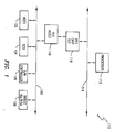
- the computer system 110 includes a processor 112, a host data bus 114, a peripheral component interface (PCI) chip set 116, a PCI reset 118, a PCI data bus 120 and multiple input/outputs such as video I/O 122, SCSI 124, LAN controller 126 and ISA/EISA bridge 128.
- PCI peripheral component interface
- processor 112 and PCI chip set 116 are connected to host data bus 114, while PCI reset 118 is connected between PCI chip set 116 and PCI data bus 120.
- PCI data bus 120 is in turn connected to various input/output (I/O) ports such as the ports of video I/O 122, SCSI 124, LAN controller 126 and ISA/EISA bridge 128.
- I/O input/output
- Both PCI data bus 120 and host data bus 114 generally consist of a control line, an address line and a data line.
- the Intel 440FX PCIset generally includes a PCI & memory controller (PMC) chip (the 82441FX PMC), a data bus accelerator (DBX) chip (the 8244FX DBX), and a PCI ISA IDE Accelerator chip (the PIIX3).
- PMC PCI & memory controller
- DBX data bus accelerator
- PIIX3 PCI ISA IDE Accelerator chip
- computer system 110 is depicted as utilizing a single processor, it is also contemplated that multiple processors could be used.
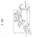
- PCI reset 118 is connected to PMC 210, which as described above, is one of the chips utilized by PCI chip set 116.
- PMC 210 includes signal outputs 212 and 214, where output 212 generates the cold boot PMC/PCI reset signal and output 214 generates a flush signal.
- PCI reset 118 includes a logical AND gate 216, a logical OR gate 224, an inverter 232, and a delay device 238.
- AND gate 216 includes inputs 218 and 220 and an output 222.
- Output 222 is connected to PCI data bus 120 and outputs the PCI reset signal.
- the input 218 of AND gate 216 is connected to output 212 of PMC 210.
- OR gate 224 includes inputs 226 and 228 and an output 230. Output 230 of OR gate 224 is connected to input 220 of AND gate 216. Input 226 of OR gate 224 is connected to output 214 of PMC 210.
- Inverter 232 includes an input 234 and an output 236. Input 234 of inverter 232 is connected to output 214 of PMC 210. As further illustrated, delay device 238 includes a resistor 240, and a capacitor 242, with resistor 240 connected between output 236 of inverter 232 and input 228 of OR gate 224 and capacitor 242 connected between a potential (illustrated as ground) and input 228 of OR gate 224. The values of resistor 240 and capacitor 242 will vary depending upon the desired delay. Although good results have been achieved with the above described delay device, it is contemplated that other delay devices could be utilized in the present invention by one skilled in the art.
- PCI reset 118 In the initial or normal operating state, the cold boot PCI/PMC signal at output 212 is high, and is only asserted low in response to a cold boot event; the PCI reset signal at output 222 is normally high and the flush signal at output 214 is also normally high. This correlates to a high signal at input 218 of AND gate 216 and at input 226 of OR gate 224, a low signal at input 228 of OR gate 224; and a high signal at output 230 and input 220.
- PMC 210 is instructed to assert the flush signal at output 214 (change it from high to low). This causes the input at input 226 of OR gate 224 to go low, and because of delay device 238 the input at input 228 or OR gate 224 is delayed from going from low to high. This causes the signal at output 230 of OR gate 224 to become low.
- AND gate 216 now has a high signal at input 218 and a low signal 220, thereby causing the PCI reset signal at output 220 to be asserted (change from high to low) and resetting PCI bus 120.
- the signal at input 228 switches from low to high causing the signal at output 230 to switch back high, which in turn releases the PCI reset signal (goes from low to high) thereby allowing the system to restart.
- delay device 238 When using the Intel 440FX PCIset, good results have been achieved in the present invention by configuring delay device 238 to provide an approximate 8 millisecond delay. This is achieved by using a 100 Kohm resistor for resistor 240 and a 0.22 microfarad capacitor for capacitor 242.
Applications Claiming Priority (2)
| Application Number | Priority Date | Filing Date | Title |
|---|---|---|---|
| US08/699,918 US5867676A (en) | 1996-08-20 | 1996-08-20 | Reset circuit for a peripheral component interconnect bus |
| US699918 | 1996-08-20 |
Publications (1)
| Publication Number | Publication Date |
|---|---|
| EP0825518A1 true EP0825518A1 (fr) | 1998-02-25 |
Family
ID=24811478
Family Applications (1)
| Application Number | Title | Priority Date | Filing Date |
|---|---|---|---|
| EP97306155A Withdrawn EP0825518A1 (fr) | 1996-08-20 | 1997-08-13 | Circuit de remise à zéro pour passerelle de bus PCI |
Country Status (3)
| Country | Link |
|---|---|
| US (1) | US5867676A (fr) |
| EP (1) | EP0825518A1 (fr) |
| JP (1) | JPH1097491A (fr) |
Cited By (1)
| Publication number | Priority date | Publication date | Assignee | Title |
|---|---|---|---|---|
| CN100375941C (zh) * | 2004-12-10 | 2008-03-19 | 威盛电子股份有限公司 | 计算机系统及系统重置方法 |
Families Citing this family (6)
| Publication number | Priority date | Publication date | Assignee | Title |
|---|---|---|---|---|
| US5996038A (en) * | 1998-01-26 | 1999-11-30 | Intel Corporation | Individually resettable bus expander bridge mechanism |
| US5991900A (en) * | 1998-06-15 | 1999-11-23 | Sun Microsystems, Inc. | Bus controller |
| US6763458B1 (en) | 1999-09-27 | 2004-07-13 | Captaris, Inc. | System and method for installing and servicing an operating system in a computer or information appliance |
| CN100403288C (zh) * | 2006-09-01 | 2008-07-16 | 威盛电子股份有限公司 | 具有重置功能的高速pci接口系统及其重置方法 |
| CN101206516B (zh) * | 2006-12-19 | 2012-05-30 | 鸿富锦精密工业(深圳)有限公司 | 计算机系统重置装置 |
| KR20150025782A (ko) | 2013-08-30 | 2015-03-11 | 에스케이하이닉스 주식회사 | 메모리 장치 및 이를 포함하는 컴퓨터 시스템 |
Citations (1)
| Publication number | Priority date | Publication date | Assignee | Title |
|---|---|---|---|---|
| EP0158512A2 (fr) * | 1984-04-05 | 1985-10-16 | Mitsubishi Denki Kabushiki Kaisha | Circuit de remise à l'état initial |
Family Cites Families (6)
| Publication number | Priority date | Publication date | Assignee | Title |
|---|---|---|---|---|
| US5446403A (en) * | 1994-02-04 | 1995-08-29 | Zenith Data Systems Corporation | Power on reset signal circuit with clock inhibit and delayed reset |
| WO1995031777A1 (fr) * | 1994-05-18 | 1995-11-23 | Intel Corporation | Procede et appareil permettant de configurer plusieurs agents dans un systeme informatique |
| US5657455A (en) * | 1994-09-07 | 1997-08-12 | Adaptec, Inc. | Status indicator for a host adapter |
| US5623691A (en) * | 1994-11-14 | 1997-04-22 | Compaq Computer Corporation | PCI bus hard disk activity LED circuit |
| US5627962A (en) * | 1994-12-30 | 1997-05-06 | Compaq Computer Corporation | Circuit for reassigning the power-on processor in a multiprocessing system |
| US5608877A (en) * | 1995-03-24 | 1997-03-04 | Cirrus Logic, Inc. | Reset based computer bus identification method and circuit resilient to power transience |
-
1996
- 1996-08-20 US US08/699,918 patent/US5867676A/en not_active Expired - Lifetime
-
1997
- 1997-08-13 EP EP97306155A patent/EP0825518A1/fr not_active Withdrawn
- 1997-08-20 JP JP9223400A patent/JPH1097491A/ja active Pending
Patent Citations (1)
| Publication number | Priority date | Publication date | Assignee | Title |
|---|---|---|---|---|
| EP0158512A2 (fr) * | 1984-04-05 | 1985-10-16 | Mitsubishi Denki Kabushiki Kaisha | Circuit de remise à l'état initial |
Non-Patent Citations (2)
| Title |
|---|
| "60x Bus-to-PCI Bridge", IBM TECHNICAL DISCLOSURE BULLETIN., vol. 38, no. 5, May 1995 (1995-05-01), NEW YORK US, pages 401 - 402, XP002049509 * |
| SHANLEY & ANDERSON: "PCI System Architecture", November 1995, ADDISON-WESLEY, AMSTERDAM, NL, XP002049510 * |
Cited By (1)
| Publication number | Priority date | Publication date | Assignee | Title |
|---|---|---|---|---|
| CN100375941C (zh) * | 2004-12-10 | 2008-03-19 | 威盛电子股份有限公司 | 计算机系统及系统重置方法 |
Also Published As
| Publication number | Publication date |
|---|---|
| US5867676A (en) | 1999-02-02 |
| JPH1097491A (ja) | 1998-04-14 |
Similar Documents
| Publication | Publication Date | Title |
|---|---|---|
| KR100337217B1 (ko) | 컴퓨터 시스템 내의 단일 주변 장치 연결부(pci) 호스트 브리지에 의해 다수의 pci 버스를 지원하는 방법 및 컴퓨터 시스템 | |
| US5621902A (en) | Computer system having a bridge between two buses with a direct memory access controller and an alternative memory access controller | |
| US6182178B1 (en) | Method and system for supporting peripheral component interconnect (PCI) peer-to-peer access across a PCI host bridge supporting multiple PCI buses | |
| KR100333586B1 (ko) | 다중 버스의 지원 방법 및 이를 위한 컴퓨터 시스템 | |
| KR100420706B1 (ko) | 가변폭버스의동시적인액세스를이용하는다중프로세서시스템에서i/o제어를위한방법및시스템 | |
| US5517650A (en) | Bridge for a power managed computer system with multiple buses and system arbitration | |
| US6272582B1 (en) | PCI-PCI bridge allowing controlling of a plurality of PCI agents including a VGA device | |
| US6134625A (en) | Method and apparatus for providing arbitration between multiple data streams | |
| EP0795157B1 (fr) | Pont entre deux bus | |
| US5887144A (en) | Method and system for increasing the load and expansion capabilities of a bus through the use of in-line switches | |
| US5519872A (en) | Fast address latch with automatic address incrementing | |
| JPH08339346A (ja) | バスアービタ | |
| US6047349A (en) | System for communicating through a computer system bus bridge | |
| JP2007058716A (ja) | データ転送バスシステム | |
| US6021483A (en) | PCI-to-PCI bridges with a timer register for storing a delayed transaction latency | |
| US6490638B1 (en) | General purpose bus with programmable timing | |
| US5867676A (en) | Reset circuit for a peripheral component interconnect bus | |
| US5933613A (en) | Computer system and inter-bus control circuit | |
| KR970012168A (ko) | 외부 장치를 액세스시키는 데이타 처리 시스템 및 외부 장치를 액세스시키는 방법 | |
| JP2963426B2 (ja) | バスブリッジ装置及びトランザクションフォワード方法 | |
| US6754760B1 (en) | Programmable interface for a configurable system bus | |
| US6026455A (en) | Architecture and method for providing guaranteed access for a retrying bus master to a data transfer bridge connecting two buses in a computer system | |
| JP4359618B2 (ja) | コンフィグレーション・レジスター・アクセス方法、設定方法、集積回路部品、コンピューター・システム、製品 | |
| US20030236941A1 (en) | Data processor | |
| US6052746A (en) | Integrated circuit having programmable pull device configured to enable/disable first function in favor of second function according to predetermined scheme before/after reset |
Legal Events
| Date | Code | Title | Description |
|---|---|---|---|
| PUAI | Public reference made under article 153(3) epc to a published international application that has entered the european phase |
Free format text: ORIGINAL CODE: 0009012 |
|
| AK | Designated contracting states |
Kind code of ref document: A1 Designated state(s): DE FR GB IT |
|
| AX | Request for extension of the european patent |
Free format text: AL;LT;LV;RO;SI |
|
| 17P | Request for examination filed |
Effective date: 19980813 |
|
| AKX | Designation fees paid |
Free format text: DE FR GB IT |
|
| RBV | Designated contracting states (corrected) |
Designated state(s): DE FR GB IT |
|
| 17Q | First examination report despatched |
Effective date: 20060830 |
|
| STAA | Information on the status of an ep patent application or granted ep patent |
Free format text: STATUS: THE APPLICATION IS DEEMED TO BE WITHDRAWN |
|
| 18D | Application deemed to be withdrawn |
Effective date: 20070110 |