EP0824790B1 - Ansteuerschaltung für feldeffekttransistoren - Google Patents
Ansteuerschaltung für feldeffekttransistoren Download PDFInfo
- Publication number
- EP0824790B1 EP0824790B1 EP96914153A EP96914153A EP0824790B1 EP 0824790 B1 EP0824790 B1 EP 0824790B1 EP 96914153 A EP96914153 A EP 96914153A EP 96914153 A EP96914153 A EP 96914153A EP 0824790 B1 EP0824790 B1 EP 0824790B1
- Authority
- EP
- European Patent Office
- Prior art keywords
- field effect
- effect transistor
- transistors
- inductance
- driving circuit
- Prior art date
- Legal status (The legal status is an assumption and is not a legal conclusion. Google has not performed a legal analysis and makes no representation as to the accuracy of the status listed.)
- Expired - Lifetime
Links
- 230000005669 field effect Effects 0.000 title claims description 37
- 238000004804 winding Methods 0.000 claims description 23
- 238000011084 recovery Methods 0.000 claims description 6
- 238000010079 rubber tapping Methods 0.000 claims 2
- 238000010586 diagram Methods 0.000 description 5
- 230000005540 biological transmission Effects 0.000 description 2
- 230000036540 impulse transmission Effects 0.000 description 1
- 238000000034 method Methods 0.000 description 1
Images


Classifications
-
- H—ELECTRICITY
- H03—ELECTRONIC CIRCUITRY
- H03K—PULSE TECHNIQUE
- H03K17/00—Electronic switching or gating, i.e. not by contact-making and –breaking
- H03K17/04—Modifications for accelerating switching
- H03K17/041—Modifications for accelerating switching without feedback from the output circuit to the control circuit
- H03K17/0412—Modifications for accelerating switching without feedback from the output circuit to the control circuit by measures taken in the control circuit
- H03K17/04123—Modifications for accelerating switching without feedback from the output circuit to the control circuit by measures taken in the control circuit in field-effect transistor switches
-
- H—ELECTRICITY
- H03—ELECTRONIC CIRCUITRY
- H03K—PULSE TECHNIQUE
- H03K17/00—Electronic switching or gating, i.e. not by contact-making and –breaking
- H03K17/51—Electronic switching or gating, i.e. not by contact-making and –breaking characterised by the components used
- H03K17/56—Electronic switching or gating, i.e. not by contact-making and –breaking characterised by the components used by the use, as active elements, of semiconductor devices
- H03K17/687—Electronic switching or gating, i.e. not by contact-making and –breaking characterised by the components used by the use, as active elements, of semiconductor devices the devices being field-effect transistors
- H03K17/689—Electronic switching or gating, i.e. not by contact-making and –breaking characterised by the components used by the use, as active elements, of semiconductor devices the devices being field-effect transistors with galvanic isolation between the control circuit and the output circuit
- H03K17/691—Electronic switching or gating, i.e. not by contact-making and –breaking characterised by the components used by the use, as active elements, of semiconductor devices the devices being field-effect transistors with galvanic isolation between the control circuit and the output circuit using transformer coupling
Definitions
- the invention relates to a control circuit for a field effect transistor, with an inductance in a control line for current limitation, which the field effect transistor can drive potential-free.
- Field effect transistors have the advantage over bipolar transistors in Switch-on state requires almost no drive power. During one Switching operation must, however, to reload the input capacity and the Millerkapacity flow a current that with increasing switching frequencies leads to the fact that the advantage of a low drive power disappears. The biggest Part of the power loss usually occurs in a gate series resistor, which serves to limit the gate current.
- Gate current limitation is used when reloading the gate capacitance the energy contained therein is temporarily stored and used for the gate capacity with a different polarity.
- the voltage present at the gate is preferred by the further inductance, its winding sense and wiring is chosen so that it acts as a discharge winding, limited. Consequently can the excess energy via the further inductance / discharge winding preferably in the voltage supply of the gate drive electronics for the Field effect transistor are fed back.
- the arrangement according to the invention can also advantageously be used in a half-bridge circuit use.
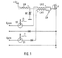
- the functional diagram of a conventional non-potential-free control circuit 1 shows a field-effect transistor F to be controlled - here as a MOS-FET formed - in the gate lead an inductor LH is arranged.
- the inductor LH is here as a pulse transformer with the partial inductors LH1 and LH2 trained.
- the control of the field effect transistor F takes place via a switch-on pulse, which is generated by the voltage of the Power supply source via the switch Si and the partial inductance LH1 the gate is switched (symbolized by Uein). Turning off the field effect transistor F takes place accordingly via the switch S2 and the partial inductance LH2.
- the switch-on and switch-off pulses for the field effect transistor F are, as shown schematically in Figure 1, mutually offset in phase, preferably by 180 degrees (push-pull pulses).
- Another inductance LN is coupled to the inductance LH in such a way that energy is fed back through it, in particular during the recharging process of the gate capacitance of the field effect transistor F is possible.
- the inductance LN with its winding sense (marked by circles in FIG. 1) with respect to the Windings of the inductors LH1 and LH2 arranged so that they serve as a discharge winding can work.
- the diode arranged in series is also corresponding DE poled.
- the voltage present at the gate of the field effect transistor F becomes therefore limited by the energy recovery via the discharge winding LN.
- the energy recovery takes place preferably for the voltage supply - in FIG 1 symbolized by Us - the gate control electronics.
- One of these control circuits similar drive circuit is disclosed in EP-A-0 534 013.
- the gate control according to the invention is potential-free by means of pulse transmitters realized.
- a configuration in this regard is shown in FIG Impulse transmission I1 and I2.
- the two switches S1 and S2 are connected in series the primary windings of these pulse transformers at the supply voltage Us of the control electronics.
- the respective secondary windings work - via the transistors T1 and T2 - on the inductors LH1 and LH2.
- Your Switching sections are operatively connected via the inductors LH1 and LH2 to the gate of the field effect transistor F.
- the one for switching on the field effect transistor F serving transistor T1 is tapped into the secondary winding of the pulse transmitter I1 controlled.
- the partial inductance IN serves to limit the gate voltage and Excess energy recovery.
- the discharge current can be used to control the Pulse transmission circuit can be used.
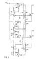
- the exemplary embodiment according to FIG. 3 shows a configuration for the control two field effect transistors F1 and F2 in a half-bridge circuit.
- switches S3 and S4 are separate pulse transmitters assigned to the cores K1 and K3 and the switch S5 a pulse transformer with the core K2 and two secondary windings W21 and W22.
- the for Switching off the field effect transistors F1 and F2 provided transistors T2 and T3 are the secondary windings W21 and W22 with their respective Switching sections connected in series.
Landscapes
- Engineering & Computer Science (AREA)
- Power Engineering (AREA)
- Electronic Switches (AREA)
- Power Conversion In General (AREA)
Description
Claims (6)
- Ansteuerschaltung für mindestens einen Feldeffekttransistor (F), mit mindestens einer Induktivität (LH) zur Strombegrenzung in einem Gate-Kreislauf des Feldeffekttransistors (F) über die der Feldeffekttransistor (F) mittels von Schaltern (S1, S2) erzeugten Impulsen, die eine zum Schalten des Feldeffekttransistors (F) notwendige Leistung enthalten, leitend bzw. sperrend gesteuert wird, wobei die Induktivität (LH) mit einer weiteren Induktivität (LN) so gekoppelt ist, daß über diese weitere Induktivität (LN) eine Energierückspeisung möglich ist, dadurch gekennzeichnet, daß der Gate-Kreislauf aus zwei Serienverbindungen besteht, die jeweils aus den Schaltstrecken eines Transistors (T1, T2), der Sekundärwicklung eines zwischen einen der Schalter (S1, S2) und einen der Transistoren (T1, T2) geschalteten Impulsüberträgers (I1, I2), einer Teilinduktivität (LH1, LH2) der Induktivität (LH) und der Gate-Source Strecke des Feldeffekttransistors (F) bestehen, wobei die Primärwicklungen der Impulsüberträger (11, 12) derart mit den Schaltern (S1, S2) verbunden sind, und die Steuer-Anschlüsse der Transistoren (T1, T2) derart mit den Sekundärwicklungen verbunden sind, daß die Transistoren (T1, T2) mittels der Schalter (S1, S2) im Gegentakt betrieben werden, und wobei die Impulsüberträger (11, 12) die zum Schalten des Feldeffekttransistors (F) notwendige Leistung übertragen.
- Ansteuerschaltung nach Anspruch 1, dadurch gekennzeichnet, daß die weitere Induktivität (LN) bezüglich ihres Wicklungssinnes und ihrer Beschaltung so angeordnet ist, daß die am Gate des Feldeffekttransistors (F) anliegende Spannung begrenzt werden kann.
- Ansteuerschaltung nach Anspruch 1 oder 2, dadurch gekennzeichnet, daß zumindest einer der Impulsübertrager (I1, I2) eine Anzapfung aufweist, wobei der Steuer-Anschluß des zugehörigen Transistors (T1) über diese Anzapfung mit der Sekundärwicklung des Impulsübertragers verbunden ist.
- Ansteuerschaltung nach einem der Ansprüche 1 bis 3, dadurch gekennzeichnet, daß sie für zwei in Halbbrückenschaltung angeordnete Feldeffekttransistoren (F1, F2) ausgelegt ist, wobei diese Feldeffekttransistoren (F1, F2) jeweils paarweise über Transistoren (T1, T2, T3, T4) mit zugehörigen Impulsübertragern (K1, K2, K3) gesteuert werden.
- Ansteuerschaltung nach Anspruch 4, dadurch gekennzeichnet, daß zum Einschalten der Transistoren (T1, T2, T3, T4) jeweils ein separater Impulsübertrager (K1, K3) vorgesehen ist und daß zum Ausschalten ein gemeinsamer Impulsübertrager (K2) vorgesehen ist.
- Ansteuerschaltung nach Anspruch 4, dadurch gekennzeichnet, daß für das Ein- und Ausschalten der Transistoren (T1, T2, T3, T4) insgesamt nur zwei Impulsübertrager (K1, K3) vorgesehen sind, deren Sekundärwicklungen jeweils auf ein Transistorpaar (T1, T2; T3, T4) arbeiten.
Applications Claiming Priority (3)
| Application Number | Priority Date | Filing Date | Title |
|---|---|---|---|
| DE19516138A DE19516138C1 (de) | 1995-05-03 | 1995-05-03 | Ansteuerschaltung für Feldeffekttransistoren |
| DE19516138 | 1995-05-03 | ||
| PCT/EP1996/001796 WO1996035260A1 (de) | 1995-05-03 | 1996-04-30 | Ansteuerschaltung für feldeffekttransistoren |
Publications (2)
| Publication Number | Publication Date |
|---|---|
| EP0824790A1 EP0824790A1 (de) | 1998-02-25 |
| EP0824790B1 true EP0824790B1 (de) | 2002-07-24 |
Family
ID=7760919
Family Applications (1)
| Application Number | Title | Priority Date | Filing Date |
|---|---|---|---|
| EP96914153A Expired - Lifetime EP0824790B1 (de) | 1995-05-03 | 1996-04-30 | Ansteuerschaltung für feldeffekttransistoren |
Country Status (3)
| Country | Link |
|---|---|
| EP (1) | EP0824790B1 (de) |
| DE (2) | DE19516138C1 (de) |
| WO (1) | WO1996035260A1 (de) |
Families Citing this family (1)
| Publication number | Priority date | Publication date | Assignee | Title |
|---|---|---|---|---|
| DE10306809A1 (de) * | 2003-02-18 | 2004-09-02 | Siemens Ag | Betrieb einer Halbbrücke, insbesondere einer Feldeffekttransistor-Halbbrücke |
Family Cites Families (8)
| Publication number | Priority date | Publication date | Assignee | Title |
|---|---|---|---|---|
| DE1257842B (de) * | 1966-05-13 | 1968-01-04 | Telefunken Patent | Saettigungsschutz fuer Schalttransistoren |
| US3940633A (en) * | 1974-07-01 | 1976-02-24 | General Electric Company | GTO turn-off circuit providing turn-off gate current pulse proportional to anode current |
| JPS5545276A (en) * | 1978-09-27 | 1980-03-29 | Hitachi Ltd | Gate circuit of gate turn-off thyristor |
| DE3413208A1 (de) * | 1984-04-07 | 1985-10-17 | Philips Patentverwaltung Gmbh, 2000 Hamburg | Schaltungsanordnung zum schalten eines stromes in einem transistor |
| US4873460A (en) * | 1988-11-16 | 1989-10-10 | California Institute Of Technology | Monolithic transistor gate energy recovery system |
| JPH03286619A (ja) * | 1990-04-02 | 1991-12-17 | Mitsubishi Electric Corp | 絶縁ゲート形半導体装置のゲート駆動回路および該回路を用いたフラッシュ制御装置 |
| US5134320A (en) * | 1991-03-07 | 1992-07-28 | Hughes Aircraft Company | High efficiency FET driver with energy recovery |
| DE69125280T2 (de) * | 1991-09-27 | 1997-08-14 | Alcatel Bell Sdt Sa | Verlustarmer Schwingkreis für Kapazitäts-Treiber |
-
1995
- 1995-05-03 DE DE19516138A patent/DE19516138C1/de not_active Expired - Fee Related
-
1996
- 1996-04-30 EP EP96914153A patent/EP0824790B1/de not_active Expired - Lifetime
- 1996-04-30 DE DE59609484T patent/DE59609484D1/de not_active Expired - Lifetime
- 1996-04-30 WO PCT/EP1996/001796 patent/WO1996035260A1/de not_active Ceased
Also Published As
| Publication number | Publication date |
|---|---|
| EP0824790A1 (de) | 1998-02-25 |
| WO1996035260A1 (de) | 1996-11-07 |
| DE19516138C1 (de) | 1996-12-19 |
| DE59609484D1 (de) | 2002-08-29 |
Similar Documents
| Publication | Publication Date | Title |
|---|---|---|
| EP1454389B1 (de) | Hochfrequenzanregungsanordnung | |
| DE69412414T2 (de) | Halbbrücken treiberschaltung | |
| DE19750168A1 (de) | Halbleitervorrichtung | |
| DE60101234T2 (de) | Schaltnetzteilgerät | |
| DE3603071A1 (de) | Gleichstrom-wechselstrom-wandler mit asymmetrischer halbbrueckenschaltung | |
| DE3914799A1 (de) | Durchflusswandler | |
| DE3912849C2 (de) | ||
| DE3741221C1 (de) | Anordnung zum Befreien eines Halbleiterschalters vor hoher Sperrspannungsbeanspruchung sowie Anwendung hierzu | |
| EP0982862A1 (de) | Widerstandsarme Bipolar-Brückenschaltung | |
| DE4011742C2 (de) | Gegentaktwechselrichter | |
| EP0679025A2 (de) | Schaltungsanordnung zum Einspeisen eines Antennensignals | |
| WO2022167192A1 (de) | Primärseitig seriell verschaltete sperrwandler mit klemmschaltung | |
| DE19516138C1 (de) | Ansteuerschaltung für Feldeffekttransistoren | |
| DE2411871B1 (de) | Schaltungsanordnung zur erdfreien Übertragung von Signalen über Trennstellen in Femmeldeanlagen | |
| EP2961049B1 (de) | Ansteuerschaltung eines Resonanzwandlers | |
| DE10027819A1 (de) | Gatetreiber mit Stromquelle für schnelle Thyristoren | |
| DE2719026A1 (de) | Schaltungsanordnung zur verringerung der ausschaltverluste in halbleiterschaltern | |
| DE3316281C2 (de) | Schaltnetzteil zur Gleichspannungswandlung | |
| DE2841342C2 (de) | Schaltungsanordnung zur Verringerung der Ausschaltverluste in Leistungs- Schalttransistoren | |
| DE4403908C1 (de) | Gegentaktschaltstufe | |
| WO1997044900A1 (de) | Schaltnetzgerät | |
| EP0581109B1 (de) | Schaltungsanordnung zum Ansteuern eines in einem Abwärtswandler angeordneten Schaltelements | |
| DE3241821C2 (de) | ||
| EP0684687A1 (de) | Gleichspannungskonverter | |
| AT504121B1 (de) | Schaltungsanordnung zur ansteuerung von schalttransistoren |
Legal Events
| Date | Code | Title | Description |
|---|---|---|---|
| PUAI | Public reference made under article 153(3) epc to a published international application that has entered the european phase |
Free format text: ORIGINAL CODE: 0009012 |
|
| 17P | Request for examination filed |
Effective date: 19971030 |
|
| AK | Designated contracting states |
Kind code of ref document: A1 Designated state(s): DE FR GB IT NL |
|
| 17Q | First examination report despatched |
Effective date: 19980213 |
|
| GRAG | Despatch of communication of intention to grant |
Free format text: ORIGINAL CODE: EPIDOS AGRA |
|
| GRAG | Despatch of communication of intention to grant |
Free format text: ORIGINAL CODE: EPIDOS AGRA |
|
| GRAH | Despatch of communication of intention to grant a patent |
Free format text: ORIGINAL CODE: EPIDOS IGRA |
|
| RAP1 | Party data changed (applicant data changed or rights of an application transferred) |
Owner name: TELDIX GMBH |
|
| GRAH | Despatch of communication of intention to grant a patent |
Free format text: ORIGINAL CODE: EPIDOS IGRA |
|
| GRAA | (expected) grant |
Free format text: ORIGINAL CODE: 0009210 |
|
| AK | Designated contracting states |
Kind code of ref document: B1 Designated state(s): DE FR GB IT NL |
|
| PG25 | Lapsed in a contracting state [announced via postgrant information from national office to epo] |
Ref country code: NL Free format text: LAPSE BECAUSE OF FAILURE TO SUBMIT A TRANSLATION OF THE DESCRIPTION OR TO PAY THE FEE WITHIN THE PRESCRIBED TIME-LIMIT Effective date: 20020724 Ref country code: IT Free format text: LAPSE BECAUSE OF FAILURE TO SUBMIT A TRANSLATION OF THE DESCRIPTION OR TO PAY THE FEE WITHIN THE PRESCRIBED TIME-LIMIT;WARNING: LAPSES OF ITALIAN PATENTS WITH EFFECTIVE DATE BEFORE 2007 MAY HAVE OCCURRED AT ANY TIME BEFORE 2007. THE CORRECT EFFECTIVE DATE MAY BE DIFFERENT FROM THE ONE RECORDED. Effective date: 20020724 |
|
| REG | Reference to a national code |
Ref country code: GB Ref legal event code: FG4D Free format text: NOT ENGLISH |
|
| REF | Corresponds to: |
Ref document number: 59609484 Country of ref document: DE Date of ref document: 20020829 |
|
| GBT | Gb: translation of ep patent filed (gb section 77(6)(a)/1977) |
Effective date: 20021024 |
|
| ET | Fr: translation filed | ||
| NLV1 | Nl: lapsed or annulled due to failure to fulfill the requirements of art. 29p and 29m of the patents act | ||
| PLBE | No opposition filed within time limit |
Free format text: ORIGINAL CODE: 0009261 |
|
| STAA | Information on the status of an ep patent application or granted ep patent |
Free format text: STATUS: NO OPPOSITION FILED WITHIN TIME LIMIT |
|
| 26N | No opposition filed |
Effective date: 20030425 |
|
| PGFP | Annual fee paid to national office [announced via postgrant information from national office to epo] |
Ref country code: GB Payment date: 20140423 Year of fee payment: 19 |
|
| PGFP | Annual fee paid to national office [announced via postgrant information from national office to epo] |
Ref country code: FR Payment date: 20140416 Year of fee payment: 19 Ref country code: DE Payment date: 20140429 Year of fee payment: 19 |
|
| REG | Reference to a national code |
Ref country code: DE Ref legal event code: R119 Ref document number: 59609484 Country of ref document: DE |
|
| GBPC | Gb: european patent ceased through non-payment of renewal fee |
Effective date: 20150430 |
|
| PG25 | Lapsed in a contracting state [announced via postgrant information from national office to epo] |
Ref country code: GB Free format text: LAPSE BECAUSE OF NON-PAYMENT OF DUE FEES Effective date: 20150430 Ref country code: DE Free format text: LAPSE BECAUSE OF NON-PAYMENT OF DUE FEES Effective date: 20151103 |
|
| REG | Reference to a national code |
Ref country code: FR Ref legal event code: ST Effective date: 20151231 |
|
| PG25 | Lapsed in a contracting state [announced via postgrant information from national office to epo] |
Ref country code: FR Free format text: LAPSE BECAUSE OF NON-PAYMENT OF DUE FEES Effective date: 20150430 |