EP0823719B1 - Solid electrolytic capacitor having pre-plated lead terminals and manufacturing process thereof - Google Patents
Solid electrolytic capacitor having pre-plated lead terminals and manufacturing process thereof Download PDFInfo
- Publication number
- EP0823719B1 EP0823719B1 EP97112365A EP97112365A EP0823719B1 EP 0823719 B1 EP0823719 B1 EP 0823719B1 EP 97112365 A EP97112365 A EP 97112365A EP 97112365 A EP97112365 A EP 97112365A EP 0823719 B1 EP0823719 B1 EP 0823719B1
- Authority
- EP
- European Patent Office
- Prior art keywords
- plating
- pulse
- lead terminals
- plating layer
- plated
- Prior art date
- Legal status (The legal status is an assumption and is not a legal conclusion. Google has not performed a legal analysis and makes no representation as to the accuracy of the status listed.)
- Expired - Lifetime
Links
Images


Classifications
-
- H—ELECTRICITY
- H01—ELECTRIC ELEMENTS
- H01G—CAPACITORS; CAPACITORS, RECTIFIERS, DETECTORS, SWITCHING DEVICES OR LIGHT-SENSITIVE DEVICES, OF THE ELECTROLYTIC TYPE
- H01G9/00—Electrolytic capacitors, rectifiers, detectors, switching devices, light-sensitive or temperature-sensitive devices; Processes of their manufacture
- H01G9/004—Details
- H01G9/008—Terminals
- H01G9/012—Terminals specially adapted for solid capacitors
-
- C—CHEMISTRY; METALLURGY
- C25—ELECTROLYTIC OR ELECTROPHORETIC PROCESSES; APPARATUS THEREFOR
- C25D—PROCESSES FOR THE ELECTROLYTIC OR ELECTROPHORETIC PRODUCTION OF COATINGS; ELECTROFORMING; APPARATUS THEREFOR
- C25D5/00—Electroplating characterised by the process; Pretreatment or after-treatment of workpieces
- C25D5/18—Electroplating using modulated, pulsed or reversing current
-
- H—ELECTRICITY
- H01—ELECTRIC ELEMENTS
- H01G—CAPACITORS; CAPACITORS, RECTIFIERS, DETECTORS, SWITCHING DEVICES OR LIGHT-SENSITIVE DEVICES, OF THE ELECTROLYTIC TYPE
- H01G9/00—Electrolytic capacitors, rectifiers, detectors, switching devices, light-sensitive or temperature-sensitive devices; Processes of their manufacture
- H01G9/15—Solid electrolytic capacitors
-
- H—ELECTRICITY
- H01—ELECTRIC ELEMENTS
- H01L—SEMICONDUCTOR DEVICES NOT COVERED BY CLASS H10
- H01L2224/00—Indexing scheme for arrangements for connecting or disconnecting semiconductor or solid-state bodies and methods related thereto as covered by H01L24/00
- H01L2224/01—Means for bonding being attached to, or being formed on, the surface to be connected, e.g. chip-to-package, die-attach, "first-level" interconnects; Manufacturing methods related thereto
- H01L2224/26—Layer connectors, e.g. plate connectors, solder or adhesive layers; Manufacturing methods related thereto
- H01L2224/31—Structure, shape, material or disposition of the layer connectors after the connecting process
- H01L2224/32—Structure, shape, material or disposition of the layer connectors after the connecting process of an individual layer connector
- H01L2224/321—Disposition
- H01L2224/32151—Disposition the layer connector connecting between a semiconductor or solid-state body and an item not being a semiconductor or solid-state body, e.g. chip-to-substrate, chip-to-passive
- H01L2224/32221—Disposition the layer connector connecting between a semiconductor or solid-state body and an item not being a semiconductor or solid-state body, e.g. chip-to-substrate, chip-to-passive the body and the item being stacked
- H01L2224/32245—Disposition the layer connector connecting between a semiconductor or solid-state body and an item not being a semiconductor or solid-state body, e.g. chip-to-substrate, chip-to-passive the body and the item being stacked the item being metallic
Definitions
- the present invention relates to a resin-molded electronic component having lead terminals, and more particularly, to a chip type solid electrolyte capacitor having solder plated lead terminals, and a process for manufacturing the same.
- the chip type component such as a solid electrolyte capacitor featuring a small size and high capacity has enjoyed an increasingly expanded market scale and is used in various applications.
- a chip type solid electrolyte capacitor has a capacitor element 1 having a cathode layer 3, an anode lead 2, an anode lead terminal 8 connected to the anode lead 2 by welding or the like, and a cathode lead terminal 9 connected to the cathode layer 3.
- the cathode layer 3 and the cathode lead terminal 9 are connected by a conductive adhesive 10 such as silver paste.
- the capacitor is packaged by resin 6, leaving portions of the anode and cathode lead terminals 8 and 9 exposed.
- the anode and cathode lead terminals 8 and 9 are bent along the outer surface of the resin package 6. Since these lead terminals 8 and 9 are pre-plated with a plating layer of solder or the like by a direct current plating method using a linear current waveform as shown in Fig.9, it has the following disadvantages (1) and (2).
- Patents Abstracts of Japan, vol. 95, no. 11, & JP 07 202100 A discloses a method of plating lead parts of a semiconductor device, in which alternately positive pulse currents and negative pulse currents having absolute values which are smaller than those of the positive pulse currents are supplied. By this means plated films with nearly constant thickness over the whole lead parts are obtained.
- the above objective of the present invention is achieved by employing electroplated lead terminals which contain organic substances in an amount of 0.03 wt % or less.
- a pre-plated anode lead terminal is welded to an anode lead of a capacitor element and pre-plated cathode lead terminal is connected to a cathode layer of the capacitor element by using a conductive adhesive.
- the capacitor element is encapsulated by an insulating member so as to leave a portion of anode and cathode lead terminals exposed. Both of the encapsulated and exposed portions of the pre-plated anode and cathode lead terminals have a pre-plated layer containing organic substances in an amount of 0.03 wt.% or less.
- Such a small amount of the organic substances in the electroplated layer can be achieved by using a special puls plating method with a current waveform having a counter pulse.
- ON time and OFF time of the current waveform is selected to be about 10 to 500 msec and the OFF time includes a counter (negative) current pulse which has an amplitude that is from 1/2 to 1/50 that of the ON time pulse and a duration of 2 to 20 msec.
- Fig. 1 is a side cross sectional view of a chip type solid electrolyte capacitor according to an embodiment of the present invention.
- Fig. 2A is a perspective view of a chip type solid electrolyte capacitor assembled in a lead frame prior to a molding prosess.
- Fig. 2B is an enlarged perspective view showing a main part B shown in Fig. 2A.
- Fig. 3 is a waveform diagram showing an example of the current waveform used in the pulse plating method of the present invention.
- Fig. 4 is a waveform diagram showing an example of the current waveform used in a preferred embodiment of the present invention.
- Fig. 5 is a diagram of a plating apparatus for use in the present invention.
- Fig. 6 is a graph correlating impurity content of the plating layer and cathode connection strength.
- Fig. 7 is a graph showing the rate of solder ball generation as a function of impurity content.
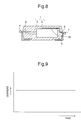
- Fig. 8 is a side cross sectional view of an example of a conventional chip type solid electrolyte capacitor.
- Fig. 9 is a waveform diagram showing an example of the current waveform used in a conventional direct current plating method.
- an anode body of a valve metal such as tantalum is subjected to anodic oxidation and a solid electrolyte layer such as manganese oxide layer, a carbon layer and a silver paste layer are formed thereon sequentially.
- a solid electrolyte capacitor element 1 having a cathode layer 3 in the outer-most layer is formed.
- anode lead 2 embedded in this capacitor element 1 and a pre-plated anode lead terminal 8 are connected together by means of welding or the like.
- a pre-plated cathode lead terminal 9 is connected to the cathode layer 3 via a conductive adhesive 10.
- the assembly is thereafter encapsulated with an electrically insulating member 6 such as epoxy resin by means of transfer molding process such that a portion of each of the anode and cathode lead terminals 8 and 9 is exposed.
- solder plating may be carried out for the lead frame after punching out from a non-plated metal tape. In that case, whole surfaces of the lead frame is coated with a plating layer.
- the solder plating layer of the present invention is formed using a pulse plating method with a current waveform having an ON time of from about 10 to about 500 msec including a positive current pulse and an OFF time of from about 10 msec to about 500 msec including a negative current pulse as shown in Fig. 3.
- the negative current pulse (counter pulse) has an amplitude that is from 1/2 - 1/50 that of the positive current pulse and a duration of from 2 to 20 msec.
- Other than the counter pulse preferably, there is no current flow during the OFF portion of the waveform.
- the timing of the negative current pulse is not restricted to the position shown in Fig. 3, but may be at any position between adjacent positive current pulses.
- the current waveform has an ON time (positive pulse) of 200 msec and an OFF time of 200 msec including a 10 msec negative pulse at the trailing edge of the positive pulse as shown in Fig. 4.
- the amplitude of the negative pulse is selected to be 1/10 of the positive pulse.
- the pulse plating method of the present invention reduces the amount of organic substances (e.g., dispersant and/or brightener) from the solder plating layer having a thickness of about 4 ⁇ m.
- a well known plating apparatus can be used for this invention as shown in Fig. 5, including plating bath 13, electrode 14, lead terminal base metal 15 and current source 16.
- the base metal 15 may be grounded.
- the electrode 14 is made of Pb/Sn alloy and solder plating bath contains 10 to 60 vol.-% of Sn(BF 4 ) 2 , 1 to 40 vol.-% of Pb(BF 4 ) 2 , 10 to 70 vol.-% of HBF 4 and 1 to 20 vol.-% of additives.
- the base metal 15 is made of well known 42-alloy which is widely used for lead terminals of electronic components. Needless to say, the solder plating bath is not restricted to the above described solution, for example, the solder plating solution disclosed in U.S. Patent No. 4,589,962 may be used.
- connection strength between the cathode layer 3 and the cathode lead terminal 9 of the chip type solid electrolyte capacitor thus prepared prior to forming the external package was evaluated.
- the present inventors found, as shown in Fig. 6, that the connection strength in the present invention was about 1.5 times that of a conventional device.
- the fluctuation in connection strength was also reduced by 20 % or more.
- solder balls were generated 75 % of the time (75 % solder ball generation rate) when the cathode lead terminal had a solder layer thereon formed using a conventional direct current plating method, while no solder balls were generated in making the solid electrolyte capacitor of the present invention.
- solder balls substantially do not form when the organic substance (impurity) content in the solder plating layer is 0.03 wt.-% or less.
- This effect is obtained by providing a plating layer on all of the surfaces of the anode and cathode lead terminals or by providing only upper plating layer 91 of the anode and cathode lead terminals 8 and 9, which surface is subsequently soldered to a printed wiring board.
- the content of organic substances (impurities) contained in a plating layer formed on the anode and cathode lead terminals in a conventional direct current plating method is about 0.2 wt.-%.
- the impurity content can be reduced when the component is subjected to thermal mounting stress and a solder ball is not formed.
- Japanese Patent Application Laid-Open No. 62-151592 shows to apply a pulsative current of 1 msec ON time and 25-35 msec OFF time to plating electrodes to form a defectless noble metal plating layer.
- plating layer still contains organic substances in an amount of 0.05 wt.-% - 0.08 wt.-%.
- Japanese Patent Application Laid-Open No. 63-95698 shows a solder plating method for obtaining a uniform plated solder layer on both of conductive circuit pattern and throughhole of a multilayer printed wiring board.
- a counter pulse is applied to the plating electrodes, there is no mention about the organic substances in the plating layer. Since the pulse width is selected to be 4.0 msec on less without OFF time and both of the positive and negative pulses have the same amplitude, it is unknown whether the amount of the organic substances in the plating layer is less than 0.03 wt.-% or not . Even if the amount of the organic substances could be less than 0.03 wt.-%, it does not anticipate the present invention because the Japanese Patent Application Laid-Open No.
- the following advantages are realized by plating the anode and cathode lead terminals with a layer of solder or the like using the pulse plating method of the present invention.
Description
- The present invention relates to a resin-molded electronic component having lead terminals, and more particularly, to a chip type solid electrolyte capacitor having solder plated lead terminals, and a process for manufacturing the same.
- As the weight and size of electronic equipment is progressively reduced, and as surface mounting technology has advanced, the chip type component such as a solid electrolyte capacitor featuring a small size and high capacity has enjoyed an increasingly expanded market scale and is used in various applications.
- Conventionally, as shown in Fig. 8, a chip type solid electrolyte capacitor has a
capacitor element 1 having acathode layer 3, ananode lead 2, ananode lead terminal 8 connected to theanode lead 2 by welding or the like, and acathode lead terminal 9 connected to thecathode layer 3. - Moreover, the
cathode layer 3 and thecathode lead terminal 9 are connected by aconductive adhesive 10 such as silver paste. The capacitor is packaged byresin 6, leaving portions of the anode andcathode lead terminals cathode lead terminals resin package 6. Since theselead terminals - (1) Organic components contained in a plating solution
such as a brightener or dispersant are incorporated into the
plating layer. As a result, the plating layer of solder or the
like formed on the anode and
cathode lead terminals - Sample:
- Plating film formed by direct current plating
- Detected components:
- Dichlorotoluene, N,N,2,6-tetramethylbenzeneamine, trichlorobenzene, chlorobenzenemethanol, dichlorobenzaldehyde, dichlorobenzenemethanol, lauric acid methyl
conductive adhesive 10 and thecathode lead terminal 9 affects connection reliability, and reduces the connection strength between theconductive adhesive 10 and thecathode lead terminal 9. In the worst case, the cathode lead terminal may peel off to result in an electrically open circuit. - (2) The plated solder on the
lead terminals resin package 6 tends to elute from the resin package to formsolder balls 7. This occurs when an excessive amount of an organic substance is generated due to thermal stress in mounting the electronic component. The resultingsolder ball 7 can short circuit conductive patterns when the component is mounted on a printed circuit board. -
- To avoid the foregoing disadvantages, it is possible to plate only the exposed portion of the lead terminals. But such selective plating increases a production cost.
- Patents Abstracts of Japan, vol. 95, no. 11, & JP 07 202100 A (Yamaha Corporation) discloses a method of plating lead parts of a semiconductor device, in which alternately positive pulse currents and negative pulse currents having absolute values which are smaller than those of the positive pulse currents are supplied. By this means plated films with nearly constant thickness over the whole lead parts are obtained.
- It is therefore an object of the present invention to provide an electronic component such as a solid electrolyte capacitor which maintains good connection reliability at its connecting portion using conductive adhesive and prevents the generation of a solder ball, and a process for manufacturing the same without resorting to a selective plating method.
- According to the present invention the above object is achieved by a solid electrolyte capacitor according to
claim 1 and a process for manufacturing the same according to claim 4; the dependent claims are related to further advantageous aspects of the invention. - The above objective of the present invention is achieved by employing electroplated lead terminals which contain organic substances in an amount of 0.03 wt % or less. In the case of a solid electrolyte capacitor, a pre-plated anode lead terminal is welded to an anode lead of a capacitor element and pre-plated cathode lead terminal is connected to a cathode layer of the capacitor element by using a conductive adhesive. The capacitor element is encapsulated by an insulating member so as to leave a portion of anode and cathode lead terminals exposed. Both of the encapsulated and exposed portions of the pre-plated anode and cathode lead terminals have a pre-plated layer containing organic substances in an amount of 0.03 wt.% or less.
- Such a small amount of the organic substances in the electroplated layer can be achieved by using a special puls plating method with a current waveform having a counter pulse. ON time and OFF time of the current waveform is selected to be about 10 to 500 msec and the OFF time includes a counter (negative) current pulse which has an amplitude that is from 1/2 to 1/50 that of the ON time pulse and a duration of 2 to 20 msec.
- Fig. 1 is a side cross sectional view of a chip type solid electrolyte capacitor according to an embodiment of the present invention.
- Fig. 2A is a perspective view of a chip type solid electrolyte capacitor assembled in a lead frame prior to a molding prosess.
- Fig. 2B is an enlarged perspective view showing a main part B shown in Fig. 2A.
- Fig. 3 is a waveform diagram showing an example of the current waveform used in the pulse plating method of the present invention.
- Fig. 4 is a waveform diagram showing an example of the current waveform used in a preferred embodiment of the present invention.
- Fig. 5 is a diagram of a plating apparatus for use in the present invention.
- Fig. 6 is a graph correlating impurity content of the plating layer and cathode connection strength.
- Fig. 7 is a graph showing the rate of solder ball generation as a function of impurity content.
- Fig. 8 is a side cross sectional view of an example of a conventional chip type solid electrolyte capacitor.
- Fig. 9 is a waveform diagram showing an example of the current waveform used in a conventional direct current plating method.
- Referring to Fig. 1, an anode body of a valve metal such as tantalum is subjected to anodic oxidation and a solid electrolyte layer such as manganese oxide layer, a carbon layer and a silver paste layer are formed thereon sequentially. As a result, a solid
electrolyte capacitor element 1 having acathode layer 3 in the outer-most layer is formed. As shown in Fig. 2A,anode lead 2 embedded in thiscapacitor element 1 and a pre-platedanode lead terminal 8 are connected together by means of welding or the like. A pre-platedcathode lead terminal 9 is connected to thecathode layer 3 via aconductive adhesive 10. The assembly is thereafter encapsulated with an electrically insulatingmember 6 such as epoxy resin by means of transfer molding process such that a portion of each of the anode andcathode lead terminals - Since a
lead frame 900 is punched out from a solder-plated metal tape (not shown),lead terminals solder plating layer 91 and bottom solder plating layer 92 and side edges thereof are not plated as shown in Fig. 2B. Needless to say, solder plating may be carried out for the lead frame after punching out from a non-plated metal tape. In that case, whole surfaces of the lead frame is coated with a plating layer. - The solder plating layer of the present invention is formed using a pulse plating method with a current waveform having an ON time of from about 10 to about 500 msec including a positive current pulse and an OFF time of from about 10 msec to about 500 msec including a negative current pulse as shown in Fig. 3. The negative current pulse (counter pulse) has an amplitude that is from 1/2 - 1/50 that of the positive current pulse and a duration of from 2 to 20 msec. Other than the counter pulse, preferably, there is no current flow during the OFF portion of the waveform. The timing of the negative current pulse is not restricted to the position shown in Fig. 3, but may be at any position between adjacent positive current pulses.
- In a preferred embodiment, the current waveform has an ON time (positive pulse) of 200 msec and an OFF time of 200 msec including a 10 msec negative pulse at the trailing edge of the positive pulse as shown in Fig. 4. The amplitude of the negative pulse is selected to be 1/10 of the positive pulse. The pulse plating method of the present invention reduces the amount of organic substances (e.g., dispersant and/or brightener) from the solder plating layer having a thickness of about 4µm.
- A well known plating apparatus can be used for this invention as shown in Fig. 5, including
plating bath 13,electrode 14, leadterminal base metal 15 andcurrent source 16. When positive and negative pulses are applied to theelectrode 14, thebase metal 15 may be grounded. Theelectrode 14 is made of Pb/Sn alloy and solder plating bath contains 10 to 60 vol.-% of Sn(BF4)2, 1 to 40 vol.-% of Pb(BF4)2, 10 to 70 vol.-% of HBF4 and 1 to 20 vol.-% of additives. Thebase metal 15 is made of well known 42-alloy which is widely used for lead terminals of electronic components. Needless to say, the solder plating bath is not restricted to the above described solution, for example, the solder plating solution disclosed in U.S. Patent No. 4,589,962 may be used. - The connection strength between the
cathode layer 3 and thecathode lead terminal 9 of the chip type solid electrolyte capacitor thus prepared prior to forming the external package was evaluated. The present inventors found, as shown in Fig. 6, that the connection strength in the present invention was about 1.5 times that of a conventional device. The fluctuation in connection strength was also reduced by 20 % or more. - In addition, the product was conveyed into a heat furnace after the external package was formed to apply thermal stress thereon and inspected for solder ball generation. It was found that solder balls were generated 75 % of the time (75 % solder ball generation rate) when the cathode lead terminal had a solder layer thereon formed using a conventional direct current plating method, while no solder balls were generated in making the solid electrolyte capacitor of the present invention.
- Furthermore, as clearly seen from the relationship between the cathode connection strength and the impurity content wt.-% as shown in Fig. 7, the present inventors found that solder balls substantially do not form when the organic substance (impurity) content in the solder plating layer is 0.03 wt.-% or less.
- This effect is obtained by providing a plating layer on all of the surfaces of the anode and cathode lead terminals or by providing only
upper plating layer 91 of the anode andcathode lead terminals - The content of organic substances (impurities) contained in a plating layer formed on the anode and cathode lead terminals in a conventional direct current plating method is about 0.2 wt.-%. On the other hand, in the pulse plating method of the present invention, the impurity content can be reduced when the component is subjected to thermal mounting stress and a solder ball is not formed.
- Although a simple pulse plating method is known to provide a uniform plating layer. For example, Japanese Patent Application Laid-Open No. 62-151592 shows to apply a pulsative current of 1 msec ON time and 25-35 msec OFF time to plating electrodes to form a defectless noble metal plating layer. However, since the ON time is very short and no counter pulse is provided during the OFF time, plating layer still contains organic substances in an amount of 0.05 wt.-% - 0.08 wt.-%.
- On the other hand, Japanese Patent Application Laid-Open No. 63-95698 shows a solder plating method for obtaining a uniform plated solder layer on both of conductive circuit pattern and throughhole of a multilayer printed wiring board. Although a counter pulse is applied to the plating electrodes, there is no mention about the organic substances in the plating layer. Since the pulse width is selected to be 4.0 msec on less without OFF time and both of the positive and negative pulses have the same amplitude, it is unknown whether the amount of the organic substances in the plating layer is less than 0.03 wt.-% or not . Even if the amount of the organic substances could be less than 0.03 wt.-%, it does not anticipate the present invention because the Japanese Patent Application Laid-Open No. 63-95698 does not mention about the solid electrolyte capacitor and its solder plated lead terminals connected to the cathode layer by using a conductive adhesive, much less the problems of generation of gas and solder ball which is peculiar to the molded-type electronic components having a pre-plated lead terminals passing through the molded package thereof.
- As described above, the following advantages are realized by plating the anode and cathode lead terminals with a layer of solder or the like using the pulse plating method of the present invention.
- (1) Because organic substances such as a brightener and/or dispersant normally contained in the plating solution are not incorporated into the plating layer, differing from the case where solder is plated by a direct current plating method, the plating layer formed on the anode and cathode lead terminals has a low organic substance content. Thus, hardly any gas is generated in the adhering interface between the conductive adhesive and the cathode lead terminal due to thermal stress when mounting the finished electronic component. As a result, the connection reliabilty is enhanced.
- (2) In addition, it is possible to eliminate the problem of solder ball generation.
-
- It should further be apparent to those skilled in the art that various changes in form and detail of the invention as shown and described above may be made. It is intended that such changes be included within the scope of the claims appended hereto.
Claims (7)
- A solid electrolyte capacitor comprising:a capacitor element (1), pre-plated anode and cathode lead terminals (8, 9) wherein said anode lead terminal (8) is welded to an anode lead (2) of said capacitor element and said cathode lead terminal (9) is connected to a cathode layer (3) of said capacitor element via a conductive adhesive (10); andan insulating member (6) encapsulating said capacitor element (1) and leaving a portion of said lead terminals (8, 9) exposed, said pre-plated lead terminals (8) having a plating layer (91) containing organic substances in an amount of 0.03 wt.-% or less, said plating layer being formed by using a pulse plating method comprising pulse plating with a current waveform having a counter pulse.
- The capacitor electronic as claimed in claim 1, wherein said plating layer comprises a solder plating layer.
- The capacitor as claimed in claim 1, wherein said plating layer (91) is present only on an upper and a lower surface of said anode and cathode lead terminals.
- A process for manufacturing a solid electrolyte capacitor comprising:forming pre-plated anode and cathode lead terminals (8, 9) having a plating layer (91) containing organic substances in an amount of 0.03 wt.-% or less using a pulse plating method comprising pulse plating with a current waveform having a counter pulse;providing a capacitor element (1);welding said pre-plated anode lead terminal (8) to an anode lead (2) of said capacitor element (1) and connecting said cathode lead terminal (9) to a cathode layer (3) of said capacitor element via a conductive adhesive (10); andencapsulating said capacitor element (1) while leaving a portion of said pre-plated lead terminal (8, 9) exposed.
- The process as claimed in claim 4, wherein said current wave-form has an ON time of from 10 to 500 msec including a positive current pulse, an OFF time of from 10 msec to 500 msec including a counter pulse, and the counter pulse is a negative current pulse having an amplitude that is from ½ - 1/50 that of the positive current pulse and a duration of from 2 to 20 msec.
- The process as claimed in claim 4, wherein said step of forming a plating layer (91) comprises providing an electrolytic plating bath and a pulsating current source, immersing a lead terminal base metal in said plating bath and passing a pulsating current having a counter pulse through said plating bath.
- The process as claimed in claim 4, wherein said step of forming a plating layer (91) comprises plating a metal sheet and punching the metal sheet to obtain pre-plated lead terminals having a plating layer present only on an upper surface and a lower surface of said lead terminals.
Applications Claiming Priority (3)
| Application Number | Priority Date | Filing Date | Title |
|---|---|---|---|
| JP19790196 | 1996-07-26 | ||
| JP197901/96 | 1996-07-26 | ||
| JP19790196 | 1996-07-26 |
Publications (2)
| Publication Number | Publication Date |
|---|---|
| EP0823719A1 EP0823719A1 (en) | 1998-02-11 |
| EP0823719B1 true EP0823719B1 (en) | 2002-06-05 |
Family
ID=16382172
Family Applications (1)
| Application Number | Title | Priority Date | Filing Date |
|---|---|---|---|
| EP97112365A Expired - Lifetime EP0823719B1 (en) | 1996-07-26 | 1997-07-18 | Solid electrolytic capacitor having pre-plated lead terminals and manufacturing process thereof |
Country Status (5)
| Country | Link |
|---|---|
| US (2) | US6127205A (en) |
| EP (1) | EP0823719B1 (en) |
| KR (1) | KR100279861B1 (en) |
| CN (1) | CN1115084C (en) |
| DE (1) | DE69712999T2 (en) |
Families Citing this family (14)
| Publication number | Priority date | Publication date | Assignee | Title |
|---|---|---|---|---|
| US6324051B1 (en) | 1999-10-29 | 2001-11-27 | Matsushita Electric Industrial Co., Ltd. | Solid electrolytic capacitor |
| DE10058622A1 (en) * | 2000-11-15 | 2002-05-29 | Vishay Semiconductor Gmbh | Molded electronic component |
| DE10058608A1 (en) | 2000-11-25 | 2002-05-29 | Vishay Semiconductor Gmbh | Conductor strip arrangement for a molded electronic component and method for molding |
| US6723957B2 (en) * | 2002-03-29 | 2004-04-20 | Illinois Tool Works Inc. | Method and apparatus for welding |
| DE10222405B4 (en) * | 2002-05-21 | 2007-09-27 | Epcos Ag | Chip capacitor and method for its production |
| JP2006518553A (en) * | 2003-02-19 | 2006-08-10 | ハネウエル・インターナシヨナル・インコーポレーテツド | Method of generating thermal interconnect system and use thereof |
| WO2006077906A1 (en) * | 2005-01-24 | 2006-07-27 | Matsushita Electric Industrial Co., Ltd. | Chip type solid electrolytic capacitor |
| DE102005005095A1 (en) * | 2005-02-04 | 2006-08-10 | Höllmüller Maschinenbau GmbH | Process and device for the electrochemical treatment of components in continuous flow systems |
| CN100370562C (en) * | 2005-02-05 | 2008-02-20 | 西安交通大学 | Method for producing solid sheet type electrolytic capacitor |
| US20090237865A1 (en) * | 2005-11-01 | 2009-09-24 | Showa Denko K.K. | Solid electrolytic capacitor and method for manufacturing same |
| US8102668B2 (en) * | 2008-05-06 | 2012-01-24 | International Rectifier Corporation | Semiconductor device package with internal device protection |
| JP5274308B2 (en) * | 2009-03-03 | 2013-08-28 | 三洋電機株式会社 | Solid electrolytic capacitor |
| US9070392B1 (en) | 2014-12-16 | 2015-06-30 | Hutchinson Technology Incorporated | Piezoelectric disk drive suspension motors having plated stiffeners |
| WO2017003782A1 (en) | 2015-06-30 | 2017-01-05 | Hutchinson Technology Incorporated | Disk drive head suspension structures having improved gold-dielectric joint reliability |
Family Cites Families (13)
| Publication number | Priority date | Publication date | Assignee | Title |
|---|---|---|---|---|
| CH494824A (en) * | 1969-07-10 | 1970-08-15 | Fluehmann Werner | Process for the electrodeposition of copper with high ductility |
| US3650232A (en) * | 1970-09-08 | 1972-03-21 | Amp Inc | Method and apparatus for manufacturing lead frames |
| JPS547267B2 (en) * | 1973-09-21 | 1979-04-05 | ||
| US3983014A (en) * | 1974-12-16 | 1976-09-28 | The Scionics Corporation | Anodizing means and techniques |
| AU533310B2 (en) * | 1980-12-27 | 1983-11-17 | K.K. Chiyoda | Chemically producing anodic oxidation coat on al or al alloy |
| US4666567A (en) * | 1981-07-31 | 1987-05-19 | The Boeing Company | Automated alternating polarity pulse electrolytic processing of electrically conductive substances |
| JPS6152388A (en) * | 1984-08-17 | 1986-03-15 | Sony Corp | Plating device |
| US4589962A (en) * | 1985-06-03 | 1986-05-20 | National Semiconductor Corporation | Solder plating process and semiconductor product |
| US4631116A (en) * | 1985-06-05 | 1986-12-23 | Hughes Aircraft Company | Method of monitoring trace constituents in plating baths |
| JPS62151592A (en) * | 1985-12-25 | 1987-07-06 | Hitachi Cable Ltd | Production of gold plated lead frame |
| JPS6395698A (en) * | 1986-10-09 | 1988-04-26 | 富士通株式会社 | Method of solder plating of multilayer printed board |
| JPH02243791A (en) * | 1989-03-15 | 1990-09-27 | Hitachi Cable Ltd | Solder plating method |
| JPH07202100A (en) * | 1993-12-28 | 1995-08-04 | Yamaha Corp | Method of plating lead part of semiconductor device |
-
1997
- 1997-07-18 DE DE69712999T patent/DE69712999T2/en not_active Expired - Lifetime
- 1997-07-18 EP EP97112365A patent/EP0823719B1/en not_active Expired - Lifetime
- 1997-07-24 KR KR1019970034675A patent/KR100279861B1/en not_active IP Right Cessation
- 1997-07-25 US US08/901,239 patent/US6127205A/en not_active Expired - Lifetime
- 1997-07-25 CN CN97116703A patent/CN1115084C/en not_active Expired - Fee Related
-
2000
- 2000-08-17 US US09/639,821 patent/US6294826B1/en not_active Expired - Lifetime
Also Published As
| Publication number | Publication date |
|---|---|
| US6127205A (en) | 2000-10-03 |
| KR980013559A (en) | 1998-04-30 |
| EP0823719A1 (en) | 1998-02-11 |
| CN1175881A (en) | 1998-03-11 |
| DE69712999D1 (en) | 2002-07-11 |
| CN1115084C (en) | 2003-07-16 |
| DE69712999T2 (en) | 2003-01-23 |
| KR100279861B1 (en) | 2001-02-01 |
| US6294826B1 (en) | 2001-09-25 |
Similar Documents
| Publication | Publication Date | Title |
|---|---|---|
| EP0823719B1 (en) | Solid electrolytic capacitor having pre-plated lead terminals and manufacturing process thereof | |
| US6919137B2 (en) | High-strength solder joint | |
| KR101026586B1 (en) | Leadframes for improved moisture reliability and enhanced solderability of semiconductor devices | |
| US20060001132A1 (en) | Palladium-spot leadframes for high adhesion semiconductor devices and method of fabrication | |
| US5540378A (en) | Method for the assembly of an electronic package | |
| JP2002100718A (en) | Lead frame for semiconductor device, manufacturing method thereof, and semiconductor device using the lead frame | |
| US6575354B2 (en) | Method for producing tin-silver alloy plating film, the tin-silver alloy plating film and lead frame for electronic parts having the film | |
| US6207298B1 (en) | Connector surface-treated with a Sn-Ni alloy | |
| US7233072B2 (en) | Electronic part and surface treatment method of the same | |
| US7432584B2 (en) | Leadframe for use in a semiconductor package | |
| KR20030069880A (en) | Electronic component and method of manufacturing same | |
| JP3239810B2 (en) | Electronic component and method of manufacturing the same | |
| JP2674788B2 (en) | Semiconductor package terminal pins | |
| JPH10284666A (en) | Electronic component device | |
| JP2003124074A (en) | Surface mount electronic component | |
| US6924440B2 (en) | Printed wiring board, apparatus for electrically connecting an electronic element and a substrate, and method for manufacturing a printed wiring board | |
| KR0169893B1 (en) | Power package with electrically connected dummy lead and heatsink | |
| JPH065458A (en) | Lead frame | |
| JPH0227816B2 (en) | ||
| JPS6153434B2 (en) | ||
| JPS6383291A (en) | Electronic parts having electrically conductive gold layer | |
| JPS6148953A (en) | Manufacture of resin-sealed semiconductor device | |
| JP2002270633A (en) | Electronic apparatus | |
| JPH03102791A (en) | Manufacture of printed circuit board | |
| JPH01144641A (en) | Chip carrier |
Legal Events
| Date | Code | Title | Description |
|---|---|---|---|
| PUAI | Public reference made under article 153(3) epc to a published international application that has entered the european phase |
Free format text: ORIGINAL CODE: 0009012 |
|
| 17P | Request for examination filed |
Effective date: 19971023 |
|
| AK | Designated contracting states |
Kind code of ref document: A1 Designated state(s): DE GB |
|
| AKX | Designation fees paid |
Free format text: DE GB |
|
| RBV | Designated contracting states (corrected) |
Designated state(s): DE GB |
|
| 17Q | First examination report despatched |
Effective date: 19990108 |
|
| GRAG | Despatch of communication of intention to grant |
Free format text: ORIGINAL CODE: EPIDOS AGRA |
|
| RTI1 | Title (correction) |
Free format text: SOLID ELECTROLYTIC CAPACITOR HAVING PRE-PLATED LEAD TERMINALS AND MANUFACTURING PROCESS THEREOF |
|
| GRAG | Despatch of communication of intention to grant |
Free format text: ORIGINAL CODE: EPIDOS AGRA |
|
| GRAH | Despatch of communication of intention to grant a patent |
Free format text: ORIGINAL CODE: EPIDOS IGRA |
|
| GRAH | Despatch of communication of intention to grant a patent |
Free format text: ORIGINAL CODE: EPIDOS IGRA |
|
| GRAA | (expected) grant |
Free format text: ORIGINAL CODE: 0009210 |
|
| AK | Designated contracting states |
Kind code of ref document: B1 Designated state(s): DE GB |
|
| REG | Reference to a national code |
Ref country code: GB Ref legal event code: FG4D |
|
| REF | Corresponds to: |
Ref document number: 69712999 Country of ref document: DE Date of ref document: 20020711 |
|
| RAP2 | Party data changed (patent owner data changed or rights of a patent transferred) |
Owner name: NEC TOKIN CORPORATION |
|
| REG | Reference to a national code |
Ref country code: GB Ref legal event code: 732E |
|
| PLBE | No opposition filed within time limit |
Free format text: ORIGINAL CODE: 0009261 |
|
| STAA | Information on the status of an ep patent application or granted ep patent |
Free format text: STATUS: NO OPPOSITION FILED WITHIN TIME LIMIT |
|
| 26N | No opposition filed |
Effective date: 20030306 |
|
| PGFP | Annual fee paid to national office [announced via postgrant information from national office to epo] |
Ref country code: GB Payment date: 20120718 Year of fee payment: 16 |
|
| PGFP | Annual fee paid to national office [announced via postgrant information from national office to epo] |
Ref country code: DE Payment date: 20120711 Year of fee payment: 16 |
|
| GBPC | Gb: european patent ceased through non-payment of renewal fee |
Effective date: 20130718 |
|
| PG25 | Lapsed in a contracting state [announced via postgrant information from national office to epo] |
Ref country code: DE Free format text: LAPSE BECAUSE OF NON-PAYMENT OF DUE FEES Effective date: 20140201 Ref country code: GB Free format text: LAPSE BECAUSE OF NON-PAYMENT OF DUE FEES Effective date: 20130718 |
|
| REG | Reference to a national code |
Ref country code: DE Ref legal event code: R119 Ref document number: 69712999 Country of ref document: DE Effective date: 20140201 |