EP0822597B1 - Integrated circuit including field effect transisitors - Google Patents
Integrated circuit including field effect transisitors Download PDFInfo
- Publication number
- EP0822597B1 EP0822597B1 EP97305172A EP97305172A EP0822597B1 EP 0822597 B1 EP0822597 B1 EP 0822597B1 EP 97305172 A EP97305172 A EP 97305172A EP 97305172 A EP97305172 A EP 97305172A EP 0822597 B1 EP0822597 B1 EP 0822597B1
- Authority
- EP
- European Patent Office
- Prior art keywords
- fet
- intervening
- region
- gate oxide
- fet region
- Prior art date
- Legal status (The legal status is an assumption and is not a legal conclusion. Google has not performed a legal analysis and makes no representation as to the accuracy of the status listed.)
- Expired - Lifetime
Links
Images






Classifications
-
- H—ELECTRICITY
- H10—SEMICONDUCTOR DEVICES; ELECTRIC SOLID-STATE DEVICES NOT OTHERWISE PROVIDED FOR
- H10B—ELECTRONIC MEMORY DEVICES
- H10B12/00—Dynamic random access memory [DRAM] devices
- H10B12/30—DRAM devices comprising one-transistor - one-capacitor [1T-1C] memory cells
- H10B12/37—DRAM devices comprising one-transistor - one-capacitor [1T-1C] memory cells the capacitor being at least partially in a trench in the substrate
-
- H—ELECTRICITY
- H10—SEMICONDUCTOR DEVICES; ELECTRIC SOLID-STATE DEVICES NOT OTHERWISE PROVIDED FOR
- H10B—ELECTRONIC MEMORY DEVICES
- H10B12/00—Dynamic random access memory [DRAM] devices
- H10B12/01—Manufacture or treatment
- H10B12/02—Manufacture or treatment for one transistor one-capacitor [1T-1C] memory cells
- H10B12/05—Making the transistor
-
- H—ELECTRICITY
- H10—SEMICONDUCTOR DEVICES; ELECTRIC SOLID-STATE DEVICES NOT OTHERWISE PROVIDED FOR
- H10D—INORGANIC ELECTRIC SEMICONDUCTOR DEVICES
- H10D30/00—Field-effect transistors [FET]
-
- H—ELECTRICITY
- H10—SEMICONDUCTOR DEVICES; ELECTRIC SOLID-STATE DEVICES NOT OTHERWISE PROVIDED FOR
- H10D—INORGANIC ELECTRIC SEMICONDUCTOR DEVICES
- H10D84/00—Integrated devices formed in or on semiconductor substrates that comprise only semiconducting layers, e.g. on Si wafers or on GaAs-on-Si wafers
- H10D84/80—Integrated devices formed in or on semiconductor substrates that comprise only semiconducting layers, e.g. on Si wafers or on GaAs-on-Si wafers characterised by the integration of at least one component covered by groups H10D12/00 or H10D30/00, e.g. integration of IGFETs
- H10D84/82—Integrated devices formed in or on semiconductor substrates that comprise only semiconducting layers, e.g. on Si wafers or on GaAs-on-Si wafers characterised by the integration of at least one component covered by groups H10D12/00 or H10D30/00, e.g. integration of IGFETs of only field-effect components
- H10D84/83—Integrated devices formed in or on semiconductor substrates that comprise only semiconducting layers, e.g. on Si wafers or on GaAs-on-Si wafers characterised by the integration of at least one component covered by groups H10D12/00 or H10D30/00, e.g. integration of IGFETs of only field-effect components of only insulated-gate FETs [IGFET]
Definitions
- the present invention relates to an integrated circuit formed on a semiconductor wafer.
- IC chip design High performance and density are primary objectives of Integrated Circuit (IC) chip design.
- chip designers approach both of these objectives is by making devices and device features smaller.
- FET Field Effect Transistor
- V t threshold voltage
- other device parameters such as, channel doping, source/drain doping and gate oxide thickness are altered to compensate for device characteristic changes.
- the channel doping profile is altered to compensate for effects of the shorter channel (short channel effects).
- changes in the doping profile raise the V t , so the doping profile change is usually accompanied with a thinner gate oxide to lower the V t .
- Thinning the gate oxide intensifies the electric field from the gate on the channel. Consequently, gate capacitance per unit area is increased, gate area is decreased, and channel transconductance is increased. Overall, circuit performance improves.
- FIG. 1 is a cross-sectional representation of an FET built in a 64M DRAM process.
- the gate of the FET 102 is formed by a polysilicon word line 110 that runs across a thin gate oxide layer 112 the width of the FET 102.
- FET current flow, from drain to source (not shown), is perpendicular to the polysilicon gate and the word line 110.
- a depression 114 was formed at each side of the channel when excess oxide was removed from the collar 104. Furthermore, collar 104 oxide formation rounded the channel sides 116. Consequently, the channel 102, while nearly planar in the center, is rounded at its sides 116.
- the depression 114 and rounding are flaws that were considered superficial artifacts for larger featured FETs. However, for a 64M DRAM process, they are not superficial. Poly in the depression and on the rounded sides 114 enhances the E-field so that it is much more intense there than on the rest of the channel. As a result of this intensified E field, the channel sides have a lower V t than the rest of the channel. So, the channel does not turn on at one uniform gate to source voltage (V gs ). Instead, the sides 114 turn on before and off after (i.e. with a smaller V gs ) the rest of the FET 102.
- V gs uniform gate to source voltage
- the integrated circuit chip of Claim 1 wherein the plurality of first FETs further include an oxide collar on each side of each of said first FETs.
- An advantage of the of the present invention is that it enables selective reduction of FET channel leakage.
- Another advantage of the present invention is that it enables selective reduction of channel variations in FET threshold voltage.
- Another advantage of the present invention is that it increases DRAM cell retention time.
- Yet another advantage of the present invention is that it reduces FET feature size.
- Yet another advantage of the present invention is that it permits selective reduction of FET feature size without reducing DRAM cell retention time.
- Yet another advantage of the present invention is that it enables selective reduction in FET feature size without increasing channel leakage.
- Yet another advantage of the present invention is that it improves threshold voltage uniformity on reduced feature size FETs.
- Yet another advantage of the present invention is that it reduces channel leakage and variations in threshold voltage without impairing DRAM cell retention time for reduced feature size FETs.
- an integrated circuit including a plurality of first FETs with uniform gate oxide and a plurality of second FETs isolated on either side by a trench.
- Each second FET has a dielectric layer in the isolating trench along at least one side.
- the dielectric layer which may be an ONO layer has an oxidation catalyst diffused into it.
- the oxidation catalyst is potassium.
- a gate oxide along the side of the second FET in close proximity to the ONO layer is thicker than gate oxide between both sides.
- the present invention relates to an integrated circuit as defined in claims 1 and 6.
- FIGs. 2A-F represent the steps in forming an FET which is essentially as depicted in Fig. 2F.
- deep trenches 120 are formed in a semiconductor layer (or wafer) 122.
- a pad dielectric stack represented by layer stack 121, is formed on the semiconductor layer 122.
- the trenches 120 are etched through the pad stack 121 and into the wafer 122 to isolate and define an FET region 124.
- a channel, source and drain will be formed in this defined FET region 124.
- the semiconductor layer is silicon.
- the FET when complete, is a passgate transistor of a Dynamic Random Access Memory (DRAM) cell.
- DRAM Dynamic Random Access Memory
- an ONO layer 126 is conformally formed on the pad stack 121 and in trenches 120. Although referred to as a single layer, it is understood that the ONO layer 126 is a thin nitride layer sandwiched between two thin oxide layers. The ONO layer 126 lines the trenches 120, extending vertically along the sides of each trench 120 past the surface 128 of the wafer 122 and along the pad stack 121. Next, an N + polysilicon (poly) layer 130 is deposited on the ONO layer 126.
- the polysilicon layer 130 is removed from above the pad stack 121 so that polysilicon 132 remains only in the trenches 120.
- the polysilicon layer 130 is removed using Chemical-Mechanical Polish (CMP). Polishing the polysilicon layer 130 also removes most of the ONO layer lying on the pad stack 121 such that ONO remains mainly in the trenches 120.
- CMP Chemical-Mechanical Polish
- residual ONO layer is removed from the pad stack 121.
- the remaining polysilicon 130 is etched by Reactive Ion Etching (RIE) such that the remaining poly 132 in the trenches is recessed beneath the wafer surface 128, preferably, by 1.3 ⁇ m.
- RIE Reactive Ion Etching
- the preferred slurry for removing the poly layer 130 is a poly slurry in Potassium Hydroxide, preferably ⁇ 0.1% KOH.
- the silicon nitride in the ONO layer 126 is a diffusion barrier to the potassium in the slurry. So, potassium diffuses into the ONO layer 126, through the outer oxide and collects at the nitride.
- the wafer may be dipped in a tank of KOH solution.
- an Oxide collar 134 is selectively formed in the trenches 120 on the poly 132, along the ONO layer 126.
- another N + poly layer 136 is formed on the wafer 122. This second poly layer 136 re-fills the trenches 120 with polysilicon.
- the poly layer 136 is removed from the pad stack 121 using CMP and RIE such that poly 140 remains only in the trenches 120.
- the poly 140 in the trenches 120 is coplanar with, or, slightly recessed from the wafer surface 128.
- the preferred slurry is a poly slurry with ⁇ 0.1% KOH.
- a screen oxide layer (not shown) is grown in dry O 2 on the exposed pad stack 121 and poly 140, taking care to avoid removing the potassium from along the ONO layer. Then, N or P wells (if required) are defined.
- an appropriate dopant(s) is (are) ion implanted for channel tailoring. Then, the implanted dopant is diffused to the wafer as desired to bulk dope the silicon substrate 122.
- the screen oxide layer and pad stack layers 121 are removed and gate oxide may be grown.
- the potassium along the ONO layer 126 in the trenches 120 that was collected by the nitride is a catalyst for silicon oxidation. So, as depicted in FIG. 2F, the gate oxide is thicker along the sides 142 of the channel, i.e., in close proximity to the ONO layer 126.
- the ONO layer may be selectively removed in non-array areas 150, prior to growing gate oxide. This results in transistors with enhanced side oxide in arrays 152 and normal transistors with unenhanced oxide in non-array areas 150. So, in FIG. 3A, all devices, both in array areas 152 and in non-array 150, are processed as described above for the preferred embodiment transistor, through the N-well/P-well definition and bulk doping as described above with reference to FIG. 2E.
- a masking layer 154 is formed to define shallow trenches 156 in non-array areas 150.
- the shallow trenches 156 are etched. The shallow trenches extend beyond the deeper trenches 120 and, so, the ONO layer is removed from the vicinity of channel areas 158, 160, 162 in the non-array area 150.
- gate oxide 144 is formed and the poly word line and poly gates are patterned from a poly layer 146 formed on the gate oxide layer 144.
- An integrated circuit thus formed has FETs with essentially uniform gate oxide thickness in non-array areas 150 and with enhanced gate oxide in array areas 152.
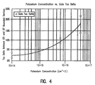
- FIG. 4 is a plot of increase in oxide (T ox ) thickness verses Potassium concentrate. Increasing the level of accumulated potassium increases the gate oxide thickness at the channel sides. Further, this increase in gate oxide thickness extends horizontally from the sides into the channel. The extent of the increased oxide thickness, both vertically and horizontally is dependent upon the level of potassium collected in the ONO layer. If the accumulated potassium level is increased sufficiently then, the gate oxide thickens across the entire device. The increase in thickness is inversely proportional to the horizontal distance from the ONO layer 124 (i.e. from the potassium catalyst).
- growth temperature and growth media affect the amount of increase in local oxide thickness derived from the presence of potassium catalyst.
- the side to center oxide thickness difference is much more pronounced, i.e., much thicker at the device sides than in the device center, for gate oxide grown at 900°C in dry O 2 than for gate oxide grown at 800°C in wet O 2 .
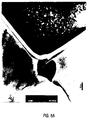
- FIG. 5 is a Transmission Electron Microscope (TEM) image of an FET corner (a cross-section at a side) grown according to the prior art at 900°C in O 2 .
- corner T ox (T ox along the side of the channel) is 8% thinner than center T ox (in the center of the channel).
- this prior art FET has a lower corner V t due to this thinner corner T ox and due to the more intense E-field from the poly both horizontally along the top channel area and vertically along the side (in the trench).
- FIG. 6A is a TEM image of an FET corner grown at 800°C in wet O 2 according to the present invention.
- corner T ox is 30% thicker center T ox .
- the V t is elevated along the channel sides over that of the prior art FET.
- the E-field is attenuated somewhat by the thicker corner T ox .
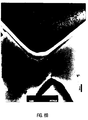
- FIG. 6B is a TEM image of a preferred embodiment FET corner grown at 900°C in dry O 2 .
- the corner T ox is 70% thicker than center T ox .
- the thickened oxide along the side of this preferred FET raises the corner V t nearly to that of the center channel V t .
- the table of FIG. 7 is a comparison of a prior art 10 ⁇ m wide FET's electrical parameters with a preferred embodiment 10 ⁇ m FET, each grown at the chip location on different wafers under nearly identical conditions. Although both devices have a nearly identical center channel v t and nearly identical on current (I ds ), the corner v t of the preferred FET is nearly equal to the center channel V t . By contrast, the corner V t of the prior art FET is 75% that of the corner V t of the preferred embodiment FET. So, for the preferred embodiment device, the retention yield at 256ms (the time that charge is held in a cell) is more than 2.6 times that of the prior art FET.
Landscapes
- Engineering & Computer Science (AREA)
- Manufacturing & Machinery (AREA)
- Semiconductor Memories (AREA)
- Metal-Oxide And Bipolar Metal-Oxide Semiconductor Integrated Circuits (AREA)
- Insulated Gate Type Field-Effect Transistor (AREA)
- Non-Volatile Memory (AREA)
Description
- The present invention relates to an integrated circuit formed on a semiconductor wafer.
- High performance and density are primary objectives of Integrated Circuit (IC) chip design. One way chip designers approach both of these objectives is by making devices and device features smaller. The smaller the device feature (and other circuit features), the tighter that circuit devices can be packed together and, consequently, the higher the circuit density. The tighter together the circuit devices are packed, the lower the wiring loads and, consequently, the faster the circuit, i.e., the higher the circuit performance. So, semiconductor process designers concentrate on reducing device features to make devices smaller and smaller.
- Just shrinking Field Effect Transistor (FET) channel length alters device characteristics such as punch through voltage and threshold voltage (Vt) to the point where the device may be unusable. So, other device parameters such as, channel doping, source/drain doping and gate oxide thickness are altered to compensate for device characteristic changes. Normally, the channel doping profile is altered to compensate for effects of the shorter channel (short channel effects). However, changes in the doping profile raise the Vt, so the doping profile change is usually accompanied with a thinner gate oxide to lower the Vt. Thinning the gate oxide intensifies the electric field from the gate on the channel. Consequently, gate capacitance per unit area is increased, gate area is decreased, and channel transconductance is increased. Overall, circuit performance improves.
- Unfortunately, as device features shrink, what had been considered superficial imperfections for older larger devices are significant flaws. Thinner gate oxide makes devices more susceptible to these flaws causing leakages and defects that reduce chip yield and impair chip reliability. Yield loss related increase in chip cost is easy to quantify because completed wafer cost must be recovered from fewer chips. Reduced reliability related cost, cost from chips failing in normal use, is a more expensive problem. These reliability failures are more expensive because they cause system down time and because of the field cost associated with finding the failing component in an assembled system containing many chips.
- FIG. 1 is a cross-sectional representation of an FET built in a 64M DRAM process. There are two
deep trenches 100 on either side of the FET 102 that isolate it from adjacent FETs. Anoxide collar 104 along thetrench 100sidewalls 106 isolates theFET 102 frompolysilicon 108 that fills the trench and is, for example, a Dynamic Random Access Memory (DRAM) cell capacitor storage plate. The gate of the FET 102 is formed by apolysilicon word line 110 that runs across a thingate oxide layer 112 the width of the FET 102. FET current flow, from drain to source (not shown), is perpendicular to the polysilicon gate and theword line 110. - A
depression 114 was formed at each side of the channel when excess oxide was removed from thecollar 104. Furthermore,collar 104 oxide formation rounded thechannel sides 116. Consequently, thechannel 102, while nearly planar in the center, is rounded at itssides 116. Thedepression 114 and rounding are flaws that were considered superficial artifacts for larger featured FETs. However, for a 64M DRAM process, they are not superficial. Poly in the depression and on therounded sides 114 enhances the E-field so that it is much more intense there than on the rest of the channel. As a result of this intensified E field, the channel sides have a lower Vt than the rest of the channel. So, the channel does not turn on at one uniform gate to source voltage (Vgs). Instead, thesides 114 turn on before and off after (i.e. with a smaller Vgs) the rest of the FET 102. - While this condition might be negligible for logic, it is unacceptable for a DRAM pass gates, because it increases pass gate channel leakage. Pass gate channel leakage allows stored charge on the storage plate to dissipate faster. This shortens DRAM retention time, i.e., the length of time that data may be stored in a DRAM cell without it needing to be reinforced or refreshed. Generally, refresh frequency is minimized because during refresh, the DRAM is unaccessible or unavailable. However, a DRAM cell with a short retention time must be refreshed more frequently than a cell with a long retention time. Consequently, a short retention time is undesirable. Thus, it is important to minimize channel leakage and so, to make FETs with planar channels for DRAMs.
- In accordance with the present invention there is now provided an integrated circuit chip as defined in claims 1 and 6.
- Viewing the present invention from another aspect, there is now provided the integrated circuit chip of Claim 1 wherein the plurality of first FETs further include an oxide collar on each side of each of said first FETs.
- An advantage of the of the present invention is that it enables selective reduction of FET channel leakage.
- Another advantage of the present invention is that it enables selective reduction of channel variations in FET threshold voltage.
- Another advantage of the present invention is that it increases DRAM cell retention time.
- Yet another advantage of the present invention is that it reduces FET feature size.
- Yet another advantage of the present invention is that it permits selective reduction of FET feature size without reducing DRAM cell retention time.
- Yet another advantage of the present invention is that it enables selective reduction in FET feature size without increasing channel leakage.
- Yet another advantage of the present invention is that it improves threshold voltage uniformity on reduced feature size FETs.
- Yet another advantage of the present invention is that it reduces channel leakage and variations in threshold voltage without impairing DRAM cell retention time for reduced feature size FETs.
- In a preferred embodiment of the present invention there is provided an integrated circuit including a plurality of first FETs with uniform gate oxide and a plurality of second FETs isolated on either side by a trench. Each second FET has a dielectric layer in the isolating trench along at least one side. The dielectric layer which may be an ONO layer has an oxidation catalyst diffused into it. The oxidation catalyst is potassium. A gate oxide along the side of the second FET in close proximity to the ONO layer is thicker than gate oxide between both sides.
- A preferred embodiment of the present invention will now be described, by way of example only, with reference to the accompanying drawings in which
- FIG. 1 is a cross-sectional representation of an FET in a DRAM made by a prior art manufacturing process:
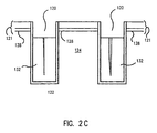
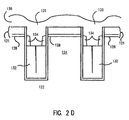
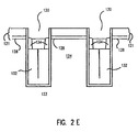
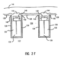
- FIGs. 2A-F represent the steps in forming an FET;
- FIGs. 3A-C represent the steps in selectively forming FETs with enhanced gate oxide and FETs with unenhanced gate oxide on the same chip according to the present invention;
- FIG. 4 is a plot of oxide thickness Tox versus Potassium concentrate;
- FIG. 5 is an image from a Transmission Electron Microscope (TEM) at a corner of an FET grown according to a prior art method;
- FIGS. 6A-B are TEM images of FETs grown according to the present invention; and
- FIG. 7 is a table comprising electrical parameters of FETs, grown according to the prior art with a preferred embodiment FET.
-
- The present invention relates to an integrated circuit as defined in claims 1 and 6.
- FIGs. 2A-F represent the steps in forming an FET which is essentially as depicted in Fig. 2F. First, in FIG. 2A,
deep trenches 120 are formed in a semiconductor layer (or wafer) 122. Prior to formingtrenches 120, a pad dielectric stack, represented bylayer stack 121, is formed on thesemiconductor layer 122. Thetrenches 120 are etched through thepad stack 121 and into thewafer 122 to isolate and define anFET region 124. A channel, source and drain will be formed in this definedFET region 124. Preferably, the semiconductor layer is silicon. In the preferred embodiment, the FET, when complete, is a passgate transistor of a Dynamic Random Access Memory (DRAM) cell. The DRAM cell's storage capacitor plate is formed in thetrench 120. - In FIG. 2B, an
ONO layer 126 is conformally formed on thepad stack 121 and intrenches 120. Although referred to as a single layer, it is understood that theONO layer 126 is a thin nitride layer sandwiched between two thin oxide layers. TheONO layer 126 lines thetrenches 120, extending vertically along the sides of eachtrench 120 past thesurface 128 of thewafer 122 and along thepad stack 121. Next, an N+ polysilicon (poly)layer 130 is deposited on theONO layer 126. - In FIG. 2C, the
polysilicon layer 130 is removed from above thepad stack 121 so thatpolysilicon 132 remains only in thetrenches 120. Preferably, thepolysilicon layer 130 is removed using Chemical-Mechanical Polish (CMP). Polishing thepolysilicon layer 130 also removes most of the ONO layer lying on thepad stack 121 such that ONO remains mainly in thetrenches 120. After CMP, residual ONO layer is removed from thepad stack 121. Then, the remainingpolysilicon 130 is etched by Reactive Ion Etching (RIE) such that the remainingpoly 132 in the trenches is recessed beneath thewafer surface 128, preferably, by 1.3µm. The preferred slurry for removing thepoly layer 130 is a poly slurry in Potassium Hydroxide, preferably < 0.1% KOH. The silicon nitride in theONO layer 126 is a diffusion barrier to the potassium in the slurry. So, potassium diffuses into theONO layer 126, through the outer oxide and collects at the nitride. Optionally, to enhance the level of collected potassium, the wafer may be dipped in a tank of KOH solution. - These steps of polishing the
poly layer 130 with a slurry containing KOH and the optional dip are contrary to conventional semiconductor chip manufacturing practices. Normally, such a use of potassium is avoided in semiconductor chip manufacture because potassium readily diffuses into silicon. Therefore, using a KOH slurry would, effectively, poison the silicon, making it unusable for forming FETs. However, theONO layer 126 blocks diffusion of the potassium and instead, collects the potassium along the interface between the outer oxide and the nitride. - Next, in FIG. 2D, an
Oxide collar 134 is selectively formed in thetrenches 120 on thepoly 132, along theONO layer 126. After forming thecollars 134, another N+ poly layer 136 is formed on thewafer 122. Thissecond poly layer 136 re-fills thetrenches 120 with polysilicon. - In FIG. 2E, the
poly layer 136 is removed from thepad stack 121 using CMP and RIE such thatpoly 140 remains only in thetrenches 120. Thepoly 140 in thetrenches 120 is coplanar with, or, slightly recessed from thewafer surface 128. As in the previous poly removal step, the preferred slurry is a poly slurry with < 0.1% KOH. A screen oxide layer (not shown) is grown in dry O2 on the exposedpad stack 121 andpoly 140, taking care to avoid removing the potassium from along the ONO layer. Then, N or P wells (if required) are defined. Next an appropriate dopant(s) is (are) ion implanted for channel tailoring. Then, the implanted dopant is diffused to the wafer as desired to bulk dope thesilicon substrate 122. - After diffusing the implanted dopants, the screen oxide layer and pad stack layers 121 are removed and gate oxide may be grown. The potassium along the
ONO layer 126 in thetrenches 120 that was collected by the nitride is a catalyst for silicon oxidation. So, as depicted in FIG. 2F, the gate oxide is thicker along thesides 142 of the channel, i.e., in close proximity to theONO layer 126. - As represented in FIGS. 3A-C, the ONO layer may be selectively removed in
non-array areas 150, prior to growing gate oxide. This results in transistors with enhanced side oxide inarrays 152 and normal transistors with unenhanced oxide innon-array areas 150. So, in FIG. 3A, all devices, both inarray areas 152 and innon-array 150, are processed as described above for the preferred embodiment transistor, through the N-well/P-well definition and bulk doping as described above with reference to FIG. 2E. - However, prior to gate oxide formation, in FIG. 3B, a
masking layer 154 is formed to defineshallow trenches 156 innon-array areas 150. After forming the shallow trench pattern in maskinglayer 154, theshallow trenches 156 are etched. The shallow trenches extend beyond thedeeper trenches 120 and, so, the ONO layer is removed from the vicinity ofchannel areas non-array area 150. - Finally, in FIG. 3C,
gate oxide 144 is formed and the poly word line and poly gates are patterned from apoly layer 146 formed on thegate oxide layer 144. An integrated circuit thus formed has FETs with essentially uniform gate oxide thickness innon-array areas 150 and with enhanced gate oxide inarray areas 152. - FIG. 4 is a plot of increase in oxide (Tox) thickness verses Potassium concentrate. Increasing the level of accumulated potassium increases the gate oxide thickness at the channel sides. Further, this increase in gate oxide thickness extends horizontally from the sides into the channel. The extent of the increased oxide thickness, both vertically and horizontally is dependent upon the level of potassium collected in the ONO layer. If the accumulated potassium level is increased sufficiently then, the gate oxide thickens across the entire device. The increase in thickness is inversely proportional to the horizontal distance from the ONO layer 124 (i.e. from the potassium catalyst).
- In addition, growth temperature and growth media affect the amount of increase in local oxide thickness derived from the presence of potassium catalyst. The side to center oxide thickness difference is much more pronounced, i.e., much thicker at the device sides than in the device center, for gate oxide grown at 900°C in dry O2 than for gate oxide grown at 800°C in wet O2.
- FIG. 5 is a Transmission Electron Microscope (TEM) image of an FET corner (a cross-section at a side) grown according to the prior art at 900°C in O2. For this prior art FET, corner Tox (Tox along the side of the channel) is 8% thinner than center Tox (in the center of the channel). Thus, this prior art FET has a lower corner Vt due to this thinner corner Tox and due to the more intense E-field from the poly both horizontally along the top channel area and vertically along the side (in the trench).
- FIG. 6A is a TEM image of an FET corner grown at 800°C in wet O2 according to the present invention. For this preferred embodiment FET, corner Tox is 30% thicker center Tox. Thus, the Vt is elevated along the channel sides over that of the prior art FET. Further, the E-field is attenuated somewhat by the thicker corner Tox.
- FIG. 6B is a TEM image of a preferred embodiment FET corner grown at 900°C in dry O2. For this preferred embodiment FET, the corner Tox is 70% thicker than center Tox. The thickened oxide along the side of this preferred FET raises the corner Vt nearly to that of the center channel Vt.
- The table of FIG. 7 is a comparison of a prior art 10µm wide FET's electrical parameters with a preferred embodiment 10µm FET, each grown at the chip location on different wafers under nearly identical conditions. Although both devices have a nearly identical center channel vt and nearly identical on current (Ids), the corner vt of the preferred FET is nearly equal to the center channel Vt. By contrast, the corner Vt of the prior art FET is 75% that of the corner Vt of the preferred embodiment FET. So, for the preferred embodiment device, the retention yield at 256ms (the time that charge is held in a cell) is more than 2.6 times that of the prior art FET.
Claims (7)
- An integrated circuit chip including a plurality of first FETs with a gate oxide of essentially uniform thickness formed in a first FET forming region (150) and a plurality of second FETs with a gate oxide of nonuniform thickness formed in a second FET forming region (152), wherein:said first FET forming region (150) comprises:first and second isolation trenches formed in said semiconductor substrate defining a first intervening FET region, said first and second isolation trenches having trench sidewalls defining first and second sides of said first intervening FET region, and a first interior FET region being centrally located between and spaced from said first and second sides of said first intervening FET region,a first gate oxide (144) located directly on said first intervening FET region, said first gate oxide extending between said first and second trenches and across said surface of said first intervening FET region, wherein said first gate oxide has essentially uniform thickness where both adjacent and meeting said first and second sides of said first intervening FET region and where said first gate oxide is located on said first interior FET region that is centrally located between and spaced from said first and second sides of said first intervening FET region; and wherein said second FET forming region (152) comprises:spaced-apart third and fourth isolation trenches (120) formed in said semiconductor substrate defining a second intervening FET region, said third and fourth isolation trenches having trench sidewalls defining first and second sides (142) of said second intervening FET region, and a second interior FET region being centrally located between and spaced from said first and second sides of said second intervening FET region,a dielectric layer (126) containing potassium as an oxidation catalyst on and along said trench sidewalls bounding said second intervening FET region,a second gate oxide (144) located directly on said second intervening FET region (152), said second gate oxide (144), extending between said third and fourth trenches and across said surface of said second intervening FET region, wherein said second gate oxide (144) has a thickness inversely proportional to the horizontal distance from the dielectric layer, whereby said second gate oxide along said sides of said second intervening FET region at said dielectric layer is thicker than second gate oxide between both said sides of said second intervening FET region.
- The integrated circuit chip of Claim 1 wherein the plurality of first FETs (152) further include an oxide collar on each side of each of said first FETs.
- The integrated circuit chip of Claim 1 wherein said dielectric layer (126) is an ONO layer.
- The integrated circuit chip of Claim 1 wherein said plurality of first FET's are isolated on either side by a trench.
- The integrated circuit chip of Claim 1 wherein the second FET forming region further includes an oxide collar on each side of each of said second FETs.
- An integrated circuit chip including a plurality of first FETs with a gate oxide of essentially uniform thickness formed in a first FET forming region (150) and a plurality of second FETs with a gate oxide of nonuniform thickness formed in a second FET forming region (152), wherein:said first FET forming region (150) comprises:first and second isolation trenches formed in said semiconductor substrate defining a first intervening FET region, said first and second isolation trenches having trench sidewalls defining first and second sides of said first intervening FET region, and a first interior FET region being centrally located between and spaced from said first and second sides of said first intervening FET region,a first gate oxide (144) located directly on said first intervening FET region, said first gate oxide (144) extending between said first and second trenches and across said surface of said first intervening FET region, wherein said first gate oxide (144) has essentially uniform thickness where both adjacent and meeting said first and second sides of said first intervening FET region and where said first gate oxide (144) is located on said first interior FET region that is centrally located between and spaced from said first and second sides of first intervening FET region ; andsaid second FET forming region (152) comprises:spaced-apart third and fourth isolation trenches (120) formed in said semiconductor substrate defining a second intervening FET region, said third and fourth isolation, trenches (120) having trench sidewalls defining first and second sides of said second intervening FET region and second interior FET region being centrally located between and spaced from said first and second sides of said second intervening FET region,an ONO layer containing potassium as an oxidation catalyst on and along said trench sidewalls bounding said second intervening FET region,a second gate oxide (144) located directly on said second intervening FET region (152), said second gate oxide extending between said third and fourth trenches (120) and across said surface of said second intervening FET region, wherein second gate oxide (144) has a thickness inversely proportional to the horizontal distance from the dielectric layer, whereby said second gate oxide along said sides of said second intervening FET region at said dielectric layer is thicker than second gate oxide between both said sides of said second intervening FET region.
- The integrated circuit chip of claim 6 wherein said plurality of first FETs are isolated on either side by a trench (120).
Applications Claiming Priority (2)
| Application Number | Priority Date | Filing Date | Title |
|---|---|---|---|
| US08/688,458 US5721448A (en) | 1996-07-30 | 1996-07-30 | Integrated circuit chip having isolation trenches composed of a dielectric layer with oxidation catalyst material |
| US688458 | 1996-07-30 |
Publications (3)
| Publication Number | Publication Date |
|---|---|
| EP0822597A2 EP0822597A2 (en) | 1998-02-04 |
| EP0822597A3 EP0822597A3 (en) | 1998-03-11 |
| EP0822597B1 true EP0822597B1 (en) | 2002-04-24 |
Family
ID=24764497
Family Applications (1)
| Application Number | Title | Priority Date | Filing Date |
|---|---|---|---|
| EP97305172A Expired - Lifetime EP0822597B1 (en) | 1996-07-30 | 1997-07-14 | Integrated circuit including field effect transisitors |
Country Status (8)
| Country | Link |
|---|---|
| US (1) | US5721448A (en) |
| EP (1) | EP0822597B1 (en) |
| JP (1) | JP3452464B2 (en) |
| KR (1) | KR100268206B1 (en) |
| CN (1) | CN1090820C (en) |
| DE (1) | DE69712138T2 (en) |
| SG (1) | SG50865A1 (en) |
| TW (1) | TW343378B (en) |
Families Citing this family (25)
| Publication number | Priority date | Publication date | Assignee | Title |
|---|---|---|---|---|
| US5933746A (en) * | 1996-04-23 | 1999-08-03 | Harris Corporation | Process of forming trench isolation device |
| US5858866A (en) * | 1996-11-22 | 1999-01-12 | International Business Machines Corportation | Geometrical control of device corner threshold |
| US7518179B2 (en) | 2004-10-08 | 2009-04-14 | Freescale Semiconductor, Inc. | Virtual ground memory array and method therefor |
| US7262997B2 (en) * | 2005-07-25 | 2007-08-28 | Freescale Semiconductor, Inc. | Process for operating an electronic device including a memory array and conductive lines |
| US7250340B2 (en) * | 2005-07-25 | 2007-07-31 | Freescale Semiconductor, Inc. | Method of fabricating programmable structure including discontinuous storage elements and spacer control gates in a trench |
| US7211487B2 (en) * | 2005-07-25 | 2007-05-01 | Freescale Semiconductor, Inc. | Process for forming an electronic device including discontinuous storage elements |
| US7642594B2 (en) * | 2005-07-25 | 2010-01-05 | Freescale Semiconductor, Inc | Electronic device including gate lines, bit lines, or a combination thereof |
| US7285819B2 (en) * | 2005-07-25 | 2007-10-23 | Freescale Semiconductor, Inc. | Nonvolatile storage array with continuous control gate employing hot carrier injection programming |
| US7619270B2 (en) * | 2005-07-25 | 2009-11-17 | Freescale Semiconductor, Inc. | Electronic device including discontinuous storage elements |
| US7226840B2 (en) * | 2005-07-25 | 2007-06-05 | Freescale Semiconductor, Inc. | Process for forming an electronic device including discontinuous storage elements |
| US20070020840A1 (en) * | 2005-07-25 | 2007-01-25 | Freescale Semiconductor, Inc. | Programmable structure including nanocrystal storage elements in a trench |
| US7256454B2 (en) * | 2005-07-25 | 2007-08-14 | Freescale Semiconductor, Inc | Electronic device including discontinuous storage elements and a process for forming the same |
| US7314798B2 (en) * | 2005-07-25 | 2008-01-01 | Freescale Semiconductor, Inc. | Method of fabricating a nonvolatile storage array with continuous control gate employing hot carrier injection programming |
| US7582929B2 (en) * | 2005-07-25 | 2009-09-01 | Freescale Semiconductor, Inc | Electronic device including discontinuous storage elements |
| US7205608B2 (en) * | 2005-07-25 | 2007-04-17 | Freescale Semiconductor, Inc. | Electronic device including discontinuous storage elements |
| US7112490B1 (en) * | 2005-07-25 | 2006-09-26 | Freescale Semiconductor, Inc. | Hot carrier injection programmable structure including discontinuous storage elements and spacer control gates in a trench |
| US7619275B2 (en) * | 2005-07-25 | 2009-11-17 | Freescale Semiconductor, Inc. | Process for forming an electronic device including discontinuous storage elements |
| US7394686B2 (en) * | 2005-07-25 | 2008-07-01 | Freescale Semiconductor, Inc. | Programmable structure including discontinuous storage elements and spacer control gates in a trench |
| US7592224B2 (en) | 2006-03-30 | 2009-09-22 | Freescale Semiconductor, Inc | Method of fabricating a storage device including decontinuous storage elements within and between trenches |
| US7759731B2 (en) * | 2006-08-28 | 2010-07-20 | Advanced Analogic Technologies, Inc. | Lateral trench MOSFET with direct trench polysilicon contact and method of forming the same |
| US7651916B2 (en) * | 2007-01-24 | 2010-01-26 | Freescale Semiconductor, Inc | Electronic device including trenches and discontinuous storage elements and processes of forming and using the same |
| US7838922B2 (en) * | 2007-01-24 | 2010-11-23 | Freescale Semiconductor, Inc. | Electronic device including trenches and discontinuous storage elements |
| US7572699B2 (en) * | 2007-01-24 | 2009-08-11 | Freescale Semiconductor, Inc | Process of forming an electronic device including fins and discontinuous storage elements |
| CN101170074B (en) * | 2007-11-13 | 2010-08-11 | 北京大学 | A Method of Improving the Anti-irradiation Characteristics of Ultra-deep Submicron MOSFET |
| EP3637457B1 (en) * | 2018-10-09 | 2026-04-22 | Infineon Technologies Austria AG | Transistor device and method for forming a recess for a trench gate electrode |
Family Cites Families (30)
| Publication number | Priority date | Publication date | Assignee | Title |
|---|---|---|---|---|
| JPS6043024B2 (en) * | 1978-12-30 | 1985-09-26 | 富士通株式会社 | Manufacturing method of semiconductor device |
| US4356211A (en) * | 1980-12-19 | 1982-10-26 | International Business Machines Corporation | Forming air-dielectric isolation regions in a monocrystalline silicon substrate by differential oxidation of polysilicon |
| IT1211079B (en) * | 1981-07-20 | 1989-09-29 | Sibit S P A Ora Tioxide Italia | CATALYSTS FOR PHOTO-ASSISTED OXIDE-REDUCTION REACTIONS. |
| JPS58202545A (en) * | 1982-05-21 | 1983-11-25 | Toshiba Corp | Manufacture of semiconductor device |
| DD242905A1 (en) * | 1985-11-20 | 1987-02-11 | Halbleiterwerk Veb | PROCESS FOR PREPARING THERMAL SIO DEEP 2-ISOLATOR LAYERS |
| JPS632371A (en) * | 1986-06-23 | 1988-01-07 | Hitachi Ltd | semiconductor equipment |
| JPH0793374B2 (en) * | 1986-12-18 | 1995-10-09 | 沖電気工業株式会社 | CMIS type dynamic memory device |
| JPS63240043A (en) * | 1987-03-27 | 1988-10-05 | Matsushita Electric Ind Co Ltd | Manufacture of semiconductor device |
| JPS6427252A (en) * | 1987-04-13 | 1989-01-30 | Nec Corp | Semiconductor storage device |
| JPS63299262A (en) * | 1987-05-29 | 1988-12-06 | Nec Corp | Semiconductor device |
| EP0333426B1 (en) * | 1988-03-15 | 1996-07-10 | Kabushiki Kaisha Toshiba | Dynamic RAM |
| US4986878A (en) * | 1988-07-19 | 1991-01-22 | Cypress Semiconductor Corp. | Process for improved planarization of the passivation layers for semiconductor devices |
| KR910007181B1 (en) * | 1988-09-22 | 1991-09-19 | 현대전자산업 주식회사 | Side-wall doped trench and stacked capacitor cell and method manufacturing thereof |
| TW199237B (en) * | 1990-07-03 | 1993-02-01 | Siemens Ag | |
| US5078801A (en) * | 1990-08-14 | 1992-01-07 | Intel Corporation | Post-polish cleaning of oxidized substrates by reverse colloidation |
| JPH05152429A (en) * | 1991-11-28 | 1993-06-18 | Nec Corp | Method for manufacturing semiconductor device |
| US5358894A (en) * | 1992-02-06 | 1994-10-25 | Micron Technology, Inc. | Oxidation enhancement in narrow masked field regions of a semiconductor wafer |
| US5217919A (en) * | 1992-03-19 | 1993-06-08 | Harris Corporation | Method of forming island with polysilicon-filled trench isolation |
| US5292679A (en) * | 1992-04-23 | 1994-03-08 | Nippon Steel Corporation | Process for producing a semiconductor memory device having memory cells including transistors and capacitors |
| US5240875A (en) * | 1992-08-12 | 1993-08-31 | North American Philips Corporation | Selective oxidation of silicon trench sidewall |
| US5313419A (en) * | 1993-02-01 | 1994-05-17 | National Semiconductor Corporation | Self-aligned trench isolation scheme for select transistors in an alternate metal virtual ground (AMG) EPROM array |
| US5422294A (en) * | 1993-05-03 | 1995-06-06 | Noble, Jr.; Wendell P. | Method of making a trench capacitor field shield with sidewall contact |
| US5316965A (en) * | 1993-07-29 | 1994-05-31 | Digital Equipment Corporation | Method of decreasing the field oxide etch rate in isolation technology |
| US5397725A (en) * | 1993-10-28 | 1995-03-14 | National Semiconductor Corporation | Method of controlling oxide thinning in an EPROM or flash memory array |
| JP3159850B2 (en) * | 1993-11-08 | 2001-04-23 | シャープ株式会社 | Nonvolatile semiconductor memory device and method of manufacturing the same |
| US5406515A (en) * | 1993-12-01 | 1995-04-11 | International Business Machines Corporation | Method for fabricating low leakage substrate plate trench DRAM cells and devices formed thereby |
| US5536675A (en) * | 1993-12-30 | 1996-07-16 | Intel Corporation | Isolation structure formation for semiconductor circuit fabrication |
| JP3383404B2 (en) * | 1994-03-16 | 2003-03-04 | 株式会社東芝 | Method for manufacturing semiconductor device |
| US5448090A (en) * | 1994-08-03 | 1995-09-05 | International Business Machines Corporation | Structure for reducing parasitic leakage in a memory array with merged isolation and node trench construction |
| US5426324A (en) * | 1994-08-11 | 1995-06-20 | International Business Machines Corporation | High capacitance multi-level storage node for high density TFT load SRAMs with low soft error rates |
-
1996
- 1996-07-30 US US08/688,458 patent/US5721448A/en not_active Expired - Fee Related
-
1997
- 1997-05-28 KR KR1019970021148A patent/KR100268206B1/en not_active Expired - Fee Related
- 1997-06-27 CN CN97113530A patent/CN1090820C/en not_active Expired - Fee Related
- 1997-07-09 SG SG1997002418A patent/SG50865A1/en unknown
- 1997-07-14 DE DE69712138T patent/DE69712138T2/en not_active Expired - Fee Related
- 1997-07-14 EP EP97305172A patent/EP0822597B1/en not_active Expired - Lifetime
- 1997-07-28 JP JP21707897A patent/JP3452464B2/en not_active Expired - Fee Related
- 1997-07-30 TW TW086110887A patent/TW343378B/en not_active IP Right Cessation
Also Published As
| Publication number | Publication date |
|---|---|
| JP3452464B2 (en) | 2003-09-29 |
| KR100268206B1 (en) | 2000-10-16 |
| SG50865A1 (en) | 1998-07-20 |
| US5721448A (en) | 1998-02-24 |
| TW343378B (en) | 1998-10-21 |
| JPH1074912A (en) | 1998-03-17 |
| DE69712138D1 (en) | 2002-05-29 |
| KR980012616A (en) | 1998-04-30 |
| EP0822597A2 (en) | 1998-02-04 |
| CN1090820C (en) | 2002-09-11 |
| CN1175092A (en) | 1998-03-04 |
| DE69712138T2 (en) | 2003-01-30 |
| EP0822597A3 (en) | 1998-03-11 |
Similar Documents
| Publication | Publication Date | Title |
|---|---|---|
| US5824580A (en) | Method of manufacturing an insulated gate field effect transistor | |
| US5721448A (en) | Integrated circuit chip having isolation trenches composed of a dielectric layer with oxidation catalyst material | |
| KR100560647B1 (en) | Reduced parasitic leakage in semiconductor devices | |
| US6204140B1 (en) | Dynamic random access memory | |
| EP1199745A2 (en) | Vertical transistor trench capacitor DRAM with SOI logic devices | |
| US6258659B1 (en) | Embedded vertical DRAM cells and dual workfunction logic gates | |
| US20060273406A1 (en) | Semiconductor integrated circuit device having deposited layer for gate insulation | |
| CN1262527A (en) | Dynamic RAM | |
| US7190042B2 (en) | Self-aligned STI for narrow trenches | |
| KR20030020290A (en) | Self-limiting polysilicon buffered locos for dram cell | |
| US6812091B1 (en) | Trench capacitor memory cell | |
| EP0822591B1 (en) | Insulated gate field effect transistor | |
| US7510930B2 (en) | Method for fabricating recessed gate MOS transistor device | |
| US5332682A (en) | Local encroachment reduction | |
| US6294424B1 (en) | Method for fabricating a semiconductor device | |
| US5109259A (en) | Multiple DRAM cells in a trench | |
| US7700435B2 (en) | Method for fabricating deep trench DRAM array | |
| KR900005355B1 (en) | Semiconductor memory device and manufacturing method thereof | |
| KR100238194B1 (en) | Capacitor of Semiconductor Memory Device and Manufacturing Method Thereof | |
| US20050158947A1 (en) | Method for Forming Self-Aligned Trench | |
| JPH08222708A (en) | Semiconductor memory device and manufacturing method thereof | |
| HK1029661A (en) | Dynamic random access memory | |
| WO1990005377A1 (en) | Local encroachment reduction |
Legal Events
| Date | Code | Title | Description |
|---|---|---|---|
| PUAI | Public reference made under article 153(3) epc to a published international application that has entered the european phase |
Free format text: ORIGINAL CODE: 0009012 |
|
| PUAL | Search report despatched |
Free format text: ORIGINAL CODE: 0009013 |
|
| AK | Designated contracting states |
Kind code of ref document: A2 Designated state(s): DE FR GB IT |
|
| AX | Request for extension of the european patent |
Free format text: AL;LT;LV;RO;SI |
|
| AK | Designated contracting states |
Kind code of ref document: A3 Designated state(s): AT BE CH DE DK ES FI FR GB GR IE IT LI LU MC NL PT SE |
|
| AX | Request for extension of the european patent |
Free format text: AL;LT;LV;RO;SI |
|
| 17P | Request for examination filed |
Effective date: 19980902 |
|
| AKX | Designation fees paid |
Free format text: DE FR GB IT |
|
| RBV | Designated contracting states (corrected) |
Designated state(s): DE FR GB IT |
|
| 17Q | First examination report despatched |
Effective date: 19991011 |
|
| GRAG | Despatch of communication of intention to grant |
Free format text: ORIGINAL CODE: EPIDOS AGRA |
|
| GRAG | Despatch of communication of intention to grant |
Free format text: ORIGINAL CODE: EPIDOS AGRA |
|
| GRAH | Despatch of communication of intention to grant a patent |
Free format text: ORIGINAL CODE: EPIDOS IGRA |
|
| GRAH | Despatch of communication of intention to grant a patent |
Free format text: ORIGINAL CODE: EPIDOS IGRA |
|
| REG | Reference to a national code |
Ref country code: GB Ref legal event code: IF02 |
|
| GRAA | (expected) grant |
Free format text: ORIGINAL CODE: 0009210 |
|
| AK | Designated contracting states |
Kind code of ref document: B1 Designated state(s): DE FR GB IT |
|
| REG | Reference to a national code |
Ref country code: GB Ref legal event code: FG4D |
|
| REF | Corresponds to: |
Ref document number: 69712138 Country of ref document: DE Date of ref document: 20020529 |
|
| PGFP | Annual fee paid to national office [announced via postgrant information from national office to epo] |
Ref country code: GB Payment date: 20020701 Year of fee payment: 6 |
|
| PGFP | Annual fee paid to national office [announced via postgrant information from national office to epo] |
Ref country code: FR Payment date: 20020715 Year of fee payment: 6 |
|
| ET | Fr: translation filed | ||
| PLBE | No opposition filed within time limit |
Free format text: ORIGINAL CODE: 0009261 |
|
| STAA | Information on the status of an ep patent application or granted ep patent |
Free format text: STATUS: NO OPPOSITION FILED WITHIN TIME LIMIT |
|
| 26N | No opposition filed |
Effective date: 20030127 |
|
| PG25 | Lapsed in a contracting state [announced via postgrant information from national office to epo] |
Ref country code: GB Free format text: LAPSE BECAUSE OF NON-PAYMENT OF DUE FEES Effective date: 20030714 |
|
| GBPC | Gb: european patent ceased through non-payment of renewal fee |
Effective date: 20030714 |
|
| PG25 | Lapsed in a contracting state [announced via postgrant information from national office to epo] |
Ref country code: FR Free format text: LAPSE BECAUSE OF NON-PAYMENT OF DUE FEES Effective date: 20040331 |
|
| REG | Reference to a national code |
Ref country code: FR Ref legal event code: ST |
|
| PGFP | Annual fee paid to national office [announced via postgrant information from national office to epo] |
Ref country code: DE Payment date: 20090929 Year of fee payment: 13 |
|
| PGFP | Annual fee paid to national office [announced via postgrant information from national office to epo] |
Ref country code: IT Payment date: 20090716 Year of fee payment: 13 |
|
| PG25 | Lapsed in a contracting state [announced via postgrant information from national office to epo] |
Ref country code: DE Free format text: LAPSE BECAUSE OF NON-PAYMENT OF DUE FEES Effective date: 20110201 |
|
| REG | Reference to a national code |
Ref country code: DE Ref legal event code: R119 Ref document number: 69712138 Country of ref document: DE Effective date: 20110201 |
|
| PG25 | Lapsed in a contracting state [announced via postgrant information from national office to epo] |
Ref country code: IT Free format text: LAPSE BECAUSE OF NON-PAYMENT OF DUE FEES Effective date: 20100714 |