EP0820171B1 - Emeteur ou récepteur pour porteurs multiples avec rotateurs de phase - Google Patents
Emeteur ou récepteur pour porteurs multiples avec rotateurs de phase Download PDFInfo
- Publication number
- EP0820171B1 EP0820171B1 EP96202004A EP96202004A EP0820171B1 EP 0820171 B1 EP0820171 B1 EP 0820171B1 EP 96202004 A EP96202004 A EP 96202004A EP 96202004 A EP96202004 A EP 96202004A EP 0820171 B1 EP0820171 B1 EP 0820171B1
- Authority
- EP
- European Patent Office
- Prior art keywords
- transmit
- data symbols
- transmit data
- digital
- analogue
- Prior art date
- Legal status (The legal status is an assumption and is not a legal conclusion. Google has not performed a legal analysis and makes no representation as to the accuracy of the status listed.)
- Expired - Lifetime
Links
Images

Classifications
-
- H—ELECTRICITY
- H04—ELECTRIC COMMUNICATION TECHNIQUE
- H04L—TRANSMISSION OF DIGITAL INFORMATION, e.g. TELEGRAPHIC COMMUNICATION
- H04L27/00—Modulated-carrier systems
- H04L27/26—Systems using multi-frequency codes
- H04L27/2601—Multicarrier modulation systems
- H04L27/2647—Arrangements specific to the receiver only
- H04L27/2655—Synchronisation arrangements
- H04L27/2668—Details of algorithms
- H04L27/2673—Details of algorithms characterised by synchronisation parameters
- H04L27/2675—Pilot or known symbols
-
- H—ELECTRICITY
- H04—ELECTRIC COMMUNICATION TECHNIQUE
- H04B—TRANSMISSION
- H04B3/00—Line transmission systems
- H04B3/02—Details
- H04B3/20—Reducing echo effects or singing; Opening or closing transmitting path; Conditioning for transmission in one direction or the other
- H04B3/21—Reducing echo effects or singing; Opening or closing transmitting path; Conditioning for transmission in one direction or the other using a set of bandfilters
-
- H—ELECTRICITY
- H04—ELECTRIC COMMUNICATION TECHNIQUE
- H04L—TRANSMISSION OF DIGITAL INFORMATION, e.g. TELEGRAPHIC COMMUNICATION
- H04L27/00—Modulated-carrier systems
- H04L27/26—Systems using multi-frequency codes
- H04L27/2601—Multicarrier modulation systems
- H04L27/2626—Arrangements specific to the transmitter only
-
- H—ELECTRICITY
- H04—ELECTRIC COMMUNICATION TECHNIQUE
- H04L—TRANSMISSION OF DIGITAL INFORMATION, e.g. TELEGRAPHIC COMMUNICATION
- H04L27/00—Modulated-carrier systems
- H04L27/26—Systems using multi-frequency codes
- H04L27/2601—Multicarrier modulation systems
- H04L27/2647—Arrangements specific to the receiver only
- H04L27/2655—Synchronisation arrangements
- H04L27/2657—Carrier synchronisation
-
- H—ELECTRICITY
- H04—ELECTRIC COMMUNICATION TECHNIQUE
- H04L—TRANSMISSION OF DIGITAL INFORMATION, e.g. TELEGRAPHIC COMMUNICATION
- H04L7/00—Arrangements for synchronising receiver with transmitter
- H04L7/04—Speed or phase control by synchronisation signals
- H04L7/041—Speed or phase control by synchronisation signals using special codes as synchronising signal
- H04L2007/045—Fill bit or bits, idle words
-
- H—ELECTRICITY
- H04—ELECTRIC COMMUNICATION TECHNIQUE
- H04L—TRANSMISSION OF DIGITAL INFORMATION, e.g. TELEGRAPHIC COMMUNICATION
- H04L7/00—Arrangements for synchronising receiver with transmitter
- H04L7/0091—Transmitter details
Definitions
- the present invention relates to DMT transmission.
- Such a transmission is already known in the art, e.g. from the contribution to the ADSL Standard T1E1.4 with reference number T1E1.4 / 93-025, written by John M. Cioffi and Po T . Tong , and entitled 'VLSI DMT Implementation for ADSL '.
- the DMT modem comprises a transmitting part and a receiving part, combined in what is called a central office ADSL transceiver on page 1, and a remote terminal ADSL transceiver on page 2.
- these transceivers include a digital signal processor.
- This digital signal processor (see page 5, paragraph 2.2 and Fig. 4, or see page 12 paragraph 3.2 and Fig. 7) comprises modulation means, named a complex-to-real IFFT (Inverse Fast Fourier Transformer), and demodulation means, named a real-to-complex FFT (Fast Fourier Transformer).
- modulation means named a complex-to-real IFFT (Inverse Fast Fourier Transformer)
- demodulation means named a real-to-complex FFT (Fast Fourier Transformer).
- the modulation means IFFT are coupled to a digital to analogue converter DAC
- the demodulation means FFT are preceded by an analogue to digital converter, not shown in Fig. 4 but for evident reasons present.
- the analogue to digital converter in the receiving part and the digital to analogue converter in the transmitting part may operate under control of one clock or different clocks which are synchronised.
- DMT symbols echoes of transmit data symbols
- the transceiver in Fig. 4 further is provided with an echo canceller. If transmit data symbols and received data symbols are not aligned when entering the echo canceller, echo cancellation becomes rather complex since echoes of more than one transmit data symbol should then be cancelled within a received data symbol.
- An object of the present invention is to provide a transmitter and a method of the above known type, but wherein transmit data symbols and received data symbols are aligned, and consequently wherein the complexity of echo cancellation is reduced.
- phase rotation applied to the transmit data symbols will increase or decrease gradually in time for successive transmit data symbols since the misalignment between transmit data symbols and received data symbols changes gradually in time due to a clock speed difference between the clocks of two communicating modems.
- the vectors representing the carriers of transmit data symbols are rotating when the vectors representing the carriers of received data symbols are fixed, and vice versa.
- This rotation is compensated for by the transmit rotation means.
- the skip/stuff means is activated to duplicate or to delete one sample in a transmit data symbol so that the rotation to be applied by the transmit rotation means again decreases by an equivalent amount.
- the present invention is not only dedicated to be used in echo cancelling environments but also is very suitable for systems wherein upstream and downstream transmission takes place in separate time intervals.
- TDD time division duplexing
- alignment of upstream and downstream travelling symbols is recommended, as will be recognised by a person skilled in the art.
- TDM time division multiplexing
- transmitter/receiver alignment for echo canceller complexity reduction is also already known from the publication " Frequency Domain Echo Cancellation for Discrete Multitone Asymmetric Digital Subscriber Line Transceivers" from the author David C. Jones.
- This publication in IEEE Transactions on Communications, Vol. 43, No. 2/4, February 1995, pages 1663-1672 teaches to compensate for the number of samples by which transmit symbols lead the received symbols through sample skip/stuff means integrated in the parallel to serial converter. The accuracy that is obtainable through this technique is 1/2 sample. Thus, this technique is not adequate to compensate for clock speed differences between the transmitter and receiver. Thereto, a phase rotor is needed and sample skip/stuff means that duplicate or delete samples in proper relation with the rotation of the carriers.
- an optional feature of the transmitter according to the present invention is that it further may be equipped with activation means as defined in claim 2.
- modulator/demodulator may also include receive rotation means and receive skip/stuff means.
- a feature of the present modulator/demodulator is that it also may be equipped with activation means as defined by claim 2.
- modulator/demodulator may further include communication means and decision means
- a communication between two connected modems can be set up at initialisation of the system to decide in which modem the rotating means and the skip/stuff means will be activated.
- Different decision criteria can be used by the decision means.
- a first possible strategy might be based on the rule that the central office modem always acts as the master of the remote terminal modem. Thus, the remote terminal will have to activate its rotating and skip/stuff means to adapt its received data symbols and transmit data symbols in accordance to the central office clock.
- a second strategy might be that the central office modem slaves to the remote terminal modem and therefore activates its rotation means and skip/stuff means.
- a characteristic feature of the present modulator/demodulator is that it may be equipped with phase difference measurement means.
- the measured phase difference between the received pilot tone and expected received pilot tone serves as a measure for the phase rotation that has to be applied to the transmit data carriers.
- this phase difference variation is a measure for the clock speed difference between the clocks of the two communicating modems. It is however evident that any other estimate of the clock speed difference and means executing this estimate may replace the phase difference measurement means.
- phase difference measurement means may also control the receive rotation means and skip/stuff means.
- phase rotation applied to the received data symbols can also be made proportional to the measured phase difference.
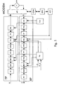
- the modulator/demodulator MODEM in Fig. 1 includes a transmitting part TP and a receiving part RP.
- the transmitting part TP comprises a serial to parallel converter SP, a mapper MAP, a transmit rotation means TROT, an inverse fast fourier transformer IFFT, a cyclic prefix extender CPEX, a transmit skip/stuff means TSS, a parallel to serial converter PS and a digital to analogue converter DA.
- the receiving part RP comprises an analogue to digital converter AD, a time domain equaliser TEQ, a serial to parallel converter SP', a receive skip/stuff means RSS, a cyclic prefix eraser CPER, a fast fourier transformer FFT, a frequency domain equaliser FEQ, a receive rotation means RROT, a demapper DMAP, and a parallel to serial converter PS'. It is noticed that the order of the receive rotation means RROT and frequency domain equaliser FEQ might be reversed, and the time domain equaliser TEQ might be missing.
- the modulator/demodulator MODEM further is provided with an analogue front end AFE, a hybrid means H, a communication means COM, a decision means DEC, an activation means ACT, a phase locked loop PLL and a clock CLK.
- the serial to parallel converter SP In the transmitting part TP, the serial to parallel converter SP, the mapper MAP, the transmit rotation means TROT, the inverse fast fourier transformer IFFT, the cyclic prefix extender CPEX, the transmit skip/stuff means TSS, the parallel to serial converter PS and the digital to analogue converter DA are cascade connected between a digital data input D and an analogue signal output S.
- the analogue signal output S is coupled to a transmission line L via the analogue front end AFE and hybrid means H. Via this hybrid means H and the analogue front end AFE, the transmission line L is also coupled to an analogue signal input S' of the receiving part RP.
- the analogue to digital converter AD Inside the receiving part RP, the analogue to digital converter AD, the time domain equaliser TEQ, the serial to parallel converter SP', the receive skip/stuff means RSS, the cyclic prefix eraser CPER, the fast fourier transformer FFT, the frequency domain equaliser FEQ, the receive rotation means RROT, the demapper DMAP and the parallel to serial converter PS' are series connected between the analogue signal input S' and a digital data output D'.
- An output of the receive rotation means RROT is also coupled to a pilot tone input PT of the phase locked loop PLL, a second input of which, called an expected pilot tone input PT_E, is coupled to an expected pilot tone generator not shown in Fig. 1.
- Output links of the phase locked loop PLL are connected to control inputs of the transmit rotation means TROT, the transmit skip/stuff means TSS, the receive rotation means RROT and the receive skip/stuff means RSS respectively.
- the communication means COM is coupled to the analogue front end AFE.
- this bi-directional link is represented by a single line directly interconnecting the communication means COM and the analogue front end AFE.
- an output of the communication means COM serves as an additional input for the transmitting part TP and an input of the communication means COM is connected to an additional output of the receiving part RP.
- the communication means COM is not directly connected to the analogue front end AFE but communicates with this analogue front end AFE via the receiving part RP and transmitting part TP of the modem MODEM.
- a terminal of the communication means COM and a terminal of the decision means DEC are bidirectionally interconnected, and an output of the decision means DEC is coupled to an input of the activation means ACT.
- the activation means ACT has a plurality of outgoing connections, to the transmit rotation means TROT and transmit skip/stuff means TSS, to the receive rotation means RROT and receive skip/stuff means RSS respectively.
- An output of the clock CLK is connected to clock inputs of both the digital to analogue converter DA and analogue to digital converter AD.
- the clock CLK in Fig. 1 is supposed to be a fixed clock or a voltage controlled oscillator for coarse tuning of the clock period.
- the communication system drawn therein includes a first modulator/demodulator MODEM1 which forms part of a central office CO, and a second modulator/demodulator MODEM2 which forms part of a remote terminal RT. Both modems, MODEM1 and MODEM2, are coupled via a transmission line TL.
- the transmit rotation means TROT, transmit skip/stuff means TSS, receive rotation means RROT and receive skip/stuff means RSS in the modem MODEM2 of the remote terminal RT will be activated and the functionality of these blocks will be described.
- the transmission line TL in Fig. 2 represents a twisted pair telephone line.
- Asymmetric Digital Subscriber Line ADSL
- Discrete Multi Tone (DMT) modulation is used to modulate digital information on a set of carriers with equidistant frequencies.
- DMT Discrete Multi Tone
- ADSL Advanced Digital Subscriber Line
- ANSI American National Standards Institute, Inc.
- the upstream and downstream channels may be separated by frequency division multiplexing (FDM) or by echo cancelling.
- FDM frequency division multiplexing
- the approved version of the above ANSI Standard on ADSL is referred to as ANSI T1.413 and is entitled 'Network and Customer Installation Interfaces, Asymmetric Digital Subscriber Line (ADSL) Metallic Interface'.
- time division duplexing (TDD) could be used.
- TDD Time Division duplexing
- some or all carriers may be used for modulation of data thereon in the upstream direction as well as in the downstream direction.
- the present invention is more useful in echo cancelling and TDD (Time Division Duplexing) environments although its application is not excluded in FDM (Frequency Division Multiplexing) systems.
- the modulator/demodulator MODEM is supposed to be equipped with an echo canceller between its transmitting part TP and receiving part RP.
- this modem MODEM2 is of the type of MODEM in Fig. 1 wherein the activation means ACT de-activates the transmit rotation means TROT, the transmit skip/stuff means TSS, the receive rotation means RROT, and the receive skip/stuff means RSS.
- the activation means ACT de-activates the transmit rotation means TROT, the transmit skip/stuff means TSS, the receive rotation means RROT, and the receive skip/stuff means RSS.
- MODEM2 modulates digital data D on a set of carriers, each one being modulated by QAM (Quadrature Amplitude Modulation) modulation.
- QAM Quadrature Amplitude Modulation
- the digital data stream D which is a serial sequence of bits, thereto is parallelised by the serial to parallel converter SP.
- the mapper MAP then allocates to each one of the carriers a dedicated amount of bits to be modulated thereon. These different amounts are calculated taking into account parameters such as the signal to noise ratio and the line attenuation on each carrier. Obviously, a carrier which is less attenuated by the line is allowed to carry more bits than a high attenuated or disturbed carrier. As a result, three bits will for instance be modulated by 8 QAM modulation on the first carrier, 9 bits will for instance be modulated by 512 QAM modulation on the second carrier, and so on, thereby generating frequency domain DMT symbols.
- these DMT symbols are transformed from frequency domain to time domain.
- the cyclic prefix extender CPEX then extends each DMT symbol with a fixed length prefix to preventively protect transmit DMT symbols against intersymbol and intercarrier interference due to transmission over the telephone line TL.
- Successive DMT symbols are then serialised by the parallel to serial converter PS and converted into an analogue signal S by the digital to analogue converter DA.
- an analogue signal S' arriving at MODEM2 is demodulated by the receiving part RP thereof and converted into a digital output signal D'.
- the analogue signal S' is digitised in the analogue to digital converter AD.
- the time domain equaliser filters the received samples with a digital filter that is constituted to shorten the length of the transmission line impulse response. Successive samples in the digitised stream that belong to the same DMT symbol are parallelised by the serial to parallel converter SP'.
- the cyclic prefix is erased from the DMT symbols in the cyclic prefix eraser CPER, and the fast fourier transform processor FFT transforms the time domain DMT symbols into frequency domain DMT symbols.
- the demapper DMAP is aware of the bit constellations of the different carriers and QAM demodulates the different carriers to obtain the exact number of bits therefrom. Via the parallel to serial converter PS', the demodulated bits are then serialised and applied to the digital data output D' of the receiving part RP.
- the analogue front end AFE and hybrid means H convert and condition the signals, S and S', to and from the transmission line. Front-end filtering and transmission line coupling for instance are performed with the appropriate levels of linearity and noise. Plain analogue telephone signals transmitted in the lower frequency bands, are separated from the digital data by a splitter provided thereto.
- MODEM1 in the central office CO a similar structure can be described. The working thereof in up- and downstream direction is completely equivalent to that of the DMT modem MODEM2 in the remote terminal RT. Only the clock that is used in the central office CO to control the digital to analogue converter DA and analogue to digital converter AD is different from that used in the remote terminal RT. It is assumed that, in each one of the modems, MODEM1 and MODEM2, the same clock is used for the analogue to digital converter and the digital to analogue converter. Alternatively, in each modem, the analogue to digital converter clock could be derived from the digital to analogue converter clock or vice versa. As a result, upstream and downstream travelling DMT symbols are sampled differently.
- upstream travelling DMT symbols are sampled under control of the remote terminal clock, whilst downstream travelling DMT symbols are sampled under control of the central office clock.
- downstream travelling DMT symbols are sampled under control of the remote terminal clock which is slower or faster than the central office clock.
- the received DMT symbols are sampled too fast or too slow. This would cause a loss of DMT symbol alignment and a rotation of the received QAM modulated symbols. Therefore, in the following paragraph, it is supposed that the activation means ACT in the remote terminal RT activates the receive rotation means RROT and the receive skip/stuff means RSS.
- the sample clock speed difference is compensated for by the receive rotation means RROT and the receive skip/stuff means RSS in the modem MODEM2 of the remote terminal when it is supposed that these means are activated.
- one of the carriers of DMT symbols is reserved as pilot tone.
- This pilot tone is observed in the received DMT symbols at the output of the receive rotation means RROT and is applied to the pilot tone input PT of the phase locked loop PLL.
- the phase locked loop PLL measures the phase difference between this pilot tone PT and a pilot tone that was expected to be received PT_E.
- the resulting phase difference variation is a measure for the clock speed difference between the clocks of the modem MODEM1 in the central office CO and the modem MODEM2 in the remote terminal RT.
- each carrier thereof has to be rotated over a phase that is proportional to the measured phase difference, and proportional to its own frequency.
- carrier 1 has to be phase rotated over a phase ⁇
- carrier 2 having a double frequency of carrier 1
- the factor ⁇ depends on the measured phase difference between the pilot tone PT and expected pilot tone PT_E, and will increase gradually since this phase difference grows stepwise for each successively received DMT symbol.
- the magnitude of the step depends on the already mentioned difference in clock speeds.
- the receive rotation means RROT under control of the phase locked loop PLL is able to compensate for the clock speed differences between central office CO and remote terminal RT.
- the receive skip/stuff means RSS is activated to duplicate or to delete one sample in the received DMT symbol, so that the phase rotation that has to be applied to the different carriers by RROT again reduces.
- the transmitted symbols have to be processed before applying them to the transmission line TL. Since this alignment implies a shift in time, forward or backward, and a rotation in phase which is proportional to the clock speed difference between remote terminal RT and central office CO and in proportion to the frequency of the respective carrier, the processing can again be performed by a rotation means and skip/stuff means.
- the transmit rotation means TROT and transmit skip/stuff means TSS are included thereto.
- the transmit rotation means TROT and transmit skip/stuff means TSS of the remote terminal RT When activated by the activation means ACT, the transmit rotation means TROT and transmit skip/stuff means TSS of the remote terminal RT will apply phase rotations to the different carriers whereon the transmit data D are modulated so that the transmit DMT symbols in S are virtually aligned with the received DMT symbols in S' at the transmission line TL. Samples of the transmitted DMT symbols are duplicated or deleted by the transmit skip/stuff means TSS whenever the time shift to be applied to transmit DMT symbols reaches half a sample period of the central office clock.
- the central office modem MODEM1 sends for instance a pilot tone to the remote terminal modem MODEM2.
- This modem MODEM2 locks on this pilot by adjusting its receive clock.
- it adjusts its transmit clock in accordance to the measured clock difference between MODEM1 and MODEM2.
- each modem measures the transmission line and calculates an optimal DMT symbol alignment.
- each modem can transmit known data sequences.
- Each modem then adjusts its symbol alignment in accordance to the measured value.
- both modems, MODEM1 in the central office CO and the modem MODEM2 in the remote terminal RT are equipped with a transmit rotation means TROT, transmit skip/stuff means TSS, receive rotation means RROT, and receive skip/stuff means RSS.
- these means, RROT, TROT, RSS and TSS have to be activated in only one of the two modems, MODEM1 and MODEM2.
- the modems MODEM1 and MODEM2 include communication means COM which allow the two modems, MODEM1 and MODEM2, to communicate at initialisation of the system.
- the decision means DEC in both modems, MODEM1 and MODEM2 are capable to decide which modem should activate its rotation and skip/stuff means, RROT, TROT, RSS and TSS, and which modem should de-activate these means, RROT, TROT, RSS and TSS.
- This decision might be based on several criteria, as already indicated in the above introductory part. It should be clear that the present invention is not restricted to any particular decision criterion used by the decision means DEC.
- a further remark is that, although the data symbols in the above described embodiment are transported over a telephone line TL, the applicability of the present invention is not restricted by the transmission medium via which the data are transported.
- any connection between two communicating modems, MODEM1 and MODEM2 e.g. a cable connection, an optical connection, a satellite connection, a radio link through the air, and so on, alignment of upstream and downstream travelling packets may be recommended, and this may be realised by the present invention.
- modulation type is also irrelevant with respect to applicability of the present invention.
- data are modulated on and demodulated from the set of carriers via QAM (Quadrature Amplitude Modulation) modulation and demodulation respectively.
- QAM Quadrature Amplitude Modulation
- demodulation may be used.
- phase modulation may be used.
- the upstream and downstream data symbols may be aligned entirely by the transmit rotation and skip/stuff means at the remote terminal RT or at the central office CO.
- the alignment may also be realised partially at each side, for instance 50% at the central office side CO and 50 % at the remote terminal side RT.
Claims (3)
- Emetteur (TP) destiné à générer, à partir d'un signal d'émission numérique (D) appliqué à l'émetteur, un signal d'émission analogique (S) en vue d'une émission vers un récepteur (RP), ledit émetteur (TP) comportant :a1) un moyen de modulation (MAP, IFFT) adapté pour moduler lesdites données numériques émises (D) sur une pluralité de porteuses de données, afin de constituer de cette façon des symboles de données émis ;a2) un convertisseur numérique analogique (DA) adapté pour convertir, sous le contrôle d'un signal d'horloge, lesdits symboles de données émis en ledit signal d'émission analogique (S) ;a3) une horloge (CLK) adaptée pour générer ledit signal d'horloge ;a4) un moyen d'omission/bourrage émetteur (TSS), couplé entre ledit moyen de modulation (MAP, IFFT) et ledit convertisseur numérique analogique (DA) et adaptée pour dupliquer ou supprimer un échantillon dans un desdits symboles de données émis, de sorte à décaler lesdits symboles de données émis en avance ou en retard dans le temps,
caractérisé en ce que ledit émetteur est en outre équipé de :a5) un moyen de rotation émetteur (TROT) adapté pour appliquer une rotation de phase à ladite pluralité de porteuses de données proportionnellement à leurs fréquences respectives et proportionnellement à une différence de vitesse mesurée entre ledit signal d'horloge et un signal d'horloge reçu utilisé dans ledit récepteur (RP), de sorte à réaliser un décalage temporel desdits symboles de données émis,et en ce que ledit moyen d'omission/bourrage (TSS) fonctionne uniquement lorsque ledit décalage temporel excède la moitié d'une période dudit signal d'horloge afin de réduire un décalage temporel subséquent devant être réalisé par ledit moyen de rotation de phase (TROT). - Emetteur (TP) selon la revendication 1, caractérisé en ce que ledit émetteur (TP) comporte en outre :a6) un moyen d'activation (ACT) adapté pour activer et désactiver ledit moyen de rotation émetteur (TROT) et ledit moyen d'omission /bourrage émetteur (TSS).
- Procédé de génération, à partir d'un signal d'émission numérique (D) appliqué à un émetteur, un signal d'émission analogique (S) en vue d'une émission vers un récepteur (RP), ledit procédé comprenant les opérations consistant à :a) recevoir une porteuse pilote (PT) qui fait partie d'un signal analogique reçu (S') ;b) mesurer la différence de phase entre ladite porteuse pilote (PT) et une porteuse pilote attendue (PT_E) ;c) moduler (MAP, IFFT) lesdites données numériques émises (D) sur une pluralité de porteuses de données, pour constituer de cette façon des symboles numériques émis ;d) dupliquer ou supprimer des symboles sélectionnés parmi lesdits symboles numériques émis afin de décaler lesdits symboles de données émis respectivement en avance ou en retard dans le temps ;e) convertir lesdits symboles de données émis en un signal émis analogique (S) sous le contrôle d'une horloge (CLK) ;
caractérisé en ce que ledit procédé comprend en outre :f) une rotation de phase de ladite pluralité de porteuses de données proportionnellement à leurs fréquences respectives et proportionnellement à ladite différence de phase de sorte à appliquer un décalage temporelet en ce que ladite duplication ou suppression est appliquée uniquement lorsque ledit décalage temporel excède la moitié d'une période de ladite horloge (CLK) de sorte à réduire un décalage temporel subséquent desdits symboles de données émis.
Priority Applications (6)
| Application Number | Priority Date | Filing Date | Title |
|---|---|---|---|
| EP96202004A EP0820171B1 (fr) | 1996-07-15 | 1996-07-15 | Emeteur ou récepteur pour porteurs multiples avec rotateurs de phase |
| DE69637193T DE69637193T2 (de) | 1996-07-15 | 1996-07-15 | Sender oder Empfänger mit Phasendreher für Mehrträgersignale |
| AT96202004T ATE368997T1 (de) | 1996-07-15 | 1996-07-15 | Sender oder empfänger mit phasendreher für mehrträgersignale |
| IL12115297A IL121152A0 (en) | 1996-07-15 | 1997-06-24 | Transmitter with phase rotor communication system comprising same and method for using same |
| AU28405/97A AU730090B2 (en) | 1996-07-15 | 1997-07-01 | Digital data transmitter having transmit rotation means |
| US08/892,923 US6088386A (en) | 1996-07-15 | 1997-07-15 | Transmitter with phase rotor, modulator/demodulator, communication system and method performed thereby |
Applications Claiming Priority (1)
| Application Number | Priority Date | Filing Date | Title |
|---|---|---|---|
| EP96202004A EP0820171B1 (fr) | 1996-07-15 | 1996-07-15 | Emeteur ou récepteur pour porteurs multiples avec rotateurs de phase |
Publications (2)
| Publication Number | Publication Date |
|---|---|
| EP0820171A1 EP0820171A1 (fr) | 1998-01-21 |
| EP0820171B1 true EP0820171B1 (fr) | 2007-08-01 |
Family
ID=8224189
Family Applications (1)
| Application Number | Title | Priority Date | Filing Date |
|---|---|---|---|
| EP96202004A Expired - Lifetime EP0820171B1 (fr) | 1996-07-15 | 1996-07-15 | Emeteur ou récepteur pour porteurs multiples avec rotateurs de phase |
Country Status (5)
| Country | Link |
|---|---|
| EP (1) | EP0820171B1 (fr) |
| AT (1) | ATE368997T1 (fr) |
| AU (1) | AU730090B2 (fr) |
| DE (1) | DE69637193T2 (fr) |
| IL (1) | IL121152A0 (fr) |
Families Citing this family (11)
| Publication number | Priority date | Publication date | Assignee | Title |
|---|---|---|---|---|
| KR100480747B1 (ko) * | 1998-04-21 | 2005-07-11 | 삼성전자주식회사 | Vdsl용dmt시스템에서의파일럿톤위치결정방법 |
| DE69940235D1 (de) * | 1998-05-26 | 2009-02-26 | Panasonic Corp | Modulator, Demodulator, und Übertragungssystem für OFDM-Übertragung |
| EP0987864A1 (fr) * | 1998-09-15 | 2000-03-22 | Alcatel | Agencement pour la compensation de l'erreur de temps et modem multiporteuse comprenant l'agencement |
| FR2788907B1 (fr) * | 1999-01-27 | 2001-04-13 | St Microelectronics Sa | Generation d'intervalle de garde dans une transmission en modulation dmt |
| US6272192B1 (en) * | 1999-09-20 | 2001-08-07 | Motorola Inc. | Method and apparatus for transmit timing adjustment in a host-processor-based modem |
| EP1117219B1 (fr) * | 2000-01-11 | 2005-09-07 | Lucent Technologies Inc. | Correction de décalage de fréquence en présence d'interférence intersymbole |
| GB2359705B (en) * | 2000-02-28 | 2003-11-26 | Virata Ltd | xDSL sample rate compensation using phase balancing |
| JP3717363B2 (ja) * | 2000-03-07 | 2005-11-16 | 富士通株式会社 | xDSLトランシーバ |
| EP1162777A1 (fr) | 2000-06-07 | 2001-12-12 | Alcatel | Système de communication multi-porteuse avec porteuse pilote de cadence d'échantillonnage et porteuse pilote de cadence de trames de duplexage en temps |
| AU2002240566A1 (en) * | 2001-03-09 | 2002-09-24 | Flarion Technologies, Inc. | Method of symbol timing synchronization in communication systems |
| JP2007142881A (ja) * | 2005-11-18 | 2007-06-07 | Fujitsu Ltd | 通信システム及び通信方法並びに送信機及び受信機 |
Family Cites Families (2)
| Publication number | Priority date | Publication date | Assignee | Title |
|---|---|---|---|---|
| US5199046A (en) * | 1991-09-09 | 1993-03-30 | Codex Corporation | First and second digital rate converter synchronization device and method |
| WO1995017046A1 (fr) * | 1993-12-17 | 1995-06-22 | Bell Communications Research, Inc. | Compensateur d'echo ameliore pour systeme a multitonalite discrete |
-
1996
- 1996-07-15 DE DE69637193T patent/DE69637193T2/de not_active Expired - Lifetime
- 1996-07-15 AT AT96202004T patent/ATE368997T1/de not_active IP Right Cessation
- 1996-07-15 EP EP96202004A patent/EP0820171B1/fr not_active Expired - Lifetime
-
1997
- 1997-06-24 IL IL12115297A patent/IL121152A0/xx unknown
- 1997-07-01 AU AU28405/97A patent/AU730090B2/en not_active Ceased
Non-Patent Citations (1)
| Title |
|---|
| None * |
Also Published As
| Publication number | Publication date |
|---|---|
| AU730090B2 (en) | 2001-02-22 |
| DE69637193T2 (de) | 2008-04-30 |
| EP0820171A1 (fr) | 1998-01-21 |
| ATE368997T1 (de) | 2007-08-15 |
| IL121152A0 (en) | 1997-11-20 |
| AU2840597A (en) | 1998-01-22 |
| DE69637193D1 (de) | 2007-09-13 |
Similar Documents
| Publication | Publication Date | Title |
|---|---|---|
| US6088386A (en) | Transmitter with phase rotor, modulator/demodulator, communication system and method performed thereby | |
| US6519291B1 (en) | Reduction of interference in discrete multi-tone (DMT) based communications systems | |
| US7023908B2 (en) | DSL transmission system with far-end crosstalk compensation | |
| US7035288B2 (en) | Modulation of a pilot carrier, and means to perform this modulation | |
| US6389062B1 (en) | Adaptive frequency domain equalizer circuits, systems, and methods for discrete multitone based digital subscriber line modem | |
| US6628738B1 (en) | Method of arrangement to determine a clock timing error in a multi-carrier transmission system, and a related synchronization units | |
| US6735244B1 (en) | Data transmission system and receiver unit thereof | |
| US6377683B1 (en) | Low complexity frequency domain echo canceller for DMT transceivers | |
| EP1109329B1 (fr) | Système de transmission DSL avec compensation de la télédiaphonie | |
| JPS5923497B2 (ja) | エコ−キヤンセラ | |
| US5809030A (en) | Frequency division multiple access (FDMA) dedicated transmission system, transmitter and receiver used in such a transmission system | |
| EP0969639A2 (fr) | Allocation de données pour transmission multiporteuse | |
| EP0820171B1 (fr) | Emeteur ou récepteur pour porteurs multiples avec rotateurs de phase | |
| US20010024454A1 (en) | Resynchronous control apparatus of subscriber communication machine, and resynchronizing method | |
| CA2060250A1 (fr) | Methode et dispositif d'elimination d'echos de signaux multiporteuse | |
| WO1995017046A1 (fr) | Compensateur d'echo ameliore pour systeme a multitonalite discrete | |
| US6690666B1 (en) | Packet modulation for DSL | |
| US8064501B2 (en) | Method and apparatus for generating a periodic training signal | |
| US6947372B2 (en) | Multi-carrier communication system with sample rate pilot carrier and time division duplexing frame rate pilot carrier | |
| Hasholzner et al. | The effects of phase noise on 26 Mb/s OFDMA broadband radio in the local loop systems | |
| KR970009680B1 (ko) | 불연속 멀티톤(dmt : discrete multitone)시스템에서의 클럭 복원 장치 및 그 장치의 동작 방법 | |
| KR100421957B1 (ko) | 디엠티 에코캔설러의 에코임펄스응답 획득방법 | |
| KR100769855B1 (ko) | DMT 방식의 xDSL 모뎀의 심볼 동기화 장치 | |
| EP1434363A1 (fr) | Suppresseur efficace d'écho et méthode | |
| Steendam et al. | Pilot tone frame synchronisation of OFDM signals for BDSL applications |
Legal Events
| Date | Code | Title | Description |
|---|---|---|---|
| PUAI | Public reference made under article 153(3) epc to a published international application that has entered the european phase |
Free format text: ORIGINAL CODE: 0009012 |
|
| AK | Designated contracting states |
Kind code of ref document: A1 Designated state(s): AT BE CH DE ES FI FR GB IT LI NL SE |
|
| 17P | Request for examination filed |
Effective date: 19980721 |
|
| AKX | Designation fees paid |
Free format text: AT BE CH DE ES FI FR GB IT LI NL SE |
|
| RBV | Designated contracting states (corrected) |
Designated state(s): AT BE CH DE ES FI FR GB IT LI NL SE |
|
| 17Q | First examination report despatched |
Effective date: 20040319 |
|
| GRAP | Despatch of communication of intention to grant a patent |
Free format text: ORIGINAL CODE: EPIDOSNIGR1 |
|
| RAP1 | Party data changed (applicant data changed or rights of an application transferred) |
Owner name: ALCATEL LUCENT |
|
| GRAS | Grant fee paid |
Free format text: ORIGINAL CODE: EPIDOSNIGR3 |
|
| GRAA | (expected) grant |
Free format text: ORIGINAL CODE: 0009210 |
|
| AK | Designated contracting states |
Kind code of ref document: B1 Designated state(s): AT BE CH DE ES FI FR GB IT LI NL SE |
|
| REG | Reference to a national code |
Ref country code: GB Ref legal event code: FG4D |
|
| REG | Reference to a national code |
Ref country code: CH Ref legal event code: EP |
|
| REF | Corresponds to: |
Ref document number: 69637193 Country of ref document: DE Date of ref document: 20070913 Kind code of ref document: P |
|
| ET | Fr: translation filed | ||
| PG25 | Lapsed in a contracting state [announced via postgrant information from national office to epo] |
Ref country code: NL Free format text: LAPSE BECAUSE OF FAILURE TO SUBMIT A TRANSLATION OF THE DESCRIPTION OR TO PAY THE FEE WITHIN THE PRESCRIBED TIME-LIMIT Effective date: 20070801 Ref country code: FI Free format text: LAPSE BECAUSE OF FAILURE TO SUBMIT A TRANSLATION OF THE DESCRIPTION OR TO PAY THE FEE WITHIN THE PRESCRIBED TIME-LIMIT Effective date: 20070801 Ref country code: ES Free format text: LAPSE BECAUSE OF FAILURE TO SUBMIT A TRANSLATION OF THE DESCRIPTION OR TO PAY THE FEE WITHIN THE PRESCRIBED TIME-LIMIT Effective date: 20071112 |
|
| NLV1 | Nl: lapsed or annulled due to failure to fulfill the requirements of art. 29p and 29m of the patents act | ||
| REG | Reference to a national code |
Ref country code: CH Ref legal event code: PL |
|
| PG25 | Lapsed in a contracting state [announced via postgrant information from national office to epo] |
Ref country code: AT Free format text: LAPSE BECAUSE OF FAILURE TO SUBMIT A TRANSLATION OF THE DESCRIPTION OR TO PAY THE FEE WITHIN THE PRESCRIBED TIME-LIMIT Effective date: 20070801 Ref country code: LI Free format text: LAPSE BECAUSE OF FAILURE TO SUBMIT A TRANSLATION OF THE DESCRIPTION OR TO PAY THE FEE WITHIN THE PRESCRIBED TIME-LIMIT Effective date: 20070801 Ref country code: CH Free format text: LAPSE BECAUSE OF FAILURE TO SUBMIT A TRANSLATION OF THE DESCRIPTION OR TO PAY THE FEE WITHIN THE PRESCRIBED TIME-LIMIT Effective date: 20070801 |
|
| PG25 | Lapsed in a contracting state [announced via postgrant information from national office to epo] |
Ref country code: BE Free format text: LAPSE BECAUSE OF FAILURE TO SUBMIT A TRANSLATION OF THE DESCRIPTION OR TO PAY THE FEE WITHIN THE PRESCRIBED TIME-LIMIT Effective date: 20070801 |
|
| PLBE | No opposition filed within time limit |
Free format text: ORIGINAL CODE: 0009261 |
|
| STAA | Information on the status of an ep patent application or granted ep patent |
Free format text: STATUS: NO OPPOSITION FILED WITHIN TIME LIMIT |
|
| PG25 | Lapsed in a contracting state [announced via postgrant information from national office to epo] |
Ref country code: SE Free format text: LAPSE BECAUSE OF FAILURE TO SUBMIT A TRANSLATION OF THE DESCRIPTION OR TO PAY THE FEE WITHIN THE PRESCRIBED TIME-LIMIT Effective date: 20071101 |
|
| 26N | No opposition filed |
Effective date: 20080506 |
|
| PG25 | Lapsed in a contracting state [announced via postgrant information from national office to epo] |
Ref country code: IT Free format text: LAPSE BECAUSE OF NON-PAYMENT OF DUE FEES Effective date: 20080731 |
|
| REG | Reference to a national code |
Ref country code: GB Ref legal event code: 732E Free format text: REGISTERED BETWEEN 20130926 AND 20131002 |
|
| REG | Reference to a national code |
Ref country code: FR Ref legal event code: GC Effective date: 20131018 |
|
| PGFP | Annual fee paid to national office [announced via postgrant information from national office to epo] |
Ref country code: DE Payment date: 20140721 Year of fee payment: 19 |
|
| PGFP | Annual fee paid to national office [announced via postgrant information from national office to epo] |
Ref country code: FR Payment date: 20140721 Year of fee payment: 19 Ref country code: GB Payment date: 20140721 Year of fee payment: 19 |
|
| REG | Reference to a national code |
Ref country code: DE Ref legal event code: R119 Ref document number: 69637193 Country of ref document: DE |
|
| GBPC | Gb: european patent ceased through non-payment of renewal fee |
Effective date: 20150715 |
|
| PG25 | Lapsed in a contracting state [announced via postgrant information from national office to epo] |
Ref country code: GB Free format text: LAPSE BECAUSE OF NON-PAYMENT OF DUE FEES Effective date: 20150715 Ref country code: DE Free format text: LAPSE BECAUSE OF NON-PAYMENT OF DUE FEES Effective date: 20160202 |
|
| REG | Reference to a national code |
Ref country code: FR Ref legal event code: ST Effective date: 20160331 |
|
| PG25 | Lapsed in a contracting state [announced via postgrant information from national office to epo] |
Ref country code: FR Free format text: LAPSE BECAUSE OF NON-PAYMENT OF DUE FEES Effective date: 20150731 |