EP0818807B1 - Dual vertical thermal processing furnace - Google Patents
Dual vertical thermal processing furnace Download PDFInfo
- Publication number
- EP0818807B1 EP0818807B1 EP97304647A EP97304647A EP0818807B1 EP 0818807 B1 EP0818807 B1 EP 0818807B1 EP 97304647 A EP97304647 A EP 97304647A EP 97304647 A EP97304647 A EP 97304647A EP 0818807 B1 EP0818807 B1 EP 0818807B1
- Authority
- EP
- European Patent Office
- Prior art keywords
- wafer
- furnace
- heating
- vertical
- support
- Prior art date
- Legal status (The legal status is an assumption and is not a legal conclusion. Google has not performed a legal analysis and makes no representation as to the accuracy of the status listed.)
- Expired - Lifetime
Links
Images


Classifications
-
- H—ELECTRICITY
- H10—SEMICONDUCTOR DEVICES; ELECTRIC SOLID-STATE DEVICES NOT OTHERWISE PROVIDED FOR
- H10P—GENERIC PROCESSES OR APPARATUS FOR THE MANUFACTURE OR TREATMENT OF DEVICES COVERED BY CLASS H10
- H10P72/00—Handling or holding of wafers, substrates or devices during manufacture or treatment thereof
- H10P72/04—Apparatus for manufacture or treatment
- H10P72/0431—Apparatus for thermal treatment
- H10P72/0434—Apparatus for thermal treatment mainly by convection
-
- C—CHEMISTRY; METALLURGY
- C23—COATING METALLIC MATERIAL; COATING MATERIAL WITH METALLIC MATERIAL; CHEMICAL SURFACE TREATMENT; DIFFUSION TREATMENT OF METALLIC MATERIAL; COATING BY VACUUM EVAPORATION, BY SPUTTERING, BY ION IMPLANTATION OR BY CHEMICAL VAPOUR DEPOSITION, IN GENERAL; INHIBITING CORROSION OF METALLIC MATERIAL OR INCRUSTATION IN GENERAL
- C23C—COATING METALLIC MATERIAL; COATING MATERIAL WITH METALLIC MATERIAL; SURFACE TREATMENT OF METALLIC MATERIAL BY DIFFUSION INTO THE SURFACE, BY CHEMICAL CONVERSION OR SUBSTITUTION; COATING BY VACUUM EVAPORATION, BY SPUTTERING, BY ION IMPLANTATION OR BY CHEMICAL VAPOUR DEPOSITION, IN GENERAL
- C23C16/00—Chemical coating by decomposition of gaseous compounds, without leaving reaction products of surface material in the coating, i.e. chemical vapour deposition [CVD] processes
- C23C16/44—Chemical coating by decomposition of gaseous compounds, without leaving reaction products of surface material in the coating, i.e. chemical vapour deposition [CVD] processes characterised by the method of coating
- C23C16/46—Chemical coating by decomposition of gaseous compounds, without leaving reaction products of surface material in the coating, i.e. chemical vapour deposition [CVD] processes characterised by the method of coating characterised by the method used for heating the substrate
-
- C—CHEMISTRY; METALLURGY
- C23—COATING METALLIC MATERIAL; COATING MATERIAL WITH METALLIC MATERIAL; CHEMICAL SURFACE TREATMENT; DIFFUSION TREATMENT OF METALLIC MATERIAL; COATING BY VACUUM EVAPORATION, BY SPUTTERING, BY ION IMPLANTATION OR BY CHEMICAL VAPOUR DEPOSITION, IN GENERAL; INHIBITING CORROSION OF METALLIC MATERIAL OR INCRUSTATION IN GENERAL
- C23C—COATING METALLIC MATERIAL; COATING MATERIAL WITH METALLIC MATERIAL; SURFACE TREATMENT OF METALLIC MATERIAL BY DIFFUSION INTO THE SURFACE, BY CHEMICAL CONVERSION OR SUBSTITUTION; COATING BY VACUUM EVAPORATION, BY SPUTTERING, BY ION IMPLANTATION OR BY CHEMICAL VAPOUR DEPOSITION, IN GENERAL
- C23C16/00—Chemical coating by decomposition of gaseous compounds, without leaving reaction products of surface material in the coating, i.e. chemical vapour deposition [CVD] processes
- C23C16/44—Chemical coating by decomposition of gaseous compounds, without leaving reaction products of surface material in the coating, i.e. chemical vapour deposition [CVD] processes characterised by the method of coating
- C23C16/54—Apparatus specially adapted for continuous coating
-
- C—CHEMISTRY; METALLURGY
- C30—CRYSTAL GROWTH
- C30B—SINGLE-CRYSTAL GROWTH; UNIDIRECTIONAL SOLIDIFICATION OF EUTECTIC MATERIAL OR UNIDIRECTIONAL DEMIXING OF EUTECTOID MATERIAL; REFINING BY ZONE-MELTING OF MATERIAL; PRODUCTION OF A HOMOGENEOUS POLYCRYSTALLINE MATERIAL WITH DEFINED STRUCTURE; SINGLE CRYSTALS OR HOMOGENEOUS POLYCRYSTALLINE MATERIAL WITH DEFINED STRUCTURE; AFTER-TREATMENT OF SINGLE CRYSTALS OR A HOMOGENEOUS POLYCRYSTALLINE MATERIAL WITH DEFINED STRUCTURE; APPARATUS THEREFOR
- C30B25/00—Single-crystal growth by chemical reaction of reactive gases, e.g. chemical vapour-deposition growth
- C30B25/02—Epitaxial-layer growth
- C30B25/08—Reaction chambers; Selection of materials therefor
-
- C—CHEMISTRY; METALLURGY
- C30—CRYSTAL GROWTH
- C30B—SINGLE-CRYSTAL GROWTH; UNIDIRECTIONAL SOLIDIFICATION OF EUTECTIC MATERIAL OR UNIDIRECTIONAL DEMIXING OF EUTECTOID MATERIAL; REFINING BY ZONE-MELTING OF MATERIAL; PRODUCTION OF A HOMOGENEOUS POLYCRYSTALLINE MATERIAL WITH DEFINED STRUCTURE; SINGLE CRYSTALS OR HOMOGENEOUS POLYCRYSTALLINE MATERIAL WITH DEFINED STRUCTURE; AFTER-TREATMENT OF SINGLE CRYSTALS OR A HOMOGENEOUS POLYCRYSTALLINE MATERIAL WITH DEFINED STRUCTURE; APPARATUS THEREFOR
- C30B31/00—Diffusion or doping processes for single crystals or homogeneous polycrystalline material with defined structure; Apparatus therefor
- C30B31/06—Diffusion or doping processes for single crystals or homogeneous polycrystalline material with defined structure; Apparatus therefor by contacting with diffusion material in the gaseous state
- C30B31/10—Reaction chambers; Selection of materials therefor
-
- H—ELECTRICITY
- H10—SEMICONDUCTOR DEVICES; ELECTRIC SOLID-STATE DEVICES NOT OTHERWISE PROVIDED FOR
- H10P—GENERIC PROCESSES OR APPARATUS FOR THE MANUFACTURE OR TREATMENT OF DEVICES COVERED BY CLASS H10
- H10P72/00—Handling or holding of wafers, substrates or devices during manufacture or treatment thereof
- H10P72/04—Apparatus for manufacture or treatment
- H10P72/0431—Apparatus for thermal treatment
- H10P72/0436—Apparatus for thermal treatment mainly by radiation
-
- H—ELECTRICITY
- H10—SEMICONDUCTOR DEVICES; ELECTRIC SOLID-STATE DEVICES NOT OTHERWISE PROVIDED FOR
- H10P—GENERIC PROCESSES OR APPARATUS FOR THE MANUFACTURE OR TREATMENT OF DEVICES COVERED BY CLASS H10
- H10P72/00—Handling or holding of wafers, substrates or devices during manufacture or treatment thereof
- H10P72/30—Handling or holding of wafers, substrates or devices during manufacture or treatment thereof for conveying, e.g. between different workstations
- H10P72/34—Handling or holding of wafers, substrates or devices during manufacture or treatment thereof for conveying, e.g. between different workstations the wafers being stored in a carrier, involving loading and unloading
- H10P72/3411—Handling or holding of wafers, substrates or devices during manufacture or treatment thereof for conveying, e.g. between different workstations the wafers being stored in a carrier, involving loading and unloading involving loading and unloading of wafers
Definitions
- the present invention relates to a thermal processing furnace for processing semiconductor wafers, and particularly to a vertical type heat processing furnace.
- Thermal processing furnaces also known as diffusion furnaces
- diffusion furnaces have been widely known and used for many years to perform a variety of semiconductor fabrication processes, including annealing, diffusion, oxidation, and chemical vapor deposition. As a result, these processes are well understood, especially with regard to the impact of process variables on the quality and uniformity of resulting products.
- Thermal processing furnaces typically employ either a horizontal-type furnace or a vertical-type furnace. For some applications, vertical-type furnaces are preferred because they create less particles during use, thus decreasing the incidence of contamination and wafer waste, they can be easily automated, and they require less floor space because of their relatively small footprint.
- Both conventional types of diffusion furnaces are designed to heat semiconductor wafers to desired temperatures to promote either diffusion of the dopants to a desired depth while maintaining line width smaller than 1 micron, as known, or to perform other conventional processing techniques such as the application of an oxide layer to the wafer or deposition of a chemical vapor layer to the wafer.
- the heating requirements of the wafer during processing are known and well understood, and thus are closely monitored.
- thermal processing furnaces are designed to support the processing tube within the furnace in the vertical position.
- the thermal furnace also typically employs a wafer boat assembly which is mounted to appropriate translation mechanisms for moving the wafer boat into and out of the processing tube.
- a wafer-handling assembly is deployed adjacent and parallel to the wafer-boat assembly to transfer the semiconductor wafers from wafer cassettes, which typically hold up to 100 wafers, to the wafer-boat assembly.
- the wafer-handling assembly is typically located in a loadlock chamber separate from the chamber housing the process tube, and whose environment is closely controlled by appropriate monitoring structure.
- the loadlock mounting the wafer-handling assembly can also be isolated from the wafer cassettes, such as by mounting the wafer cassettes in one or more loadlocks that are in selected fluid communication with the wafer-handling assembly loadlock.
- the serial chain of loadlocks thus allows the precise environmental control necessary during processing to decrease or eliminate the chance of contaminants being formed in the wafer during heating.
- the loadlocks are typically separated from each other by gate valves that are selectively opened and closed to allow the transfer of a wafer from the wafer cassette to the wafer boat and vice versa.
- an inert gas such as nitrogen can be introduced to fill the loadlock chamber and to remove air therefrom. This purging of air from the loadlock chamber prevents the formation of natural oxide films on the semiconductor wafer surface.
- the loadlock chamber is connected to other serial loadlocks which house the semiconductor wafer cassettes and the wafer handling assembly, to thus effectuate loading and unloading of the wafer boat in a nitrogen atmosphere.
- the wafer boat is then loaded with wafers from the wafer cassette via the wafer-handling assembly to form a wafer batch.
- the batch is then disposed within the furnace, where it undergoes a user-selected process under elevated temperatures. Conventional vertical furnaces of these types are shown and described in U.S. Patent No. 5,217,501 of Fuse et al. and in U.S. Patent No. 5,387,265 of Kakizaki et al.
- US-A-5 464 313 discloses a heat treatment apparatus for semiconductor wafers which includes two heat treatment units which load wafer boats containing wafers from below. Each heat treatment wafer has a delivery section and a wafer transfer mechanism transports wafers between the wafer delivery sections.
- Prior furnaces establish an isothermal zone within the process tube that extends between about 20 inches and about 30 inches, where a wafer batch having between about 150 to 200 wafers is disposed. Due to the relatively large thermal mass associated with this wafer batch, the temperature ramp-up rates are relatively small, for example, between about 5 DEG C/min. and about 10 DEG C/min, and the temperature ramp-down rates are relatively small, for example, between about 2.5 DEG C/min. and about 5 DEG C/min. This results in a relatively long thermal cycle per batch, and thus a relatively large thermal budget per wafer.
- thermal processing furnace that can be easily automated and occupies relatively small floor space.
- Embodiments of the present invention according to claim 1 for a vertical semiconductor wafer processing furnace that includes a single housing having first and second vertical furnaces each having a heating chamber for heat treating a semiconductor wafer.
- Each vertical furnace includes a wafer support assembly that includes support structure, such as a wafer boat, boat elevator, motor and guide rod, for axially mounting a selected number of semiconductor wafers.
- a translation element selectively moves one of the support elements along the vertical axis into and out of the process tube, and a wafer transfer element selectively transfers semiconductor wafers to or from one of the support elements.
- a translation element associated with each of the wafer support assemblies for moving the support elements along each longitudinal axis and selectively into the heating chamber.
- the furnace includes a control element that is responsive to a control signal, for example, a user-generated control signal, for generating a position signal and for transferring the position signal to the translation element to regulate, e.g., initiate, modify or cease, movement of one of the support structures along the axis in response to the position signal.
- the control element thus independently or simultaneously controls the rate of movement of each support structure.
- the control element includes a motion controller that operates in cooperation with a host computer that generates the position signal, the support structure.
- the control signal applied to the control element can be representative of at least one of a selected temperature ramp-up rate condition and a selected temperature ramp-down rate condition.
- the translation element can generate a movement signal indicative of the rate of movement of at least one of the first and second support elements, and the control element is responsive to this movement signal and controls the rate of movement of one of the support elements along the longitudinal axis.
- each vertical furnace e.g., the first and second vertical furnaces, includes a heat generating element that transfers heat to each corresponding processing chamber.
- the control element can independently or simultaneously control the temperature of the first and second processing chambers by regulating the thermal energy output of each heat generating elements.
- the control element can regulate the heat generating elements to attain a substantially uniform temperature along at least a portion of the chamber to form a substantially isothermal environment.
- the furnace includes a heating sleeve or envelope that is adapted to control the ambient fluid environment surrounding the support structure, e.g., the wafer boat.
- the heating sleeve includes a flanged bottom portion that is adapted to sealingly engage a portion of the support element to create a fluid-tight seal forming a loadlock processing assembly.
- This assembly is coupled to a vertical translation assembly that selectively, vertically moves the processing assembly into the heating chamber of the vertical furnace.
- a heating sleeve is associated with each vertical furnace. Additionally, the heating sleeve can be vertically moved relative to the support structure to engage and disengage repetitively and easily and automatically the heating sleeve relative to the support structure.
- the assembly When the heating sleeve is disposed over the support structure and sealingly engages the bottom portion of the support structure, the assembly forms a loadlock processing chamber within which selected processing techniques can be performed.
- This chamber can be coupled to appropriate fluid manifolding to introduce one or more selected gases to the chamber and to evacuate one or more gases.
- the use of dual heating envelopes and furnaces in a single thermal processing furnace allows the furnace to perform two separate processing techniques separately and independently, thus increasing the furnace's flexibility of use.
- the furnace further achieves increased ramp-up and ramp-down rates, reducing the total time necessary to process a wafer batch, thus increasing the total furnace throughput. This is all achieved by packaging dual furnaces in a single housing having small dimensions and by employing wafer boats that have increased wafer pitch and that process smaller batch sizes.
- Figure 1 illustrates a perspective view of the vertical-type thermal processing furnace 10 of an embodiment of the present invention illustrating in partly broken view the dual vertical furnaces 12 and 14.
- the thermal processing furnace 10 is designed to be compact and to have a relatively small footprint.
- the furnace can be about 40 inches wide by about 65 inches deep, and has a height of about 96.5 inches.
- the furnace is typically used to perform a variety of semi-conductive fabrication processes, including annealing, diffusion, oxidation and low and high pressure chemical vapor deposition.
- the illustrated thermal processing furnace 10 includes a main outer housing 16 that encloses a pair of vertical furnaces 12 and 14.
- the housing 16 includes a plurality of sides 16A and a front face 16B that includes a wafer storage compartment 20.
- a pair of vertically spaced carousels 28 and 26 which support eight wafer cassettes that hold a selected number of wafers are mounted within compartment 20. These wafers can be unprocessed or processed wafers.
- Door panels 22 enclose and cover the compartment 20.
- a monitor 30 can be mounted within the front face 16B of the housing 16 to allow an operator to monitor selected process control parameters, such as the temperature, process time, types of gas and other selected process control parameters.
- the wafer cassettes 24 are mounted on carousal 28.
- a three-axis wafer transfer assembly 36 having a mechanical transport arm 36A transports wafer W from a selected cassette 24 to one of the wafer boats 40 disposed in each vertical furnace 12, 14.
- the carousal 28 can be selectively rotated to position a selected wafer cassette at a position to allow the mechanical transport arm 36 to remove a wafer from or place a wafer on that particular cassette.
- the illustrated thermal processing furnace 10 allows for selected control and continuous processing of the wafers during furnace operation.
- the transfer assembly 36 is preferably vertically movable to allow the transport arm 36 to access the wafer cassettes 24 on either the upper carousel 28 or the lower carousel 26.
- FIGS. 1 through 3, and particularly FIG. 2 illustrate the components of the thermal processing furnace 10 of an embodiment of the present invention.
- the vertical furnace 14 includes a cylindrical process tube 44 that has a closed end 44A and an opposed open end 44B.
- the cylindrical tube 44 defines a heating chamber 46.
- the process tube 44 can be formed of any high temperature material such as alumina, silicon carbide, and other ceramic materials, and is preferably composed of quartz.
- the process tube is surrounded by a suitable heating element 48 that uses resistance-heated elements or RF heated black body cavity susceptors as the primary heat source. This particular type of heat source is simple to implement, well characterized and widely accepted as a reliable technique for stable and uniform control of the furnace temperature.
- the heating element 48 forms part of a heater module that is a vertical oriented, three zone resistive heated unit.
- the heating elements can be composed of low mass, high temperature metallic wires.
- the insulation surrounding the heating element can be composed of ceramic fibers of high insulation value and low thermal mass. All are designed for fast responses to temperature changes.
- the module can also include an air cooling system to help cool the heating chamber 46.
- the process tube 44 diameter and thus the size of the vertical furnace can be easily scaled to accommodate wafers of varying sizes.
- the heating element 48 is arranged about each process tube 44 to heat the inside of the tube to a predetermined temperature, e.g., 400°C to 1200°C in the case of chemical vapor deposition, or 800°C to 1200°C in the case of oxidation or diffusion.
- the control unit 66 can be used to regulate the temperature of the process tube 44 according to the exigencies of the processing technique.
- a temperature sensor such as an optical pyrometer, can be used to sense the chamber temperature and can be linked to the control unit 66.
- the heating unit preferably forms an isothermal heating zone within the heating chamber, as is known in the art.
- the housing 16 encloses a wafer support assembly 54 that includes a wafer boat 40 supported by a heat insulating stanchion 50.
- the bottom portion 54A of the wafer support assembly 54 has an integrally formed and radially outwardly extending flange plate 54B.
- the illustrated wafer support assembly 54 is coupled to a boat elevator 58 that slidably engages a guide rod 60. The wafer support assembly is thus selectively vertically movable along the vertical axis of the guide rod to selectively move the wafer support assembly into and out of the furnace heating chamber 46.
- the vertical furnace 12 is similarly constructed.
- the mechanical transport arm 36A of the mechanical transfer assembly 36 selectively moves wafers from a selected cassette 24 mounted on one of the carousels 26, 28 to one of the wafer boats 40 of either furnace 12 or 14.
- the wafer boat selectively holds a number of wafers to be processed, for example, between about 50 wafers and about 100 wafers, and preferably about 75 wafers.
- the wafer boat thus holds about half the number of wafers as conventional wafer boats.
- This reduction in batch size reduces the total thermal mass of the batch, thus increasing the temperature ramp rates of the furnace. With the increased ramp rates, the total time the wafers are exposed to high temperatures is reduced.
- the wafers are arranged on the wafer boat at predetermined vertical intervals, known as a wafer pitch, and are preferably separated between 5 mm and about 20 mm, and most preferably between about 10 mm and about 20 mm.
- This selected wafer pitch provides for relatively large spacing between vertically adjacent wafers, which results in better within wafer and wafer-to-wafer temperature uniformities.
- some prior designs typically employ a wafer pitch of between about 3 mm and 5 mm for standard furnace processing.
- a significant advantage of this larger wafer pitch is that it allows for relatively fast temperature ramping of the wafer without suffering wafer uniformity degradation.
- This larger spacing also relaxes the mechanical tolerances of the mechanical transport arm 36A during loading and unloading of the wafer boat since the arm has a larger space in which to operate.
- the smaller wafer batch size of the wafer boats presents a smaller semiconductor mass in which to heat during thermal processing. Consequently, the semiconductor wafers can more easily ramp up and ramp down in temperatures, increasing the overall throughput of the system.
- a servo motor 64 controls the movement of the boat elevator 58 along the guide rod 60.
- the servo motor 64 is preferably controlled by the control unit 66, which can include a motion controller 68, via selected signals transferred along electrical lead 70.
- the illustrated motion controller 68 is further in electrical communication with a host computer 74, as illustrated by data flow pathway 76.
- the computer 74 is also in bidirectional communication with a data acquisition stage, which accumulates selected processing data associated with the thermal processing operation of the illustrated furnace. Data can be transferred between the host computer 74 and the data acquisition stage along data flow pathway 78.
- the robot controller 82 is also in bidirectional communication with the computer 74 by way of signal pathway 80, and also transfers selected control signals along electrical lead 86 to the wafer transfer assembly 36.
- the robot controller thus controls the selected position and relative movement of the transport arm 36A to remove or load a wafer onto a selected cassette 24 mounted on one of the carousels 26, 28.
- the computer 74, motion controller 68, data acquisition stage 72, and robot controller 82 thus form a closed loop feedback control stage that selectively raises and lowers the wafer support assembly as well as controls the relative movement of the mechanical transport arm 36A.
- the motion controller, data acquisition stage and robot controller can be implemented in hardware and/or software and thus form part of computer 74, rather than provide a separate stage.
- the illustrated furnace 10 further includes a heating sleeve 100 that is dimensioned to seat within process tube 44. Similar in construction to the process tube, the heating sleeve 100 is also formed of a high temperature material, e.g., quartz, having a first closed end 100A and an opposed open end 100B. The sleeve open end 100B further includes an outwardly extending flange portion 100C.
- the heating tube 100 is coupled to a sleeve elevator 104 that slidingly engages the guide rod 60 or other suitable guiding structure.
- the heating sleeve 100 is movable independently of the wafer support assembly 54.
- the relative vertical position of the heating sleeve 100 can be feedback controlled by the motion controller stage 68 of the control unit 66.
- the motion controller 68 can be used to selectively actuate the servo motor 64 to raise or lower the heating sleeve 100, the wafer support assembly 54, or both simultaneously.
- the flange 100C of the heating sleeve is adapted to sealingly engage the flange portion 54B of the wafer support assembly 54 to form a fluid-tight and vacuum-tight seal.
- the sleeve 100 forms a loadlock processing chamber 108.
- the heating sleeve 100 cooperates with the wafer support assembly to form an ambient control mechanism for controlling the ambient environment of the wafers mounted in the wafer boat 40 exclusive of the environment of the heating chamber 46 of the process tube 44.
- the sleeve thus operates, in one selected position, e.g., when the flange 100C sealingly engages flange 54B, as a vertically movable loadlock chamber which is selectively disposable within the heating chamber 46.
- the heating sleeve 100 can be raised or lowered into the heating chamber 46 along with the wafer support assembly 54, so that the wafers are in a strictly controlled ambient environment during both the temperature ramp-up (heating) or ramp-down (cooling) phase.
- Gas manifolding structure can be coupled to the wafer transport assembly 54 and the heating sleeve 100 to control the fluid environment of the loadlock processing chamber 108 associated with furnace 14, FIG. 2.
- a small quartz conduit is coupled to gas box 112 and to the flange plate of the wafer transport assembly 54 to transport a selected process gas contained within the gas box to the top of the process chamber 108.
- the process gas passes over the wafer boats, through suitable exhaust ports, e.g., located at the bottom of the process chamber, and is exhausted through exhaust ductwork into the gas box exhaust port.
- the gas box is coupled to an associated gas panel, e.g., gas panel 112A, and can also be coupled to the control unit 66.
- the other gas box 116 and associated gas panel 116A correspond to the other vertical furnace 12.
- the gas introducing pipe allows the passage of a selected process gas into the process chamber 108.
- Various process gases can be introduced into the process chamber to dispose selected films upon the semiconductor wafers.
- oxygen can be introduced into the chamber to form an oxide film
- SiH 4 can be introduced for forming a polysilicon film
- NH 4 and SiH 2 Cl 2 can be introduced to form a silicon nitride film.
- a purge gas such as nitrogen can be selectively introduced to the process chamber 108 to remove air therefrom.
- the presence of air in the process chamber during the high temperature processing and annealing of the semiconductor wafers disposes a relatively thick and poor quality oxide film upon the semiconductor wafers.
- a cleaning gas for removing a natural oxidation film from the wafers can be introduced into the process chamber 108.
- the cleaning gas can be, for example, a plasmaless etching gas such as NF 3 and HCl, a reducing gas such as hydrogen, or other appropriate gases.
- the gas introducing pipe can be formed at an upper or lower portion of the heating sleeve 100, or can be similarly mounted to the wafer transport assembly 54.
- An exhaust pipe is similarly formed in the heating sleeve or wafer transport assembly to selectively purge the process chamber 108 of the introduced gas.
- the gas disposed within the heating sleeve can be exhausted through the exhaust pipe, thereby setting the inside of the heating sleeve to a predetermined degree of vacuum, or to remove the gas which has been previously introduced via the gas introducing pipes.
- the gas introduced into the process chamber during heating is preferably decomposed by the high temperature environment and deposits upon the exposed surfaces of the semiconductor wafers. Consequently, the gases are introduced into the process chamber in preselected quantities to dispose a film having a selected thickness on the wafer.
- the mechanical transport arm 36A of the mechanical assembly 36 is feedback controlled by the robot controller 82 to selectively place a wafer on or remove a wafer from the wafer cassette 24 or the wafer boat 40.
- the mechanical transport arm 36A loads the wafer boat 40 with a wafer batch, which includes a selected number of wafers to be processed. As mentioned above, the batch size is generally about half the size of conventional wafer batches.
- the transport arm 36A loads the wafer boat 40 by removing wafers from selected wafer cassettes 24.
- the motion controller stage 68 of the control unit 66 outputs a selected signal to the servomotor 64 to lower the heating sleeve 100 along the guide rod 60 until the flange 100C located at the open end 100B of the sleeve 100 sealingly engages and mates with the flange plate 54B of the wafer transfer assembly 54.
- the servomotor can raise the flange plate of the wafer assembly unit it sealingly engages the heating sleeve flange 100C.
- a selected gas is introduced to the loadlock process chamber 108 formed by the heating sleeve 100 and the wafer support assembly.
- the heating sleeve 100 and/or wafer support assembly 54 are then selectively raised and introduced to the heating chamber 46 of the process tube 44.
- the wafer batch is heated by the heating elements to a selected process temperature depending upon the particular process technique to be performed, and at a relatively accelerated temperature ramp-up rate.
- the process gas is supplied to form a film on the wafer.
- the sleeve and transport assembly 54 are lowered and removed from the heating chamber 46.
- the wafers are left in the loadlock process chamber 108 where they are cooled at a relatively fast temperature ramp-down rate.
- the wafer temperature is decreased by radiation cooling (although direct cooling techniques can also be employed) until the temperature of the wafers attains a desired value, e.g., 50°C or less.
- the computer 74 actuates the servomotor 64 to raise the heating sleeve 100 relative to the wafer support assembly 54 to break or disengage the sealing engagement therebetween.
- the processed wafers stored on the wafer boat 40 are then successively removed by the wafer transfer assembly and conveyed to the wafer cassettes.
- the temperature ramp-up and ramp-down rates are significantly enhanced. For example, significant increases in the temperature ramp-up rates can be achieved and approach or exceed 100°C per minute. Likewise, the temperature ramp-down rates are further enhanced and approach or exceed 50°C per minute. For practical applications, however, a ramp-up rate between about 30°C and about 75°C per minute and a temperature ramp-down rate of about 15°C per minute and about 40°C per minute are sufficient. These increased ramp-up and ramp-down temperature rates significantly increase the throughput of the thermal processing furnace 10 by significantly reducing the overall batch processing time.
- the temperature ramp-down rates can be further influenced by the introduction of a cooling jet stream that flows across the surfaces of the wafers to remove heat therefrom.
- a non-oxidizing inert gas such as nitrogen can be introduced to the chamber 108, or in the situation where the sleeve 100 has been disengaged from the wafer transport assembly 54 applied directly across the wafers, to further shorten the wafer cooling time.
- FIG. 2 thus illustrates a wafer support assembly 54 and a heating sleeve 100 which are selectively disposable within a heating chamber 46 of a furnace.
- similar heating and processing structure exists and is associated with the vertical furnace 12.
- the vertical furnace 12 includes a process tube 44 surrounded by selected heating elements.
- a selectively vertically movable heating sleeve 100 and wafer transport assembly 54 are also associated therewith and selectively disposable within the process tube.
- Embodiments of the present invention thus utilize a single host computer (or a plurality of integrated control stages, FIG. 2) and a wafer transfer assembly to selectively load a pair of wafer boats which are individually and independently movable into and out of a corresponding vertical furnace 12, 14.
- the thermal processing furnace 10 of a preferred embodiment of the present invention thus houses a pair of process tubes, a pair of heating sleeves, and a pair of wafer support assemblies 54.
- the vertical furnaces 12, 14 are further selectively disposed relative to each other, as shown in FIGS. 1 and 3, in an asymmetrical configuration to minimize the overall dimensions of the furnace 10 and to thus provide a relatively small footprint.
- the thermal processing furnace of embodiments of the present invention are capable of achieving enhanced temperature ramp-up and ramp-down rates without sacrificing throughput in a relatively small housing having a relatively small footprint. Because the furnace of embodiments of the present invention achieves enhanced heating and cooling of the wafers, the thermal budget required for each batch is significantly reduced. This translates into significant cost savings and increased throughput.
- inventions of the present invention include the use of dual vertical furnaces that are capable of performing, if desired, two separate semiconductor processing techniques on individual wafer batches independent of each other in each furnace. For example, an oxide film can be formed on one batch of wafers in one of the furnaces while a polysilicon film can be deposited on the other batch in the other furnace.
- This multi-processing multiple furnace setup in a single housing provides for a relatively flexible thermal processing furnace that enjoys significant advantages over heretofore known thermal processing furnaces.
- the use of dual furnaces in a single housing arrangement reduces the overall processing time of the wafers, thereby increasing the throughput of the system.
- one wafer batch can be processed while the other wafer batch, disposed in the other furnace, can be cooled, unloaded and another wafer batch loaded.
- This dual furnace arrangement can thereby cut the total processing time of the wafer batches by as much as 25%, or greater, while concomitantly reducing operator interface requirements.
- the dual vertical furnace arrangement which is incorporated into one package and which minimizes floor space, allows the dual furnaces to share a single wafer mechanical transport assembly. This results in a more efficient use of the transport assembly, since in conventional systems it is typically used less than about 25% of the total process time.
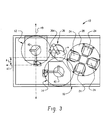
- Figure 3 also illustrates the asymmetrical arrangement of the furnaces 12, 14 of embodiments of the present invention.
- the housing footprint is reduced by an amount corresponding to the overlap A of the two furnaces 12, 14.
- This smaller footprint provides significant advantages since the furnaces are typically mounted in clean rooms where the cost per square foot is significant.
- reducing the size of the thermal processing apparatus means it occupies less clean room space, allowing more thermal processing furnaces to be installed therein. This improves the efficiency and throughput of the facility, while concomitantly reducing costs.
- the vertical furnaces have a width of about 40 inches. If the furnaces were arranged along axis 49, the furnaces themselves would occupy at least 80 inches along the width of the housing 16.
- the overlap A can be about 8 inches, thereby reducing the space occupied by the furnaces along the width of housing by as much as 10%, or even greater in other arrangements.
- the asymmetrical arrangement of the furnaces 12, 14 also optimizes the use of the single wafer transport assembly 36 by allowing the assembly to be disposed at a convenient location to service both vertical furnaces.
Landscapes
- Chemical & Material Sciences (AREA)
- Engineering & Computer Science (AREA)
- Materials Engineering (AREA)
- Metallurgy (AREA)
- Organic Chemistry (AREA)
- General Chemical & Material Sciences (AREA)
- Chemical Kinetics & Catalysis (AREA)
- Mechanical Engineering (AREA)
- Crystallography & Structural Chemistry (AREA)
- Container, Conveyance, Adherence, Positioning, Of Wafer (AREA)
Description
- The present invention relates to a thermal processing furnace for processing semiconductor wafers, and particularly to a vertical type heat processing furnace.
- Thermal processing furnaces, also known as diffusion furnaces, have been widely known and used for many years to perform a variety of semiconductor fabrication processes, including annealing, diffusion, oxidation, and chemical vapor deposition. As a result, these processes are well understood, especially with regard to the impact of process variables on the quality and uniformity of resulting products. Thermal processing furnaces typically employ either a horizontal-type furnace or a vertical-type furnace. For some applications, vertical-type furnaces are preferred because they create less particles during use, thus decreasing the incidence of contamination and wafer waste, they can be easily automated, and they require less floor space because of their relatively small footprint.
- Both conventional types of diffusion furnaces are designed to heat semiconductor wafers to desired temperatures to promote either diffusion of the dopants to a desired depth while maintaining line width smaller than 1 micron, as known, or to perform other conventional processing techniques such as the application of an oxide layer to the wafer or deposition of a chemical vapor layer to the wafer. The heating requirements of the wafer during processing are known and well understood, and thus are closely monitored.
- Conventional vertical-type thermal processing furnaces are designed to support the processing tube within the furnace in the vertical position. The thermal furnace also typically employs a wafer boat assembly which is mounted to appropriate translation mechanisms for moving the wafer boat into and out of the processing tube. A wafer-handling assembly is deployed adjacent and parallel to the wafer-boat assembly to transfer the semiconductor wafers from wafer cassettes, which typically hold up to 100 wafers, to the wafer-boat assembly. The wafer-handling assembly is typically located in a loadlock chamber separate from the chamber housing the process tube, and whose environment is closely controlled by appropriate monitoring structure. The loadlock mounting the wafer-handling assembly can also be isolated from the wafer cassettes, such as by mounting the wafer cassettes in one or more loadlocks that are in selected fluid communication with the wafer-handling assembly loadlock. The serial chain of loadlocks thus allows the precise environmental control necessary during processing to decrease or eliminate the chance of contaminants being formed in the wafer during heating. The loadlocks are typically separated from each other by gate valves that are selectively opened and closed to allow the transfer of a wafer from the wafer cassette to the wafer boat and vice versa.
- In practice, after a vacuum is established in the loadlock chamber mounting the wafer boat, an inert gas such as nitrogen can be introduced to fill the loadlock chamber and to remove air therefrom. This purging of air from the loadlock chamber prevents the formation of natural oxide films on the semiconductor wafer surface. As noted above, the loadlock chamber is connected to other serial loadlocks which house the semiconductor wafer cassettes and the wafer handling assembly, to thus effectuate loading and unloading of the wafer boat in a nitrogen atmosphere. The wafer boat is then loaded with wafers from the wafer cassette via the wafer-handling assembly to form a wafer batch. The batch is then disposed within the furnace, where it undergoes a user-selected process under elevated temperatures. Conventional vertical furnaces of these types are shown and described in U.S. Patent No. 5,217,501 of Fuse et al. and in U.S. Patent No. 5,387,265 of Kakizaki et al.
- US-A-5 464 313 discloses a heat treatment apparatus for semiconductor wafers which includes two heat treatment units which load wafer boats containing wafers from below. Each heat treatment wafer has a delivery section and a wafer transfer mechanism transports wafers between the wafer delivery sections.
- Reference is likewise made to document US 5,187,639.
- Prior furnaces establish an isothermal zone within the process tube that extends between about 20 inches and about 30 inches, where a wafer batch having between about 150 to 200 wafers is disposed. Due to the relatively large thermal mass associated with this wafer batch, the temperature ramp-up rates are relatively small, for example, between about 5 DEG C/min. and about 10 DEG C/min, and the temperature ramp-down rates are relatively small, for example, between about 2.5 DEG C/min. and about 5 DEG C/min. This results in a relatively long thermal cycle per batch, and thus a relatively large thermal budget per wafer.
- Another drawback of these and other conventional vertical-type thermal processing furnaces is that they achieve relatively low throughput because of the increased cycle time per batch. These conventional systems are thus not uniquely situated to accommodate today's ever increasing demands for semiconductor wafers.
- Another drawback of these furnaces is that they incorporate pre-staging loadlock assemblies which form air-free environments for the transfer of wafers to and from the wafer boat. The time involved in venting and purging the loadlocks to achieve these states increases the overall processing time per batch and thus serves to further decrease the throughput of the furnace system.
- Still another drawback is that these furnaces have a relatively large footprint and occupy relatively large amounts of floor space in clean rooms, thus providing for inefficient use of expensive clean room space.
- Due to the foregoing and other shortcomings of prior art vertical-type thermal processing furnaces, it is desirable to provide a vertical-type furnace that provides for relatively high throughput.
- It is also desirable to provide a furnace that achieves improved temperature ramp-up and ramp-down rates.
- It is further desirable to provide a thermal processing furnace that can be easily automated and occupies relatively small floor space.
- Embodiments of the present invention according to claim 1 for a vertical semiconductor wafer processing furnace that includes a single housing having first and second vertical furnaces each having a heating chamber for heat treating a semiconductor wafer. Each vertical furnace includes a wafer support assembly that includes support structure, such as a wafer boat, boat elevator, motor and guide rod, for axially mounting a selected number of semiconductor wafers.
- According to one aspect of the embodiments, a translation element selectively moves one of the support elements along the vertical axis into and out of the process tube, and a wafer transfer element selectively transfers semiconductor wafers to or from one of the support elements. According to one preferred practice, there is a translation element associated with each of the wafer support assemblies for moving the support elements along each longitudinal axis and selectively into the heating chamber.
- According to another aspect of the embodiments, the furnace includes a control element that is responsive to a control signal, for example, a user-generated control signal, for generating a position signal and for transferring the position signal to the translation element to regulate, e.g., initiate, modify or cease, movement of one of the support structures along the axis in response to the position signal. The control element thus independently or simultaneously controls the rate of movement of each support structure. According to one practice, the control element includes a motion controller that operates in cooperation with a host computer that generates the position signal, the support structure. The control signal applied to the control element can be representative of at least one of a selected temperature ramp-up rate condition and a selected temperature ramp-down rate condition.
- According to still another aspect of the embodiments, the translation element can generate a movement signal indicative of the rate of movement of at least one of the first and second support elements, and the control element is responsive to this movement signal and controls the rate of movement of one of the support elements along the longitudinal axis.
- According to still another aspect of the embodiments, each vertical furnace, e.g., the first and second vertical furnaces, includes a heat generating element that transfers heat to each corresponding processing chamber. The control element can independently or simultaneously control the temperature of the first and second processing chambers by regulating the thermal energy output of each heat generating elements. According to one practice, the control element can regulate the heat generating elements to attain a substantially uniform temperature along at least a portion of the chamber to form a substantially isothermal environment.
- According to another aspect, the furnace includes a heating sleeve or envelope that is adapted to control the ambient fluid environment surrounding the support structure, e.g., the wafer boat. The heating sleeve includes a flanged bottom portion that is adapted to sealingly engage a portion of the support element to create a fluid-tight seal forming a loadlock processing assembly. This assembly is coupled to a vertical translation assembly that selectively, vertically moves the processing assembly into the heating chamber of the vertical furnace. According to a preferred embodiment, a heating sleeve is associated with each vertical furnace. Additionally, the heating sleeve can be vertically moved relative to the support structure to engage and disengage repetitively and easily and automatically the heating sleeve relative to the support structure.
- When the heating sleeve is disposed over the support structure and sealingly engages the bottom portion of the support structure, the assembly forms a loadlock processing chamber within which selected processing techniques can be performed. This chamber can be coupled to appropriate fluid manifolding to introduce one or more selected gases to the chamber and to evacuate one or more gases.
- The use of dual heating envelopes and furnaces in a single thermal processing furnace allows the furnace to perform two separate processing techniques separately and independently, thus increasing the furnace's flexibility of use. The furnace further achieves increased ramp-up and ramp-down rates, reducing the total time necessary to process a wafer batch, thus increasing the total furnace throughput. This is all achieved by packaging dual furnaces in a single housing having small dimensions and by employing wafer boats that have increased wafer pitch and that process smaller batch sizes.
- The foregoing and other features and advantages of the invention will be apparent from the following description and apparent from the accompanying drawings, in which like reference characters refer to the same parts throughout the different views. The drawings illustrate embodiments of the invention and, although not to scale, show relative dimensions.
- FIG. 1 is a plan view of the thermal processing furnace.
- FIG. 2 is a perspective view, partly in cross-section, showing the inner portions of the thermal processing furnace of FIG. 1.
- FIG. 3 is a top view of the wafer transfer assembly housed within the thermal processing furnace of FIG. 1, and which further illustrates the asymmetrical furnace arrangement.
-
- Figure 1 illustrates a perspective view of the vertical-type
thermal processing furnace 10 of an embodiment of the present invention illustrating in partly broken view the dualvertical furnaces thermal processing furnace 10 is designed to be compact and to have a relatively small footprint. For example, according to one embodiment of the invention, the furnace can be about 40 inches wide by about 65 inches deep, and has a height of about 96.5 inches. The furnace is typically used to perform a variety of semi-conductive fabrication processes, including annealing, diffusion, oxidation and low and high pressure chemical vapor deposition. - The illustrated
thermal processing furnace 10 includes a mainouter housing 16 that encloses a pair ofvertical furnaces housing 16 includes a plurality ofsides 16A and a front face 16B that includes awafer storage compartment 20. A pair of vertically spacedcarousels compartment 20. These wafers can be unprocessed or processed wafers.Door panels 22 enclose and cover thecompartment 20. As shown, amonitor 30 can be mounted within the front face 16B of thehousing 16 to allow an operator to monitor selected process control parameters, such as the temperature, process time, types of gas and other selected process control parameters. - With reference to Figure 3, the
wafer cassettes 24 are mounted oncarousal 28. A three-axiswafer transfer assembly 36 having amechanical transport arm 36A transports wafer W from a selectedcassette 24 to one of thewafer boats 40 disposed in eachvertical furnace carousal 28 can be selectively rotated to position a selected wafer cassette at a position to allow themechanical transport arm 36 to remove a wafer from or place a wafer on that particular cassette. In this way, the illustratedthermal processing furnace 10 allows for selected control and continuous processing of the wafers during furnace operation. Thetransfer assembly 36 is preferably vertically movable to allow thetransport arm 36 to access thewafer cassettes 24 on either theupper carousel 28 or thelower carousel 26. Those of ordinary skill will readily understand and appreciate the various types of transport assemblies available for use in thermal processing furnaces, as well as the operation of thewafer transfer assembly 36 in conjunction with wafer handling and processing. - FIGS. 1 through 3, and particularly FIG. 2, illustrate the components of the
thermal processing furnace 10 of an embodiment of the present invention. Thevertical furnace 14 includes acylindrical process tube 44 that has aclosed end 44A and an opposed open end 44B. Thecylindrical tube 44 defines aheating chamber 46. Theprocess tube 44 can be formed of any high temperature material such as alumina, silicon carbide, and other ceramic materials, and is preferably composed of quartz. The process tube is surrounded by asuitable heating element 48 that uses resistance-heated elements or RF heated black body cavity susceptors as the primary heat source. This particular type of heat source is simple to implement, well characterized and widely accepted as a reliable technique for stable and uniform control of the furnace temperature. According to one embodiment, theheating element 48 forms part of a heater module that is a vertical oriented, three zone resistive heated unit. The heating elements can be composed of low mass, high temperature metallic wires. The insulation surrounding the heating element can be composed of ceramic fibers of high insulation value and low thermal mass. All are designed for fast responses to temperature changes. The module can also include an air cooling system to help cool theheating chamber 46. Theprocess tube 44 diameter and thus the size of the vertical furnace can be easily scaled to accommodate wafers of varying sizes. - The
heating element 48 is arranged about eachprocess tube 44 to heat the inside of the tube to a predetermined temperature, e.g., 400°C to 1200°C in the case of chemical vapor deposition, or 800°C to 1200°C in the case of oxidation or diffusion. Thecontrol unit 66 can be used to regulate the temperature of theprocess tube 44 according to the exigencies of the processing technique. For example, according to one practice, a temperature sensor, such as an optical pyrometer, can be used to sense the chamber temperature and can be linked to thecontrol unit 66. The heating unit preferably forms an isothermal heating zone within the heating chamber, as is known in the art. - The
housing 16 encloses a wafer support assembly 54 that includes awafer boat 40 supported by aheat insulating stanchion 50. Thebottom portion 54A of the wafer support assembly 54 has an integrally formed and radially outwardly extendingflange plate 54B. The illustrated wafer support assembly 54 is coupled to aboat elevator 58 that slidably engages aguide rod 60. The wafer support assembly is thus selectively vertically movable along the vertical axis of the guide rod to selectively move the wafer support assembly into and out of thefurnace heating chamber 46. - The
vertical furnace 12 is similarly constructed. - The
mechanical transport arm 36A of themechanical transfer assembly 36 selectively moves wafers from a selectedcassette 24 mounted on one of thecarousels wafer boats 40 of eitherfurnace - The wafers are arranged on the wafer boat at predetermined vertical intervals, known as a wafer pitch, and are preferably separated between 5 mm and about 20 mm, and most preferably between about 10 mm and about 20 mm. This selected wafer pitch provides for relatively large spacing between vertically adjacent wafers, which results in better within wafer and wafer-to-wafer temperature uniformities. In contrast, some prior designs typically employ a wafer pitch of between about 3 mm and 5 mm for standard furnace processing.
- A significant advantage of this larger wafer pitch is that it allows for relatively fast temperature ramping of the wafer without suffering wafer uniformity degradation. This larger spacing also relaxes the mechanical tolerances of the
mechanical transport arm 36A during loading and unloading of the wafer boat since the arm has a larger space in which to operate. The smaller wafer batch size of the wafer boats presents a smaller semiconductor mass in which to heat during thermal processing. Consequently, the semiconductor wafers can more easily ramp up and ramp down in temperatures, increasing the overall throughput of the system. - Referring again to FIG. 2, a
servo motor 64 controls the movement of theboat elevator 58 along theguide rod 60. Theservo motor 64 is preferably controlled by thecontrol unit 66, which can include amotion controller 68, via selected signals transferred along electrical lead 70. The illustratedmotion controller 68 is further in electrical communication with ahost computer 74, as illustrated bydata flow pathway 76. Likewise, thecomputer 74 is also in bidirectional communication with a data acquisition stage, which accumulates selected processing data associated with the thermal processing operation of the illustrated furnace. Data can be transferred between thehost computer 74 and the data acquisition stage alongdata flow pathway 78. - The
robot controller 82 is also in bidirectional communication with thecomputer 74 by way ofsignal pathway 80, and also transfers selected control signals alongelectrical lead 86 to thewafer transfer assembly 36. The robot controller thus controls the selected position and relative movement of thetransport arm 36A to remove or load a wafer onto a selectedcassette 24 mounted on one of thecarousels - The
computer 74,motion controller 68,data acquisition stage 72, androbot controller 82 thus form a closed loop feedback control stage that selectively raises and lowers the wafer support assembly as well as controls the relative movement of themechanical transport arm 36A. Those of ordinary skill will appreciate that one or more of the motion controller, data acquisition stage and robot controller can be implemented in hardware and/or software and thus form part ofcomputer 74, rather than provide a separate stage. - The illustrated
furnace 10 further includes aheating sleeve 100 that is dimensioned to seat withinprocess tube 44. Similar in construction to the process tube, theheating sleeve 100 is also formed of a high temperature material, e.g., quartz, having a firstclosed end 100A and an opposedopen end 100B. The sleeveopen end 100B further includes an outwardly extending flange portion 100C. Theheating tube 100 is coupled to asleeve elevator 104 that slidingly engages theguide rod 60 or other suitable guiding structure. Theheating sleeve 100 is movable independently of the wafer support assembly 54. - The relative vertical position of the
heating sleeve 100 can be feedback controlled by themotion controller stage 68 of thecontrol unit 66. For example, themotion controller 68 can be used to selectively actuate theservo motor 64 to raise or lower theheating sleeve 100, the wafer support assembly 54, or both simultaneously. The flange 100C of the heating sleeve is adapted to sealingly engage theflange portion 54B of the wafer support assembly 54 to form a fluid-tight and vacuum-tight seal. Thus, when theheating sleeve 100 is disposed over the wafer boat andstanchion 50 and sealingly engages theflange portion 54B of the wafer support assembly 54, thesleeve 100 forms aloadlock processing chamber 108. Theheating sleeve 100 cooperates with the wafer support assembly to form an ambient control mechanism for controlling the ambient environment of the wafers mounted in thewafer boat 40 exclusive of the environment of theheating chamber 46 of theprocess tube 44. The sleeve thus operates, in one selected position, e.g., when the flange 100C sealingly engagesflange 54B, as a vertically movable loadlock chamber which is selectively disposable within theheating chamber 46. Theheating sleeve 100 can be raised or lowered into theheating chamber 46 along with the wafer support assembly 54, so that the wafers are in a strictly controlled ambient environment during both the temperature ramp-up (heating) or ramp-down (cooling) phase. - Gas manifolding structure can be coupled to the wafer transport assembly 54 and the
heating sleeve 100 to control the fluid environment of theloadlock processing chamber 108 associated withfurnace 14, FIG. 2. For example, according to one embodiment, a small quartz conduit is coupled togas box 112 and to the flange plate of the wafer transport assembly 54 to transport a selected process gas contained within the gas box to the top of theprocess chamber 108. The process gas passes over the wafer boats, through suitable exhaust ports, e.g., located at the bottom of the process chamber, and is exhausted through exhaust ductwork into the gas box exhaust port. The gas box is coupled to an associated gas panel, e.g.,gas panel 112A, and can also be coupled to thecontrol unit 66. Theother gas box 116 and associatedgas panel 116A correspond to the othervertical furnace 12. Those of ordinary skill will recognize that the two gas boxes can be replaced by a single gas box. - The gas introducing pipe allows the passage of a selected process gas into the
process chamber 108. Various process gases can be introduced into the process chamber to dispose selected films upon the semiconductor wafers. For example, oxygen can be introduced into the chamber to form an oxide film, SiH4 can be introduced for forming a polysilicon film, and NH4 and SiH2Cl2 can be introduced to form a silicon nitride film. Moreover, a purge gas such as nitrogen can be selectively introduced to theprocess chamber 108 to remove air therefrom. As is known, the presence of air in the process chamber during the high temperature processing and annealing of the semiconductor wafers disposes a relatively thick and poor quality oxide film upon the semiconductor wafers. In addition, a cleaning gas for removing a natural oxidation film from the wafers can be introduced into theprocess chamber 108. The cleaning gas can be, for example, a plasmaless etching gas such as NF3 and HCl, a reducing gas such as hydrogen, or other appropriate gases. The gas introducing pipe can be formed at an upper or lower portion of theheating sleeve 100, or can be similarly mounted to the wafer transport assembly 54. An exhaust pipe is similarly formed in the heating sleeve or wafer transport assembly to selectively purge theprocess chamber 108 of the introduced gas. Hence, the gas disposed within the heating sleeve can be exhausted through the exhaust pipe, thereby setting the inside of the heating sleeve to a predetermined degree of vacuum, or to remove the gas which has been previously introduced via the gas introducing pipes. - The gas introduced into the process chamber during heating is preferably decomposed by the high temperature environment and deposits upon the exposed surfaces of the semiconductor wafers. Consequently, the gases are introduced into the process chamber in preselected quantities to dispose a film having a selected thickness on the wafer.
- In operation, the
mechanical transport arm 36A of themechanical assembly 36 is feedback controlled by therobot controller 82 to selectively place a wafer on or remove a wafer from thewafer cassette 24 or thewafer boat 40. According to one practice, while the vertical position of the wafer support assembly is varied, themechanical transport arm 36A loads thewafer boat 40 with a wafer batch, which includes a selected number of wafers to be processed. As mentioned above, the batch size is generally about half the size of conventional wafer batches. Thetransport arm 36A loads thewafer boat 40 by removing wafers from selectedwafer cassettes 24. Once thewafer boat 40 has been loaded, themotion controller stage 68 of thecontrol unit 66 outputs a selected signal to theservomotor 64 to lower theheating sleeve 100 along theguide rod 60 until the flange 100C located at theopen end 100B of thesleeve 100 sealingly engages and mates with theflange plate 54B of the wafer transfer assembly 54. Alternatively, the servomotor can raise the flange plate of the wafer assembly unit it sealingly engages the heating sleeve flange 100C. If desired, a selected gas is introduced to theloadlock process chamber 108 formed by theheating sleeve 100 and the wafer support assembly. Theheating sleeve 100 and/or wafer support assembly 54 are then selectively raised and introduced to theheating chamber 46 of theprocess tube 44. The wafer batch is heated by the heating elements to a selected process temperature depending upon the particular process technique to be performed, and at a relatively accelerated temperature ramp-up rate. The process gas is supplied to form a film on the wafer. - After a user selected duration in the isothermal heating zone of the
furnace 14, the sleeve and transport assembly 54 are lowered and removed from theheating chamber 46. The wafers are left in theloadlock process chamber 108 where they are cooled at a relatively fast temperature ramp-down rate. The wafer temperature is decreased by radiation cooling (although direct cooling techniques can also be employed) until the temperature of the wafers attains a desired value, e.g., 50°C or less. After the wafers are cooled, thecomputer 74 actuates theservomotor 64 to raise theheating sleeve 100 relative to the wafer support assembly 54 to break or disengage the sealing engagement therebetween. The processed wafers stored on thewafer boat 40 are then successively removed by the wafer transfer assembly and conveyed to the wafer cassettes. - Because of the smaller batch sizes of the wafer boats as well as the increased wafer pitch, the temperature ramp-up and ramp-down rates are significantly enhanced. For example, significant increases in the temperature ramp-up rates can be achieved and approach or exceed 100°C per minute. Likewise, the temperature ramp-down rates are further enhanced and approach or exceed 50°C per minute. For practical applications, however, a ramp-up rate between about 30°C and about 75°C per minute and a temperature ramp-down rate of about 15°C per minute and about 40°C per minute are sufficient. These increased ramp-up and ramp-down temperature rates significantly increase the throughput of the
thermal processing furnace 10 by significantly reducing the overall batch processing time. The temperature ramp-down rates can be further influenced by the introduction of a cooling jet stream that flows across the surfaces of the wafers to remove heat therefrom. For example, a non-oxidizing inert gas such as nitrogen can be introduced to thechamber 108, or in the situation where thesleeve 100 has been disengaged from the wafer transport assembly 54 applied directly across the wafers, to further shorten the wafer cooling time. FIG. 2 thus illustrates a wafer support assembly 54 and aheating sleeve 100 which are selectively disposable within aheating chamber 46 of a furnace. Although not shown, similar heating and processing structure exists and is associated with thevertical furnace 12. For example, thevertical furnace 12 includes aprocess tube 44 surrounded by selected heating elements. A selectively verticallymovable heating sleeve 100 and wafer transport assembly 54 are also associated therewith and selectively disposable within the process tube. - Embodiments of the present invention thus utilize a single host computer (or a plurality of integrated control stages, FIG. 2) and a wafer transfer assembly to selectively load a pair of wafer boats which are individually and independently movable into and out of a corresponding
vertical furnace thermal processing furnace 10 of a preferred embodiment of the present invention thus houses a pair of process tubes, a pair of heating sleeves, and a pair of wafer support assemblies 54. Thevertical furnaces furnace 10 and to thus provide a relatively small footprint. - The thermal processing furnace of embodiments of the present invention are capable of achieving enhanced temperature ramp-up and ramp-down rates without sacrificing throughput in a relatively small housing having a relatively small footprint. Because the furnace of embodiments of the present invention achieves enhanced heating and cooling of the wafers, the thermal budget required for each batch is significantly reduced. This translates into significant cost savings and increased throughput.
- Other advantages of embodiments of the present invention include the use of dual vertical furnaces that are capable of performing, if desired, two separate semiconductor processing techniques on individual wafer batches independent of each other in each furnace. For example, an oxide film can be formed on one batch of wafers in one of the furnaces while a polysilicon film can be deposited on the other batch in the other furnace. This multi-processing multiple furnace setup in a single housing provides for a relatively flexible thermal processing furnace that enjoys significant advantages over heretofore known thermal processing furnaces. Furthermore, the use of dual furnaces in a single housing arrangement reduces the overall processing time of the wafers, thereby increasing the throughput of the system. For example, one wafer batch can be processed while the other wafer batch, disposed in the other furnace, can be cooled, unloaded and another wafer batch loaded. This dual furnace arrangement can thereby cut the total processing time of the wafer batches by as much as 25%, or greater, while concomitantly reducing operator interface requirements.
- The dual vertical furnace arrangement, which is incorporated into one package and which minimizes floor space, allows the dual furnaces to share a single wafer mechanical transport assembly. This results in a more efficient use of the transport assembly, since in conventional systems it is typically used less than about 25% of the total process time.
- Figure 3 also illustrates the asymmetrical arrangement of the
furnaces vertical furnaces housing 16, e.g., would be symmetrical aboutboundary line 47 and colinear alongaxis 49. This arrangement would provide for a larger housing footprint. By moving one of the furnaces away fromaxis 49 and asymmetrically arranging the furnace within the housing, e.g., the furnaces are no longer symmetrical aboutboundary line 47, the housing footprint is reduced by an amount corresponding to the overlap A of the twofurnaces - According to one practice, the vertical furnaces have a width of about 40 inches. If the furnaces were arranged along
axis 49, the furnaces themselves would occupy at least 80 inches along the width of thehousing 16. When thefurnaces - The asymmetrical arrangement of the
furnaces wafer transport assembly 36 by allowing the assembly to be disposed at a convenient location to service both vertical furnaces. - Since certain changes may be made in the above constructions without departing from the scope of the invention, it is intended that all matter contained in the above description or shown in the accompanying drawings be interpreted as illustrative and not in a limiting sense.
Claims (8)
- A vertical semiconductor wafer processing furnace, comprising a single housing (16) having
first vertical heating means (12) extending along a first longitudinal axis including means forming a first heating chamber (46) for heat treating semiconductor wafers (W),
second vertical heating means (14) extending along a second longitudinal axis including means forming a second heating chamber (44) for heat treating semiconductor wafers (W),
a first wafer support assembly (54) including first support means for axially mounting a selected number of semiconductor wafers,
a second wafer support assembly including second support means for axially mounting a selected number of semiconductor wafers,
translation means (64) for selectively moving at least one of said first and second support means along said corresponding longitudinal axis, and
wafer transfer means (36) associated with said first and second support means for selectively transferring semiconductor wafers to or from at least one of said first and second support means, characterised in that
said second vertical heating means is asymmetrically disposed about a horizontal boundary line (47) of said first vertical heating means within said single housing. - The furnace of claim 1 further comprising control means (66) which is designed to be responsive to a control signal for generating a position signal (70) and for transferring said position signal to said translation means (64), said translation means moving at least one of said first and second support means along said corresponding longitudinal axis in response to said position signal.
- The furnace of claim 2, wherein said translation means (64) comprises first translation means (64) associated with said first wafer support structure (54) for moving said first support means along said first longitudinal axis in response to a first position signal (70), and second translation means (64) associated with said second wafer support structure (54) for moving said second support means along said second longitudinal axis in response to a second position signal (70).
- The furnace of claim 1 further comprising control means (66) which is designed to control independently the temperature of each of said first and second heating chambers.
- The furnace of any preceding claim wherein each of said first and second wafer support assembly (54) includes a wafer boat (40) coupled to a boat elevator (58) and means (64) for moving said boat elevator in a vertical direction along said corresponding axis.
- The furnace of any preceding claim wherein said first vertical heating means includes ambient control means (100) for selectively controlling the ambient gas surrounding the first support means (54), and said ambient control means is disposed within said first heating chamber (46).
- The furnace of claim 6, wherein said ambient control means includes a heating sleeve (100) associated with said first heating means (12), and means for selectively moving said heating sleeve along said first axis into and out of said first heating chamber (46), and said heating sleeve is disposed over and in sealing connection with said first support means.
- The furnace of claim 7, wherein said heating sleeve (100) is designed to be movable along said first axis together with or independently of said first support means.
Applications Claiming Priority (2)
| Application Number | Priority Date | Filing Date | Title |
|---|---|---|---|
| US2144296P | 1996-07-10 | 1996-07-10 | |
| US21442 | 1999-10-08 |
Publications (3)
| Publication Number | Publication Date |
|---|---|
| EP0818807A2 EP0818807A2 (en) | 1998-01-14 |
| EP0818807A3 EP0818807A3 (en) | 2000-04-05 |
| EP0818807B1 true EP0818807B1 (en) | 2005-08-10 |
Family
ID=21804261
Family Applications (1)
| Application Number | Title | Priority Date | Filing Date |
|---|---|---|---|
| EP97304647A Expired - Lifetime EP0818807B1 (en) | 1996-07-10 | 1997-06-27 | Dual vertical thermal processing furnace |
Country Status (6)
| Country | Link |
|---|---|
| US (2) | US5820366A (en) |
| EP (1) | EP0818807B1 (en) |
| JP (1) | JP4174837B2 (en) |
| CN (1) | CN1109779C (en) |
| DE (1) | DE69733923T2 (en) |
| TW (1) | TW379359B (en) |
Families Citing this family (329)
| Publication number | Priority date | Publication date | Assignee | Title |
|---|---|---|---|---|
| US5820366A (en) * | 1996-07-10 | 1998-10-13 | Eaton Corporation | Dual vertical thermal processing furnace |
| JP3396431B2 (en) * | 1998-08-10 | 2003-04-14 | 東京エレクトロン株式会社 | Oxidation treatment method and oxidation treatment device |
| JP3664897B2 (en) | 1998-11-18 | 2005-06-29 | 東京エレクトロン株式会社 | Vertical heat treatment equipment |
| US6294394B1 (en) * | 1999-07-01 | 2001-09-25 | Voyan Technology | Ramp rate limiter to control stress during ramping |
| JP4578615B2 (en) * | 1999-07-21 | 2010-11-10 | 東京エレクトロン株式会社 | Heat treatment equipment |
| US6410455B1 (en) | 1999-11-30 | 2002-06-25 | Wafermasters, Inc. | Wafer processing system |
| US6452196B1 (en) | 1999-12-20 | 2002-09-17 | Axcelis Technologies, Inc. | Power supply hardening for ion beam systems |
| US6610968B1 (en) * | 2000-09-27 | 2003-08-26 | Axcelis Technologies | System and method for controlling movement of a workpiece in a thermal processing system |
| EP1354028B1 (en) * | 2001-01-26 | 2007-09-19 | Liconic Ag | Air-conditioned storage cupboard |
| KR100443121B1 (en) * | 2001-11-29 | 2004-08-04 | 삼성전자주식회사 | Method for processing of semiconductor and apparatus for processing of semiconductor |
| JP4132932B2 (en) * | 2002-04-12 | 2008-08-13 | 東京エレクトロン株式会社 | Vertical heat treatment equipment |
| US7022192B2 (en) * | 2002-09-04 | 2006-04-04 | Tokyo Electron Limited | Semiconductor wafer susceptor |
| AU2003277790A1 (en) | 2002-11-15 | 2004-06-15 | Unaxis Balzers Ag | Apparatus for vacuum treating two dimensionally extended substrates and method for manufacturing such substrates |
| KR100491161B1 (en) | 2002-11-26 | 2005-05-24 | 주식회사 테라세미콘 | Semiconductor manufacturing system for thermal process |
| US6799940B2 (en) | 2002-12-05 | 2004-10-05 | Tokyo Electron Limited | Removable semiconductor wafer susceptor |
| US7214274B2 (en) * | 2003-03-17 | 2007-05-08 | Tokyo Electron Limited | Method and apparatus for thermally insulating adjacent temperature controlled processing chambers |
| DE10329868A1 (en) * | 2003-07-02 | 2005-01-20 | Dynamic Microsystems Semiconductor Equipment Gmbh | Storage system for wafers |
| US6855916B1 (en) | 2003-12-10 | 2005-02-15 | Axcelis Technologies, Inc. | Wafer temperature trajectory control method for high temperature ramp rate applications using dynamic predictive thermal modeling |
| CN100356505C (en) * | 2003-12-26 | 2007-12-19 | 清华大学 | Fast semiconductor heat-treating facility with vertical heat treating chamber |
| DE102004024207B4 (en) * | 2004-05-10 | 2016-03-24 | Ihp Gmbh - Innovations For High Performance Microelectronics / Leibniz-Institut Für Innovative Mikroelektronik | A method and apparatus for low temperature epitaxy on a variety of semiconductor substrates |
| US7205231B2 (en) * | 2004-10-29 | 2007-04-17 | Axcelis Technologies, Inc. | Method for in-situ uniformity optimization in a rapid thermal processing system |
| US7371998B2 (en) * | 2006-07-05 | 2008-05-13 | Semitool, Inc. | Thermal wafer processor |
| EP1972874B1 (en) * | 2007-03-20 | 2019-02-13 | Liconic Ag | Automated substance warehouse |
| JP4464993B2 (en) * | 2007-06-29 | 2010-05-19 | 東京エレクトロン株式会社 | Substrate processing system |
| US7806684B2 (en) * | 2007-10-02 | 2010-10-05 | United Microelectronics Corp. | Method of semiconductor process and semiconductor apparatus system |
| CN101414570B (en) * | 2007-10-18 | 2011-11-23 | 联华电子股份有限公司 | Semiconductor process method and semiconductor device system |
| KR100945912B1 (en) * | 2008-01-10 | 2010-03-05 | 주식회사 비아트론 | Heat treatment device for semiconductor device |
| JP5274213B2 (en) * | 2008-11-14 | 2013-08-28 | 株式会社日立国際電気 | Substrate processing apparatus, semiconductor device manufacturing method, and temperature control method |
| CN102080264B (en) * | 2009-11-26 | 2012-12-12 | 中科晶电信息材料(北京)有限公司 | Wafer vertically-annealing method and device |
| TWI408327B (en) * | 2010-12-03 | 2013-09-11 | Tangteck Equipment Inc | Method for heating and cooling diffusion furnace device |
| CN102094248B (en) * | 2010-12-31 | 2012-07-11 | 东莞市中镓半导体科技有限公司 | Annealing device and method |
| US20120171002A1 (en) * | 2011-01-05 | 2012-07-05 | Electro Scientific Industries, Inc | Apparatus and method for transferring a substrate |
| US20130023129A1 (en) | 2011-07-20 | 2013-01-24 | Asm America, Inc. | Pressure transmitter for a semiconductor processing environment |
| US9048271B2 (en) | 2011-09-29 | 2015-06-02 | Asm International N.V. | Modular semiconductor processing system |
| TW201327712A (en) * | 2011-11-01 | 2013-07-01 | 因特瓦克公司 | System architecture for processing solar cell wafers with plasma |
| CN104364888B (en) * | 2012-05-28 | 2017-02-22 | 株式会社日立国际电气 | Substrate processing apparatus, temperature measurement system, temperature measurement method for processing apparatus, conveying apparatus, and recording medium |
| US10714315B2 (en) | 2012-10-12 | 2020-07-14 | Asm Ip Holdings B.V. | Semiconductor reaction chamber showerhead |
| US20160376700A1 (en) | 2013-02-01 | 2016-12-29 | Asm Ip Holding B.V. | System for treatment of deposition reactor |
| CN103938273A (en) * | 2014-02-21 | 2014-07-23 | 上海华力微电子有限公司 | Double diffusion furnace tube system |
| US11015245B2 (en) | 2014-03-19 | 2021-05-25 | Asm Ip Holding B.V. | Gas-phase reactor and system having exhaust plenum and components thereof |
| CN105088334B (en) * | 2014-04-28 | 2018-01-09 | 北京北方华创微电子装备有限公司 | Cover device and process equipment |
| US10858737B2 (en) | 2014-07-28 | 2020-12-08 | Asm Ip Holding B.V. | Showerhead assembly and components thereof |
| US10941490B2 (en) | 2014-10-07 | 2021-03-09 | Asm Ip Holding B.V. | Multiple temperature range susceptor, assembly, reactor and system including the susceptor, and methods of using the same |
| US10276355B2 (en) | 2015-03-12 | 2019-04-30 | Asm Ip Holding B.V. | Multi-zone reactor, system including the reactor, and method of using the same |
| KR101720620B1 (en) * | 2015-04-21 | 2017-03-28 | 주식회사 유진테크 | Substrate Processing Apparatus and Method of Cleaning Chamber |
| US10458018B2 (en) | 2015-06-26 | 2019-10-29 | Asm Ip Holding B.V. | Structures including metal carbide material, devices including the structures, and methods of forming same |
| US10211308B2 (en) | 2015-10-21 | 2019-02-19 | Asm Ip Holding B.V. | NbMC layers |
| US11139308B2 (en) | 2015-12-29 | 2021-10-05 | Asm Ip Holding B.V. | Atomic layer deposition of III-V compounds to form V-NAND devices |
| US10529554B2 (en) | 2016-02-19 | 2020-01-07 | Asm Ip Holding B.V. | Method for forming silicon nitride film selectively on sidewalls or flat surfaces of trenches |
| US10343920B2 (en) | 2016-03-18 | 2019-07-09 | Asm Ip Holding B.V. | Aligned carbon nanotubes |
| US10367080B2 (en) | 2016-05-02 | 2019-07-30 | Asm Ip Holding B.V. | Method of forming a germanium oxynitride film |
| US11453943B2 (en) | 2016-05-25 | 2022-09-27 | Asm Ip Holding B.V. | Method for forming carbon-containing silicon/metal oxide or nitride film by ALD using silicon precursor and hydrocarbon precursor |
| US9859151B1 (en) | 2016-07-08 | 2018-01-02 | Asm Ip Holding B.V. | Selective film deposition method to form air gaps |
| US10612137B2 (en) | 2016-07-08 | 2020-04-07 | Asm Ip Holdings B.V. | Organic reactants for atomic layer deposition |
| US9812320B1 (en) | 2016-07-28 | 2017-11-07 | Asm Ip Holding B.V. | Method and apparatus for filling a gap |
| KR102532607B1 (en) | 2016-07-28 | 2023-05-15 | 에이에스엠 아이피 홀딩 비.브이. | Substrate processing apparatus and method of operating the same |
| US9887082B1 (en) | 2016-07-28 | 2018-02-06 | Asm Ip Holding B.V. | Method and apparatus for filling a gap |
| US11532757B2 (en) | 2016-10-27 | 2022-12-20 | Asm Ip Holding B.V. | Deposition of charge trapping layers |
| US10714350B2 (en) | 2016-11-01 | 2020-07-14 | ASM IP Holdings, B.V. | Methods for forming a transition metal niobium nitride film on a substrate by atomic layer deposition and related semiconductor device structures |
| KR102546317B1 (en) | 2016-11-15 | 2023-06-21 | 에이에스엠 아이피 홀딩 비.브이. | Gas supply unit and substrate processing apparatus including the same |
| KR102762543B1 (en) | 2016-12-14 | 2025-02-05 | 에이에스엠 아이피 홀딩 비.브이. | Substrate processing apparatus |
| US11447861B2 (en) | 2016-12-15 | 2022-09-20 | Asm Ip Holding B.V. | Sequential infiltration synthesis apparatus and a method of forming a patterned structure |
| US11581186B2 (en) | 2016-12-15 | 2023-02-14 | Asm Ip Holding B.V. | Sequential infiltration synthesis apparatus |
| KR102700194B1 (en) | 2016-12-19 | 2024-08-28 | 에이에스엠 아이피 홀딩 비.브이. | Substrate processing apparatus |
| US10269558B2 (en) | 2016-12-22 | 2019-04-23 | Asm Ip Holding B.V. | Method of forming a structure on a substrate |
| US11390950B2 (en) | 2017-01-10 | 2022-07-19 | Asm Ip Holding B.V. | Reactor system and method to reduce residue buildup during a film deposition process |
| US10468261B2 (en) | 2017-02-15 | 2019-11-05 | Asm Ip Holding B.V. | Methods for forming a metallic film on a substrate by cyclical deposition and related semiconductor device structures |
| US10529563B2 (en) | 2017-03-29 | 2020-01-07 | Asm Ip Holdings B.V. | Method for forming doped metal oxide films on a substrate by cyclical deposition and related semiconductor device structures |
| US10770286B2 (en) | 2017-05-08 | 2020-09-08 | Asm Ip Holdings B.V. | Methods for selectively forming a silicon nitride film on a substrate and related semiconductor device structures |
| US12040200B2 (en) | 2017-06-20 | 2024-07-16 | Asm Ip Holding B.V. | Semiconductor processing apparatus and methods for calibrating a semiconductor processing apparatus |
| US11306395B2 (en) | 2017-06-28 | 2022-04-19 | Asm Ip Holding B.V. | Methods for depositing a transition metal nitride film on a substrate by atomic layer deposition and related deposition apparatus |
| TWI794238B (en) | 2017-07-13 | 2023-03-01 | 荷蘭商Asm智慧財產控股公司 | Apparatus and method for removal of oxide and carbon from semiconductor films in a single processing chamber |
| KR20190009245A (en) | 2017-07-18 | 2019-01-28 | 에이에스엠 아이피 홀딩 비.브이. | Methods for forming a semiconductor device structure and related semiconductor device structures |
| US11018002B2 (en) | 2017-07-19 | 2021-05-25 | Asm Ip Holding B.V. | Method for selectively depositing a Group IV semiconductor and related semiconductor device structures |
| US11374112B2 (en) | 2017-07-19 | 2022-06-28 | Asm Ip Holding B.V. | Method for depositing a group IV semiconductor and related semiconductor device structures |
| US10541333B2 (en) | 2017-07-19 | 2020-01-21 | Asm Ip Holding B.V. | Method for depositing a group IV semiconductor and related semiconductor device structures |
| US10590535B2 (en) | 2017-07-26 | 2020-03-17 | Asm Ip Holdings B.V. | Chemical treatment, deposition and/or infiltration apparatus and method for using the same |
| TWI815813B (en) | 2017-08-04 | 2023-09-21 | 荷蘭商Asm智慧財產控股公司 | Showerhead assembly for distributing a gas within a reaction chamber |
| US10770336B2 (en) | 2017-08-08 | 2020-09-08 | Asm Ip Holding B.V. | Substrate lift mechanism and reactor including same |
| US10692741B2 (en) | 2017-08-08 | 2020-06-23 | Asm Ip Holdings B.V. | Radiation shield |
| US11139191B2 (en) | 2017-08-09 | 2021-10-05 | Asm Ip Holding B.V. | Storage apparatus for storing cassettes for substrates and processing apparatus equipped therewith |
| US11769682B2 (en) | 2017-08-09 | 2023-09-26 | Asm Ip Holding B.V. | Storage apparatus for storing cassettes for substrates and processing apparatus equipped therewith |
| US11830730B2 (en) | 2017-08-29 | 2023-11-28 | Asm Ip Holding B.V. | Layer forming method and apparatus |
| KR102491945B1 (en) | 2017-08-30 | 2023-01-26 | 에이에스엠 아이피 홀딩 비.브이. | Substrate processing apparatus |
| US11056344B2 (en) | 2017-08-30 | 2021-07-06 | Asm Ip Holding B.V. | Layer forming method |
| US11295980B2 (en) | 2017-08-30 | 2022-04-05 | Asm Ip Holding B.V. | Methods for depositing a molybdenum metal film over a dielectric surface of a substrate by a cyclical deposition process and related semiconductor device structures |
| US10658205B2 (en) | 2017-09-28 | 2020-05-19 | Asm Ip Holdings B.V. | Chemical dispensing apparatus and methods for dispensing a chemical to a reaction chamber |
| US10403504B2 (en) | 2017-10-05 | 2019-09-03 | Asm Ip Holding B.V. | Method for selectively depositing a metallic film on a substrate |
| US10923344B2 (en) | 2017-10-30 | 2021-02-16 | Asm Ip Holding B.V. | Methods for forming a semiconductor structure and related semiconductor structures |
| US11022879B2 (en) | 2017-11-24 | 2021-06-01 | Asm Ip Holding B.V. | Method of forming an enhanced unexposed photoresist layer |
| TWI791689B (en) | 2017-11-27 | 2023-02-11 | 荷蘭商Asm智慧財產控股私人有限公司 | Apparatus including a clean mini environment |
| WO2019103613A1 (en) | 2017-11-27 | 2019-05-31 | Asm Ip Holding B.V. | A storage device for storing wafer cassettes for use with a batch furnace |
| US10872771B2 (en) | 2018-01-16 | 2020-12-22 | Asm Ip Holding B. V. | Method for depositing a material film on a substrate within a reaction chamber by a cyclical deposition process and related device structures |
| TWI799494B (en) | 2018-01-19 | 2023-04-21 | 荷蘭商Asm 智慧財產控股公司 | Deposition method |
| US11482412B2 (en) | 2018-01-19 | 2022-10-25 | Asm Ip Holding B.V. | Method for depositing a gap-fill layer by plasma-assisted deposition |
| US11081345B2 (en) | 2018-02-06 | 2021-08-03 | Asm Ip Holding B.V. | Method of post-deposition treatment for silicon oxide film |
| WO2019158960A1 (en) | 2018-02-14 | 2019-08-22 | Asm Ip Holding B.V. | A method for depositing a ruthenium-containing film on a substrate by a cyclical deposition process |
| US10896820B2 (en) | 2018-02-14 | 2021-01-19 | Asm Ip Holding B.V. | Method for depositing a ruthenium-containing film on a substrate by a cyclical deposition process |
| US10731249B2 (en) | 2018-02-15 | 2020-08-04 | Asm Ip Holding B.V. | Method of forming a transition metal containing film on a substrate by a cyclical deposition process, a method for supplying a transition metal halide compound to a reaction chamber, and related vapor deposition apparatus |
| KR102636427B1 (en) | 2018-02-20 | 2024-02-13 | 에이에스엠 아이피 홀딩 비.브이. | Substrate processing method and apparatus |
| US10975470B2 (en) | 2018-02-23 | 2021-04-13 | Asm Ip Holding B.V. | Apparatus for detecting or monitoring for a chemical precursor in a high temperature environment |
| US11473195B2 (en) | 2018-03-01 | 2022-10-18 | Asm Ip Holding B.V. | Semiconductor processing apparatus and a method for processing a substrate |
| US11629406B2 (en) | 2018-03-09 | 2023-04-18 | Asm Ip Holding B.V. | Semiconductor processing apparatus comprising one or more pyrometers for measuring a temperature of a substrate during transfer of the substrate |
| US11114283B2 (en) | 2018-03-16 | 2021-09-07 | Asm Ip Holding B.V. | Reactor, system including the reactor, and methods of manufacturing and using same |
| KR102646467B1 (en) | 2018-03-27 | 2024-03-11 | 에이에스엠 아이피 홀딩 비.브이. | Method of forming an electrode on a substrate and a semiconductor device structure including an electrode |
| US11088002B2 (en) | 2018-03-29 | 2021-08-10 | Asm Ip Holding B.V. | Substrate rack and a substrate processing system and method |
| US11230766B2 (en) | 2018-03-29 | 2022-01-25 | Asm Ip Holding B.V. | Substrate processing apparatus and method |
| KR102600229B1 (en) | 2018-04-09 | 2023-11-10 | 에이에스엠 아이피 홀딩 비.브이. | Substrate supporting device, substrate processing apparatus including the same and substrate processing method |
| KR101930456B1 (en) * | 2018-05-03 | 2018-12-18 | 주식회사 유진테크 | System for processing substrate |
| TWI843623B (en) | 2018-05-08 | 2024-05-21 | 荷蘭商Asm Ip私人控股有限公司 | Methods for depositing an oxide film on a substrate by a cyclical deposition process and related device structures |
| US12025484B2 (en) | 2018-05-08 | 2024-07-02 | Asm Ip Holding B.V. | Thin film forming method |
| US12272527B2 (en) | 2018-05-09 | 2025-04-08 | Asm Ip Holding B.V. | Apparatus for use with hydrogen radicals and method of using same |
| KR102596988B1 (en) | 2018-05-28 | 2023-10-31 | 에이에스엠 아이피 홀딩 비.브이. | Method of processing a substrate and a device manufactured by the same |
| US11718913B2 (en) | 2018-06-04 | 2023-08-08 | Asm Ip Holding B.V. | Gas distribution system and reactor system including same |
| TWI840362B (en) | 2018-06-04 | 2024-05-01 | 荷蘭商Asm Ip私人控股有限公司 | Wafer handling chamber with moisture reduction |
| US11286562B2 (en) | 2018-06-08 | 2022-03-29 | Asm Ip Holding B.V. | Gas-phase chemical reactor and method of using same |
| KR102568797B1 (en) | 2018-06-21 | 2023-08-21 | 에이에스엠 아이피 홀딩 비.브이. | Substrate processing system |
| US10797133B2 (en) | 2018-06-21 | 2020-10-06 | Asm Ip Holding B.V. | Method for depositing a phosphorus doped silicon arsenide film and related semiconductor device structures |
| KR20250134000A (en) | 2018-06-27 | 2025-09-09 | 에이에스엠 아이피 홀딩 비.브이. | Cyclic deposition methods for forming metal-containing material and films and structures including the metal-containing material |
| WO2020003000A1 (en) | 2018-06-27 | 2020-01-02 | Asm Ip Holding B.V. | Cyclic deposition methods for forming metal-containing material and films and structures including the metal-containing material |
| US10612136B2 (en) | 2018-06-29 | 2020-04-07 | ASM IP Holding, B.V. | Temperature-controlled flange and reactor system including same |
| US10388513B1 (en) | 2018-07-03 | 2019-08-20 | Asm Ip Holding B.V. | Method for depositing silicon-free carbon-containing film as gap-fill layer by pulse plasma-assisted deposition |
| US10755922B2 (en) | 2018-07-03 | 2020-08-25 | Asm Ip Holding B.V. | Method for depositing silicon-free carbon-containing film as gap-fill layer by pulse plasma-assisted deposition |
| US11053591B2 (en) | 2018-08-06 | 2021-07-06 | Asm Ip Holding B.V. | Multi-port gas injection system and reactor system including same |
| US11430674B2 (en) | 2018-08-22 | 2022-08-30 | Asm Ip Holding B.V. | Sensor array, apparatus for dispensing a vapor phase reactant to a reaction chamber and related methods |
| US11024523B2 (en) | 2018-09-11 | 2021-06-01 | Asm Ip Holding B.V. | Substrate processing apparatus and method |
| KR102707956B1 (en) | 2018-09-11 | 2024-09-19 | 에이에스엠 아이피 홀딩 비.브이. | Method for deposition of a thin film |
| US10998205B2 (en) * | 2018-09-14 | 2021-05-04 | Kokusai Electric Corporation | Substrate processing apparatus and manufacturing method of semiconductor device |
| US11049751B2 (en) | 2018-09-14 | 2021-06-29 | Asm Ip Holding B.V. | Cassette supply system to store and handle cassettes and processing apparatus equipped therewith |
| CN110970344B (en) | 2018-10-01 | 2024-10-25 | Asmip控股有限公司 | Substrate holding device, system including the same and method of using the same |
| US11232963B2 (en) | 2018-10-03 | 2022-01-25 | Asm Ip Holding B.V. | Substrate processing apparatus and method |
| KR102592699B1 (en) | 2018-10-08 | 2023-10-23 | 에이에스엠 아이피 홀딩 비.브이. | Substrate support unit and apparatuses for depositing thin film and processing the substrate including the same |
| KR102546322B1 (en) | 2018-10-19 | 2023-06-21 | 에이에스엠 아이피 홀딩 비.브이. | Substrate processing apparatus and substrate processing method |
| KR102605121B1 (en) | 2018-10-19 | 2023-11-23 | 에이에스엠 아이피 홀딩 비.브이. | Substrate processing apparatus and substrate processing method |
| USD948463S1 (en) | 2018-10-24 | 2022-04-12 | Asm Ip Holding B.V. | Susceptor for semiconductor substrate supporting apparatus |
| US12378665B2 (en) | 2018-10-26 | 2025-08-05 | Asm Ip Holding B.V. | High temperature coatings for a preclean and etch apparatus and related methods |
| US11087997B2 (en) | 2018-10-31 | 2021-08-10 | Asm Ip Holding B.V. | Substrate processing apparatus for processing substrates |
| KR102748291B1 (en) | 2018-11-02 | 2024-12-31 | 에이에스엠 아이피 홀딩 비.브이. | Substrate support unit and substrate processing apparatus including the same |
| US11572620B2 (en) | 2018-11-06 | 2023-02-07 | Asm Ip Holding B.V. | Methods for selectively depositing an amorphous silicon film on a substrate |
| US11031242B2 (en) | 2018-11-07 | 2021-06-08 | Asm Ip Holding B.V. | Methods for depositing a boron doped silicon germanium film |
| US10847366B2 (en) | 2018-11-16 | 2020-11-24 | Asm Ip Holding B.V. | Methods for depositing a transition metal chalcogenide film on a substrate by a cyclical deposition process |
| US10818758B2 (en) | 2018-11-16 | 2020-10-27 | Asm Ip Holding B.V. | Methods for forming a metal silicate film on a substrate in a reaction chamber and related semiconductor device structures |
| US12040199B2 (en) | 2018-11-28 | 2024-07-16 | Asm Ip Holding B.V. | Substrate processing apparatus for processing substrates |
| US11217444B2 (en) | 2018-11-30 | 2022-01-04 | Asm Ip Holding B.V. | Method for forming an ultraviolet radiation responsive metal oxide-containing film |
| KR102636428B1 (en) | 2018-12-04 | 2024-02-13 | 에이에스엠 아이피 홀딩 비.브이. | A method for cleaning a substrate processing apparatus |
| US11703229B2 (en) * | 2018-12-05 | 2023-07-18 | Yi-Ming Hung | Temperature adjustment apparatus for high temperature oven |
| US11158513B2 (en) | 2018-12-13 | 2021-10-26 | Asm Ip Holding B.V. | Methods for forming a rhenium-containing film on a substrate by a cyclical deposition process and related semiconductor device structures |
| JP7504584B2 (en) | 2018-12-14 | 2024-06-24 | エーエスエム・アイピー・ホールディング・ベー・フェー | Method and system for forming device structures using selective deposition of gallium nitride - Patents.com |
| TWI866480B (en) | 2019-01-17 | 2024-12-11 | 荷蘭商Asm Ip 私人控股有限公司 | Methods of forming a transition metal containing film on a substrate by a cyclical deposition process |
| KR102727227B1 (en) | 2019-01-22 | 2024-11-07 | 에이에스엠 아이피 홀딩 비.브이. | Semiconductor processing device |
| CN111524788B (en) | 2019-02-01 | 2023-11-24 | Asm Ip私人控股有限公司 | Method for forming topologically selective films of silicon oxide |
| KR102638425B1 (en) | 2019-02-20 | 2024-02-21 | 에이에스엠 아이피 홀딩 비.브이. | Method and apparatus for filling a recess formed within a substrate surface |
| KR102626263B1 (en) | 2019-02-20 | 2024-01-16 | 에이에스엠 아이피 홀딩 비.브이. | Cyclical deposition method including treatment step and apparatus for same |
| TWI845607B (en) | 2019-02-20 | 2024-06-21 | 荷蘭商Asm Ip私人控股有限公司 | Cyclical deposition method and apparatus for filling a recess formed within a substrate surface |
| TWI838458B (en) | 2019-02-20 | 2024-04-11 | 荷蘭商Asm Ip私人控股有限公司 | Apparatus and methods for plug fill deposition in 3-d nand applications |
| TWI842826B (en) | 2019-02-22 | 2024-05-21 | 荷蘭商Asm Ip私人控股有限公司 | Substrate processing apparatus and method for processing substrate |
| KR102782593B1 (en) | 2019-03-08 | 2025-03-14 | 에이에스엠 아이피 홀딩 비.브이. | Structure Including SiOC Layer and Method of Forming Same |
| US11742198B2 (en) | 2019-03-08 | 2023-08-29 | Asm Ip Holding B.V. | Structure including SiOCN layer and method of forming same |
| KR102858005B1 (en) | 2019-03-08 | 2025-09-09 | 에이에스엠 아이피 홀딩 비.브이. | Method for Selective Deposition of Silicon Nitride Layer and Structure Including Selectively-Deposited Silicon Nitride Layer |
| JP2020167398A (en) | 2019-03-28 | 2020-10-08 | エーエスエム・アイピー・ホールディング・ベー・フェー | Door openers and substrate processing equipment provided with door openers |
| KR102809999B1 (en) | 2019-04-01 | 2025-05-19 | 에이에스엠 아이피 홀딩 비.브이. | Method of manufacturing semiconductor device |
| KR102897355B1 (en) | 2019-04-19 | 2025-12-08 | 에이에스엠 아이피 홀딩 비.브이. | Layer forming method and apparatus |
| KR20200125453A (en) | 2019-04-24 | 2020-11-04 | 에이에스엠 아이피 홀딩 비.브이. | Gas-phase reactor system and method of using same |
| KR102929471B1 (en) | 2019-05-07 | 2026-02-20 | 에이에스엠 아이피 홀딩 비.브이. | Chemical source vessel with dip tube |
| KR102869364B1 (en) | 2019-05-07 | 2025-10-10 | 에이에스엠 아이피 홀딩 비.브이. | Method for Reforming Amorphous Carbon Polymer Film |
| KR102929472B1 (en) | 2019-05-10 | 2026-02-20 | 에이에스엠 아이피 홀딩 비.브이. | Method of depositing material onto a surface and structure formed according to the method |
| JP7598201B2 (en) | 2019-05-16 | 2024-12-11 | エーエスエム・アイピー・ホールディング・ベー・フェー | Wafer boat handling apparatus, vertical batch furnace and method |
| JP7612342B2 (en) | 2019-05-16 | 2025-01-14 | エーエスエム・アイピー・ホールディング・ベー・フェー | Wafer boat handling apparatus, vertical batch furnace and method |
| USD947913S1 (en) | 2019-05-17 | 2022-04-05 | Asm Ip Holding B.V. | Susceptor shaft |
| USD975665S1 (en) | 2019-05-17 | 2023-01-17 | Asm Ip Holding B.V. | Susceptor shaft |
| USD935572S1 (en) | 2019-05-24 | 2021-11-09 | Asm Ip Holding B.V. | Gas channel plate |
| USD922229S1 (en) | 2019-06-05 | 2021-06-15 | Asm Ip Holding B.V. | Device for controlling a temperature of a gas supply unit |
| KR20200141003A (en) | 2019-06-06 | 2020-12-17 | 에이에스엠 아이피 홀딩 비.브이. | Gas-phase reactor system including a gas detector |
| KR102918757B1 (en) | 2019-06-10 | 2026-01-28 | 에이에스엠 아이피 홀딩 비.브이. | Method for cleaning quartz epitaxial chambers |
| KR20200143254A (en) | 2019-06-11 | 2020-12-23 | 에이에스엠 아이피 홀딩 비.브이. | Method of forming an electronic structure using an reforming gas, system for performing the method, and structure formed using the method |
| USD944946S1 (en) | 2019-06-14 | 2022-03-01 | Asm Ip Holding B.V. | Shower plate |
| USD931978S1 (en) | 2019-06-27 | 2021-09-28 | Asm Ip Holding B.V. | Showerhead vacuum transport |
| KR102911421B1 (en) | 2019-07-03 | 2026-01-12 | 에이에스엠 아이피 홀딩 비.브이. | Temperature control assembly for substrate processing apparatus and method of using same |
| JP7499079B2 (en) | 2019-07-09 | 2024-06-13 | エーエスエム・アイピー・ホールディング・ベー・フェー | Plasma device using coaxial waveguide and substrate processing method |
| CN112216646B (en) | 2019-07-10 | 2026-02-10 | Asmip私人控股有限公司 | Substrate support assembly and substrate processing apparatus including the thereof |
| KR102895115B1 (en) | 2019-07-16 | 2025-12-03 | 에이에스엠 아이피 홀딩 비.브이. | Substrate processing apparatus |
| KR102955799B1 (en) | 2019-07-17 | 2026-04-21 | 에이에스엠 아이피 홀딩 비.브이. | Radical assist ignition plasma system and method |
| KR102860110B1 (en) | 2019-07-17 | 2025-09-16 | 에이에스엠 아이피 홀딩 비.브이. | Methods of forming silicon germanium structures |
| US11643724B2 (en) | 2019-07-18 | 2023-05-09 | Asm Ip Holding B.V. | Method of forming structures using a neutral beam |
| KR102903090B1 (en) | 2019-07-19 | 2025-12-19 | 에이에스엠 아이피 홀딩 비.브이. | Method of Forming Topology-Controlled Amorphous Carbon Polymer Film |
| TWI839544B (en) | 2019-07-19 | 2024-04-21 | 荷蘭商Asm Ip私人控股有限公司 | Method of forming topology-controlled amorphous carbon polymer film |
| TWI851767B (en) | 2019-07-29 | 2024-08-11 | 荷蘭商Asm Ip私人控股有限公司 | Methods for selective deposition utilizing n-type dopants and/or alternative dopants to achieve high dopant incorporation |
| CN112309899B (en) | 2019-07-30 | 2025-11-14 | Asmip私人控股有限公司 | Substrate processing equipment |
| KR102971074B1 (en) | 2019-07-30 | 2026-05-29 | 에이에스엠 아이피 홀딩 비.브이. | Substrate processing apparatus and method |
| CN112309900B (en) | 2019-07-30 | 2025-11-04 | Asmip私人控股有限公司 | Substrate processing equipment |
| US11227782B2 (en) | 2019-07-31 | 2022-01-18 | Asm Ip Holding B.V. | Vertical batch furnace assembly |
| US11587815B2 (en) | 2019-07-31 | 2023-02-21 | Asm Ip Holding B.V. | Vertical batch furnace assembly |
| US12622218B2 (en) | 2019-07-31 | 2026-05-05 | Asm Ip Holding B.V. | Cassette lid opening device |
| US11587814B2 (en) | 2019-07-31 | 2023-02-21 | Asm Ip Holding B.V. | Vertical batch furnace assembly |
| CN112323048B (en) | 2019-08-05 | 2024-02-09 | Asm Ip私人控股有限公司 | Liquid level sensor for chemical source container |
| CN112342526A (en) | 2019-08-09 | 2021-02-09 | Asm Ip私人控股有限公司 | Heater assembly including cooling device and method of using same |
| USD965044S1 (en) | 2019-08-19 | 2022-09-27 | Asm Ip Holding B.V. | Susceptor shaft |
| USD965524S1 (en) | 2019-08-19 | 2022-10-04 | Asm Ip Holding B.V. | Susceptor support |
| JP7810514B2 (en) | 2019-08-21 | 2026-02-03 | エーエスエム・アイピー・ホールディング・ベー・フェー | Film-forming raw material mixed gas generating device and film-forming device |
| USD930782S1 (en) | 2019-08-22 | 2021-09-14 | Asm Ip Holding B.V. | Gas distributor |
| USD949319S1 (en) | 2019-08-22 | 2022-04-19 | Asm Ip Holding B.V. | Exhaust duct |
| KR102983146B1 (en) | 2019-08-22 | 2026-06-26 | 에이에스엠 아이피 홀딩 비.브이. | Method for forming a structure with a hole |
| USD940837S1 (en) | 2019-08-22 | 2022-01-11 | Asm Ip Holding B.V. | Electrode |
| USD979506S1 (en) | 2019-08-22 | 2023-02-28 | Asm Ip Holding B.V. | Insulator |
| US11286558B2 (en) | 2019-08-23 | 2022-03-29 | Asm Ip Holding B.V. | Methods for depositing a molybdenum nitride film on a surface of a substrate by a cyclical deposition process and related semiconductor device structures including a molybdenum nitride film |
| KR102928101B1 (en) | 2019-08-23 | 2026-02-13 | 에이에스엠 아이피 홀딩 비.브이. | Method for depositing silicon oxide film having improved quality by peald using bis(diethylamino)silane |
| CN112442674A (en) | 2019-09-03 | 2021-03-05 | Asm Ip私人控股有限公司 | Method and apparatus for depositing chalcogenide films and structures including films |
| KR102806450B1 (en) | 2019-09-04 | 2025-05-12 | 에이에스엠 아이피 홀딩 비.브이. | Methods for selective deposition using a sacrificial capping layer |
| KR102733104B1 (en) | 2019-09-05 | 2024-11-22 | 에이에스엠 아이피 홀딩 비.브이. | Substrate processing apparatus |
| US12469693B2 (en) | 2019-09-17 | 2025-11-11 | Asm Ip Holding B.V. | Method of forming a carbon-containing layer and structure including the layer |
| US11562901B2 (en) | 2019-09-25 | 2023-01-24 | Asm Ip Holding B.V. | Substrate processing method |
| CN112593212B (en) | 2019-10-02 | 2023-12-22 | Asm Ip私人控股有限公司 | Method for forming topologically selective silicon oxide film through cyclic plasma enhanced deposition process |
| KR102948143B1 (en) | 2019-10-08 | 2026-04-07 | 에이에스엠 아이피 홀딩 비.브이. | Reactor system including a gas distribution assembly for use with activated species and method of using same |
| TWI846953B (en) | 2019-10-08 | 2024-07-01 | 荷蘭商Asm Ip私人控股有限公司 | Substrate processing device |
| TWI925822B (en) | 2019-10-08 | 2026-05-21 | 荷蘭商Asm Ip私人控股有限公司 | Gas injection system, reactor system, and method of depositing material on surface of substratewithin reaction chamber |
| KR102879443B1 (en) | 2019-10-10 | 2025-11-03 | 에이에스엠 아이피 홀딩 비.브이. | Method of forming a photoresist underlayer and structure including same |
| US12009241B2 (en) | 2019-10-14 | 2024-06-11 | Asm Ip Holding B.V. | Vertical batch furnace assembly with detector to detect cassette |
| TWI834919B (en) | 2019-10-16 | 2024-03-11 | 荷蘭商Asm Ip私人控股有限公司 | Method of topology-selective film formation of silicon oxide |
| US11637014B2 (en) | 2019-10-17 | 2023-04-25 | Asm Ip Holding B.V. | Methods for selective deposition of doped semiconductor material |
| KR102845724B1 (en) | 2019-10-21 | 2025-08-13 | 에이에스엠 아이피 홀딩 비.브이. | Apparatus and methods for selectively etching films |
| KR102960940B1 (en) | 2019-10-25 | 2026-05-04 | 에이에스엠 아이피 홀딩 비.브이. | Methods for filling a gap feature on a substrate surface and related semiconductor structures |
| US11646205B2 (en) | 2019-10-29 | 2023-05-09 | Asm Ip Holding B.V. | Methods of selectively forming n-type doped material on a surface, systems for selectively forming n-type doped material, and structures formed using same |
| KR102890638B1 (en) | 2019-11-05 | 2025-11-25 | 에이에스엠 아이피 홀딩 비.브이. | Structures with doped semiconductor layers and methods and systems for forming same |
| US11501968B2 (en) | 2019-11-15 | 2022-11-15 | Asm Ip Holding B.V. | Method for providing a semiconductor device with silicon filled gaps |
| KR102861314B1 (en) | 2019-11-20 | 2025-09-17 | 에이에스엠 아이피 홀딩 비.브이. | Method of depositing carbon-containing material on a surface of a substrate, structure formed using the method, and system for forming the structure |
| CN112951697B (en) | 2019-11-26 | 2025-07-29 | Asmip私人控股有限公司 | Substrate processing apparatus |
| KR20210065848A (en) | 2019-11-26 | 2021-06-04 | 에이에스엠 아이피 홀딩 비.브이. | Methods for selectivley forming a target film on a substrate comprising a first dielectric surface and a second metallic surface |
| CN120998766A (en) | 2019-11-29 | 2025-11-21 | Asm Ip私人控股有限公司 | Substrate processing equipment |
| CN120432376A (en) | 2019-11-29 | 2025-08-05 | Asm Ip私人控股有限公司 | Substrate processing equipment |
| JP7527928B2 (en) | 2019-12-02 | 2024-08-05 | エーエスエム・アイピー・ホールディング・ベー・フェー | Substrate processing apparatus and substrate processing method |
| KR20210070898A (en) | 2019-12-04 | 2021-06-15 | 에이에스엠 아이피 홀딩 비.브이. | Substrate processing apparatus |
| CN112992667A (en) | 2019-12-17 | 2021-06-18 | Asm Ip私人控股有限公司 | Method of forming vanadium nitride layer and structure including vanadium nitride layer |
| KR102943768B1 (en) | 2019-12-19 | 2026-03-26 | 에이에스엠 아이피 홀딩 비.브이. | Methods for filling a gap feature on a substrate and related semiconductor structures |
| CN110993550B (en) * | 2019-12-25 | 2022-12-09 | 北京北方华创微电子装备有限公司 | Semiconductor heat treatment equipment |
| KR102974179B1 (en) | 2020-01-06 | 2026-06-05 | 에이에스엠 아이피 홀딩 비.브이. | Channeled lift pin |
| TWI901623B (en) | 2020-01-06 | 2025-10-21 | 荷蘭商Asm Ip私人控股有限公司 | Gas supply assembly and valve plate assembly |
| US11993847B2 (en) | 2020-01-08 | 2024-05-28 | Asm Ip Holding B.V. | Injector |
| KR102882467B1 (en) | 2020-01-16 | 2025-11-05 | 에이에스엠 아이피 홀딩 비.브이. | Method of forming high aspect ratio features |
| KR102675856B1 (en) | 2020-01-20 | 2024-06-17 | 에이에스엠 아이피 홀딩 비.브이. | Method of forming thin film and method of modifying surface of thin film |
| TWI889744B (en) | 2020-01-29 | 2025-07-11 | 荷蘭商Asm Ip私人控股有限公司 | Contaminant trap system, and baffle plate stack |
| TWI871421B (en) | 2020-02-03 | 2025-02-01 | 荷蘭商Asm Ip私人控股有限公司 | Devices and structures including a vanadium or indium layer and methods and systems for forming the same |
| KR20210100010A (en) | 2020-02-04 | 2021-08-13 | 에이에스엠 아이피 홀딩 비.브이. | Method and apparatus for transmittance measurements of large articles |
| US11776846B2 (en) | 2020-02-07 | 2023-10-03 | Asm Ip Holding B.V. | Methods for depositing gap filling fluids and related systems and devices |
| TWI915339B (en) | 2020-02-13 | 2026-02-21 | 荷蘭商Asm Ip私人控股有限公司 | Gas distribution assembly, shower plate assembly, and method of adjusting conductance of gas to reaction chamber |
| KR102916725B1 (en) | 2020-02-13 | 2026-01-23 | 에이에스엠 아이피 홀딩 비.브이. | Substrate processing apparatus including light receiving device and calibration method of light receiving device |
| TWI855223B (en) | 2020-02-17 | 2024-09-11 | 荷蘭商Asm Ip私人控股有限公司 | Method for growing phosphorous-doped silicon layer |
| TWI895326B (en) | 2020-02-28 | 2025-09-01 | 荷蘭商Asm Ip私人控股有限公司 | System dedicated for parts cleaning |
| TWI914330B (en) | 2020-03-04 | 2026-02-11 | 荷蘭商Asm Ip私人控股有限公司 | Reactor system, and alignment fixture |
| US11876356B2 (en) | 2020-03-11 | 2024-01-16 | Asm Ip Holding B.V. | Lockout tagout assembly and system and method of using same |
| KR20210116240A (en) | 2020-03-11 | 2021-09-27 | 에이에스엠 아이피 홀딩 비.브이. | Substrate handling device with adjustable joints |
| KR102775390B1 (en) | 2020-03-12 | 2025-02-28 | 에이에스엠 아이피 홀딩 비.브이. | Method for Fabricating Layer Structure Having Target Topological Profile |
| US12173404B2 (en) | 2020-03-17 | 2024-12-24 | Asm Ip Holding B.V. | Method of depositing epitaxial material, structure formed using the method, and system for performing the method |
| KR102755229B1 (en) | 2020-04-02 | 2025-01-14 | 에이에스엠 아이피 홀딩 비.브이. | Thin film forming method |
| TWI887376B (en) | 2020-04-03 | 2025-06-21 | 荷蘭商Asm Ip私人控股有限公司 | Method for manufacturing semiconductor device |
| TWI888525B (en) | 2020-04-08 | 2025-07-01 | 荷蘭商Asm Ip私人控股有限公司 | Apparatus and methods for selectively etching silcon oxide films |
| KR102970066B1 (en) | 2020-04-15 | 2026-05-28 | 에이에스엠 아이피 홀딩 비.브이. | Method of forming chromium nitride layer and structure including the chromium nitride layer |
| US11821078B2 (en) | 2020-04-15 | 2023-11-21 | Asm Ip Holding B.V. | Method for forming precoat film and method for forming silicon-containing film |
| US11996289B2 (en) | 2020-04-16 | 2024-05-28 | Asm Ip Holding B.V. | Methods of forming structures including silicon germanium and silicon layers, devices formed using the methods, and systems for performing the methods |
| TW202143328A (en) | 2020-04-21 | 2021-11-16 | 荷蘭商Asm Ip私人控股有限公司 | Method for adjusting a film stress |
| TWI921332B (en) | 2020-04-24 | 2026-04-11 | 荷蘭商Asm Ip私人控股有限公司 | Methods of forming structures including vanadium boride and vanadium phosphide layers, structures and devices formed thereby, and systems for manufacturing the devices |
| TWI913262B (en) | 2020-04-24 | 2026-02-01 | 荷蘭商Asm Ip私人控股有限公司 | Vertical batch furnace assembly, and method for cooling vertical batch furnace |
| KR20210132600A (en) | 2020-04-24 | 2021-11-04 | 에이에스엠 아이피 홀딩 비.브이. | Methods and systems for depositing a layer comprising vanadium, nitrogen, and a further element |
| JP7816915B2 (en) | 2020-04-24 | 2026-02-18 | エーエスエム・アイピー・ホールディング・ベー・フェー | Method for forming a vanadium nitride-containing layer and structures including a vanadium nitride-containing layer |
| TWI887400B (en) | 2020-04-24 | 2025-06-21 | 荷蘭商Asm Ip私人控股有限公司 | Methods and apparatus for stabilizing vanadium compounds |
| KR102783898B1 (en) | 2020-04-29 | 2025-03-18 | 에이에스엠 아이피 홀딩 비.브이. | Solid source precursor vessel |
| KR20210134869A (en) | 2020-05-01 | 2021-11-11 | 에이에스엠 아이피 홀딩 비.브이. | Fast FOUP swapping with a FOUP handler |
| TWI907417B (en) | 2020-05-04 | 2025-12-11 | 荷蘭商Asm Ip私人控股有限公司 | Semiconductor processing system |
| JP7736446B2 (en) | 2020-05-07 | 2025-09-09 | エーエスエム・アイピー・ホールディング・ベー・フェー | Reactor system with tuned circuit |
| KR20210137395A (en) | 2020-05-07 | 2021-11-17 | 에이에스엠 아이피 홀딩 비.브이. | Apparatus and methods for performing an in-situ etch of reaction chambers with fluorine-based radicals |
| KR102360996B1 (en) * | 2020-05-12 | 2022-02-09 | 평화오일씰공업 주식회사 | Apparatus for heat-treating seal ring using thermal conduction |
| KR102788543B1 (en) | 2020-05-13 | 2025-03-27 | 에이에스엠 아이피 홀딩 비.브이. | Laser alignment fixture for a reactor system |
| TWI915365B (en) | 2020-05-15 | 2026-02-21 | 荷蘭商Asm Ip私人控股有限公司 | Method of forming a silicon germanium layer, semiconductor structure, semiconductor device, method of forming a deposition layer, and deposition system |
| TW202614152A (en) | 2020-05-19 | 2026-04-01 | 荷蘭商Asm Ip私人控股有限公司 | Substrate processing apparatus |
| KR102795476B1 (en) | 2020-05-21 | 2025-04-11 | 에이에스엠 아이피 홀딩 비.브이. | Structures including multiple carbon layers and methods of forming and using same |
| KR20210145079A (en) | 2020-05-21 | 2021-12-01 | 에이에스엠 아이피 홀딩 비.브이. | Flange and apparatus for processing substrates |
| TWI873343B (en) | 2020-05-22 | 2025-02-21 | 荷蘭商Asm Ip私人控股有限公司 | Reaction system for forming thin film on substrate |
| KR20210146802A (en) | 2020-05-26 | 2021-12-06 | 에이에스엠 아이피 홀딩 비.브이. | Method for depositing boron and gallium containing silicon germanium layers |
| TWI876048B (en) | 2020-05-29 | 2025-03-11 | 荷蘭商Asm Ip私人控股有限公司 | Substrate processing device |
| TW202212620A (en) | 2020-06-02 | 2022-04-01 | 荷蘭商Asm Ip私人控股有限公司 | Apparatus for processing substrate, method of forming film, and method of controlling apparatus for processing substrate |
| TW202618032A (en) | 2020-06-16 | 2026-05-01 | 荷蘭商Asm Ip私人控股有限公司 | Methods and systems for epitaxially growing boron doped silicon germanium layers and field effect transistors including the same |
| TWI908816B (en) | 2020-06-24 | 2025-12-21 | 荷蘭商Asm Ip私人控股有限公司 | Method for forming a layer provided with silicon |
| TWI873359B (en) | 2020-06-30 | 2025-02-21 | 荷蘭商Asm Ip私人控股有限公司 | Substrate processing method |
| US12431354B2 (en) | 2020-07-01 | 2025-09-30 | Asm Ip Holding B.V. | Silicon nitride and silicon oxide deposition methods using fluorine inhibitor |
| TW202202649A (en) | 2020-07-08 | 2022-01-16 | 荷蘭商Asm Ip私人控股有限公司 | Substrate processing method |
| KR20220010438A (en) | 2020-07-17 | 2022-01-25 | 에이에스엠 아이피 홀딩 비.브이. | Structures and methods for use in photolithography |
| TWI878570B (en) | 2020-07-20 | 2025-04-01 | 荷蘭商Asm Ip私人控股有限公司 | Method and system for depositing molybdenum layers |
| KR20220011092A (en) | 2020-07-20 | 2022-01-27 | 에이에스엠 아이피 홀딩 비.브이. | Method and system for forming structures including transition metal layers |
| US12322591B2 (en) | 2020-07-27 | 2025-06-03 | Asm Ip Holding B.V. | Thin film deposition process |
| KR20220020210A (en) | 2020-08-11 | 2022-02-18 | 에이에스엠 아이피 홀딩 비.브이. | Methods for Depositing a Titinum Aluminun Carbide Film Structuru on a Substrate and Releated Semiconductor Structures |
| KR102915124B1 (en) | 2020-08-14 | 2026-01-19 | 에이에스엠 아이피 홀딩 비.브이. | Method for processing a substrate |
| US12040177B2 (en) | 2020-08-18 | 2024-07-16 | Asm Ip Holding B.V. | Methods for forming a laminate film by cyclical plasma-enhanced deposition processes |
| TWI911263B (en) | 2020-08-25 | 2026-01-11 | 荷蘭商Asm Ip私人控股有限公司 | Method for cleaning a substrate, method for selectively depositing, and reaction system |
| US11725280B2 (en) | 2020-08-26 | 2023-08-15 | Asm Ip Holding B.V. | Method for forming metal silicon oxide and metal silicon oxynitride layers |
| TWI911265B (en) | 2020-08-27 | 2026-01-11 | 荷蘭商Asm Ip私人控股有限公司 | Method of forming patterned structures, method of manipulating mechanical property, and device structure |
| TWI904232B (en) | 2020-09-10 | 2025-11-11 | 荷蘭商Asm Ip私人控股有限公司 | Methods for depositing gap filing fluids and related systems and devices |
| USD990534S1 (en) | 2020-09-11 | 2023-06-27 | Asm Ip Holding B.V. | Weighted lift pin |
| KR20220036866A (en) | 2020-09-16 | 2022-03-23 | 에이에스엠 아이피 홀딩 비.브이. | Silicon oxide deposition method |
| USD1012873S1 (en) | 2020-09-24 | 2024-01-30 | Asm Ip Holding B.V. | Electrode for semiconductor processing apparatus |
| TWI889903B (en) | 2020-09-25 | 2025-07-11 | 荷蘭商Asm Ip私人控股有限公司 | Semiconductor processing method |
| US12009224B2 (en) | 2020-09-29 | 2024-06-11 | Asm Ip Holding B.V. | Apparatus and method for etching metal nitrides |
| CN114388427A (en) | 2020-10-06 | 2022-04-22 | Asm Ip私人控股有限公司 | Method and system for forming silicon nitride on sidewalls of features |
| KR20220045900A (en) | 2020-10-06 | 2022-04-13 | 에이에스엠 아이피 홀딩 비.브이. | Deposition method and an apparatus for depositing a silicon-containing material |
| CN114293174A (en) | 2020-10-07 | 2022-04-08 | Asm Ip私人控股有限公司 | Gas supply unit and substrate processing apparatus including the same |
| TWI918732B (en) | 2020-10-14 | 2026-03-21 | 荷蘭商Asm Ip私人控股有限公司 | Method of depositing material on stepped structure |
| KR102873665B1 (en) | 2020-10-15 | 2025-10-17 | 에이에스엠 아이피 홀딩 비.브이. | Method of manufacturing semiconductor device, and substrate treatment apparatus using ether-cat |
| KR102943887B1 (en) | 2020-10-16 | 2026-03-25 | 에이에스엠 아이피 홀딩 비.브이. | Method of forming structures for threshold voltage control |
| KR20220053482A (en) | 2020-10-22 | 2022-04-29 | 에이에스엠 아이피 홀딩 비.브이. | Method of depositing vanadium metal, structure, device and a deposition assembly |
| TW202223136A (en) | 2020-10-28 | 2022-06-16 | 荷蘭商Asm Ip私人控股有限公司 | Method for forming layer on substrate, and semiconductor processing system |
| TW202229620A (en) | 2020-11-12 | 2022-08-01 | 特文特大學 | Deposition system, method for controlling reaction condition, method for depositing |
| TW202229795A (en) | 2020-11-23 | 2022-08-01 | 荷蘭商Asm Ip私人控股有限公司 | A substrate processing apparatus with an injector |
| TW202235649A (en) | 2020-11-24 | 2022-09-16 | 荷蘭商Asm Ip私人控股有限公司 | Methods for filling a gap and related systems and devices |
| KR20220076343A (en) | 2020-11-30 | 2022-06-08 | 에이에스엠 아이피 홀딩 비.브이. | an injector configured for arrangement within a reaction chamber of a substrate processing apparatus |
| KR20220077875A (en) | 2020-12-02 | 2022-06-09 | 에이에스엠 아이피 홀딩 비.브이. | Cleaning fixture for showerhead assemblies |
| US12255053B2 (en) | 2020-12-10 | 2025-03-18 | Asm Ip Holding B.V. | Methods and systems for depositing a layer |
| TWI916460B (en) | 2020-12-14 | 2026-03-01 | 荷蘭商Asm Ip私人控股有限公司 | Method of forming structures for threshold voltage control |
| CN114639631A (en) | 2020-12-16 | 2022-06-17 | Asm Ip私人控股有限公司 | Fixing device for measuring jumping and swinging |
| CN114649247A (en) | 2020-12-18 | 2022-06-21 | Asm Ip私人控股有限公司 | Wafer processing apparatus with rotatable table |
| TWI922548B (en) | 2020-12-22 | 2026-04-21 | 荷蘭商Asm Ip私人控股有限公司 | Precursor capsule, precursor vessel, vapor deposition assembly, and method of loading solid precursor into precursor vessel |
| TW202226899A (en) | 2020-12-22 | 2022-07-01 | 荷蘭商Asm Ip私人控股有限公司 | Plasma treatment device having matching box |
| TWI922546B (en) | 2020-12-22 | 2026-04-21 | 荷蘭商Asm Ip私人控股有限公司 | Transition metal deposition method, transition metal layer, and deposition assembly for depositing transition metal on substrate |
| KR20220097266A (en) | 2020-12-30 | 2022-07-07 | 에이에스엠 아이피 홀딩 비.브이. | Compositions for depositing material, synthesis methods and uses |
| USD980814S1 (en) | 2021-05-11 | 2023-03-14 | Asm Ip Holding B.V. | Gas distributor for substrate processing apparatus |
| USD981973S1 (en) | 2021-05-11 | 2023-03-28 | Asm Ip Holding B.V. | Reactor wall for substrate processing apparatus |
| USD1023959S1 (en) | 2021-05-11 | 2024-04-23 | Asm Ip Holding B.V. | Electrode for substrate processing apparatus |
| USD980813S1 (en) | 2021-05-11 | 2023-03-14 | Asm Ip Holding B.V. | Gas flow control plate for substrate processing apparatus |
| USD990441S1 (en) | 2021-09-07 | 2023-06-27 | Asm Ip Holding B.V. | Gas flow control plate |
| USD1099184S1 (en) | 2021-11-29 | 2025-10-21 | Asm Ip Holding B.V. | Weighted lift pin |
| USD1060598S1 (en) | 2021-12-03 | 2025-02-04 | Asm Ip Holding B.V. | Split showerhead cover |
| CN120709136A (en) * | 2025-06-24 | 2025-09-26 | 南通咸昌新材料科技有限公司 | A GaInSb wafer processing device and its operating method |
Family Cites Families (14)
| Publication number | Priority date | Publication date | Assignee | Title |
|---|---|---|---|---|
| JPS6221229A (en) * | 1985-07-22 | 1987-01-29 | Hitachi Ltd | Treating device |
| US5057287A (en) * | 1988-11-01 | 1991-10-15 | Sfa, Inc. | Liquid encapsulated zone melting crystal growth method and apparatus |
| KR0155158B1 (en) * | 1989-07-25 | 1998-12-01 | 카자마 젠쥬 | Vertical processing device and processing method |
| US5162047A (en) * | 1989-08-28 | 1992-11-10 | Tokyo Electron Sagami Limited | Vertical heat treatment apparatus having wafer transfer mechanism and method for transferring wafers |
| JPH03125453A (en) * | 1989-10-09 | 1991-05-28 | Toshiba Corp | Semiconductor wafer transfer device |
| US5041719A (en) * | 1990-06-01 | 1991-08-20 | General Electric Company | Two-zone electrical furnace for molecular beam epitaxial apparatus |
| KR0153250B1 (en) * | 1990-06-28 | 1998-12-01 | 카자마 겐쥬 | Vertical Heat Treatment Equipment |
| JPH04243126A (en) * | 1991-01-17 | 1992-08-31 | Mitsubishi Electric Corp | Semiconductor manufacturing apparatus and its control method |
| JP3149206B2 (en) * | 1991-05-30 | 2001-03-26 | 東京エレクトロン株式会社 | Heat treatment equipment |
| US5387265A (en) * | 1991-10-29 | 1995-02-07 | Kokusai Electric Co., Ltd. | Semiconductor wafer reaction furnace with wafer transfer means |
| US5407350A (en) * | 1992-02-13 | 1995-04-18 | Tokyo Electron Limited | Heat-treatment apparatus |
| JP3258748B2 (en) * | 1993-02-08 | 2002-02-18 | 東京エレクトロン株式会社 | Heat treatment equipment |
| US5662470A (en) * | 1995-03-31 | 1997-09-02 | Asm International N.V. | Vertical furnace |
| US5820366A (en) * | 1996-07-10 | 1998-10-13 | Eaton Corporation | Dual vertical thermal processing furnace |
-
1996
- 1996-08-23 US US08/702,257 patent/US5820366A/en not_active Expired - Fee Related
-
1997
- 1997-06-27 EP EP97304647A patent/EP0818807B1/en not_active Expired - Lifetime
- 1997-06-27 DE DE69733923T patent/DE69733923T2/en not_active Expired - Fee Related
- 1997-07-10 JP JP18487697A patent/JP4174837B2/en not_active Expired - Fee Related
- 1997-07-10 TW TW086109711A patent/TW379359B/en not_active IP Right Cessation
- 1997-07-10 CN CN97118006A patent/CN1109779C/en not_active Expired - Fee Related
-
1998
- 1998-08-11 US US09/132,591 patent/US5961323A/en not_active Expired - Lifetime
Also Published As
| Publication number | Publication date |
|---|---|
| US5961323A (en) | 1999-10-05 |
| EP0818807A2 (en) | 1998-01-14 |
| EP0818807A3 (en) | 2000-04-05 |
| DE69733923T2 (en) | 2006-05-18 |
| JPH1064836A (en) | 1998-03-06 |
| JP4174837B2 (en) | 2008-11-05 |
| CN1186128A (en) | 1998-07-01 |
| CN1109779C (en) | 2003-05-28 |
| DE69733923D1 (en) | 2005-09-15 |
| US5820366A (en) | 1998-10-13 |
| TW379359B (en) | 2000-01-11 |
Similar Documents
| Publication | Publication Date | Title |
|---|---|---|
| US5961323A (en) | Dual vertical thermal processing furnace | |
| EP1156518B1 (en) | Heat treating device and heat treating method | |
| KR0149442B1 (en) | Layer welding method on substrate and processing system thereof | |
| JP3218488B2 (en) | Processing equipment | |
| CN101061253B (en) | Substrate processing apparatus using batch processing chamber | |
| JP7125430B2 (en) | Indexable Side Storage Pod Apparatus, Heated Side Storage Pod Apparatus, System, and Method | |
| US20100154711A1 (en) | Substrate processing apparatus | |
| US20040052618A1 (en) | Semiconductor device producing apparatus and producing method of semiconductor device | |
| KR100918005B1 (en) | Semiconductor Device Manufacturing Method and Substrate Treatment Device | |
| US20120076936A1 (en) | Substrate processing apparatus, gas nozzle and method of processing substrate | |
| JP2005533378A (en) | Heat treatment apparatus and configurable vertical chamber | |
| KR20050013105A (en) | Reduced cross-contamination between chambers in a semiconductor processing tool | |
| EP1234133B1 (en) | Compact gate valve | |
| JP3258885B2 (en) | Film processing equipment | |
| JP2012023073A (en) | Substrate processing device and method for manufacturing substrate | |
| WO2021257889A1 (en) | Batch wafer degas chamber and integration into factory interface and vacuum-based mainframe | |
| KR20200108467A (en) | Processing device, exhaust system, manufacturing method of semiconductor device | |
| US5080039A (en) | Processing apparatus | |
| US10763137B2 (en) | Substrate processing apparatus and method of manufacturing semiconductor device | |
| KR100350612B1 (en) | Dual Vertical Heat Treatment Furnace | |
| US4981436A (en) | Vertical type heat-treatment apparatus | |
| JP2012134325A (en) | Substrate treating apparatus and method of manufacturing substrate | |
| JP2744933B2 (en) | Vertical processing equipment and processing equipment | |
| JP2008277785A (en) | Manufacturing method of semiconductor device | |
| JP2005175068A (en) | Substrate processing equipment |
Legal Events
| Date | Code | Title | Description |
|---|---|---|---|
| PUAI | Public reference made under article 153(3) epc to a published international application that has entered the european phase |
Free format text: ORIGINAL CODE: 0009012 |
|
| AK | Designated contracting states |
Kind code of ref document: A2 Designated state(s): DE ES FR GB IT NL |
|
| RIC1 | Information provided on ipc code assigned before grant |
Free format text: 6H 01L 21/00 A, 6F 27B 17/00 B |
|
| PUAL | Search report despatched |
Free format text: ORIGINAL CODE: 0009013 |
|
| RIC1 | Information provided on ipc code assigned before grant |
Free format text: 7H 01L 21/00 A, 7F 27B 17/00 B, 7C 30B 31/10 B |
|
| 17P | Request for examination filed |
Effective date: 20000209 |
|
| AK | Designated contracting states |
Kind code of ref document: A3 Designated state(s): AT BE CH DE DK ES FI FR GB GR IE IT LI LU MC NL PT SE |
|
| RAP1 | Party data changed (applicant data changed or rights of an application transferred) |
Owner name: AXCELIS TECHNOLOGIES, INC. |
|
| AKX | Designation fees paid |
Free format text: DE ES FR GB IT NL |
|
| 17Q | First examination report despatched |
Effective date: 20030211 |
|
| GRAP | Despatch of communication of intention to grant a patent |
Free format text: ORIGINAL CODE: EPIDOSNIGR1 |
|
| GRAS | Grant fee paid |
Free format text: ORIGINAL CODE: EPIDOSNIGR3 |
|
| GRAA | (expected) grant |
Free format text: ORIGINAL CODE: 0009210 |
|
| AK | Designated contracting states |
Kind code of ref document: B1 Designated state(s): DE ES FR GB IT NL |
|
| PG25 | Lapsed in a contracting state [announced via postgrant information from national office to epo] |
Ref country code: NL Free format text: LAPSE BECAUSE OF FAILURE TO SUBMIT A TRANSLATION OF THE DESCRIPTION OR TO PAY THE FEE WITHIN THE PRESCRIBED TIME-LIMIT Effective date: 20050810 |
|
| REG | Reference to a national code |
Ref country code: GB Ref legal event code: FG4D |
|
| REF | Corresponds to: |
Ref document number: 69733923 Country of ref document: DE Date of ref document: 20050915 Kind code of ref document: P |
|
| NLV1 | Nl: lapsed or annulled due to failure to fulfill the requirements of art. 29p and 29m of the patents act | ||
| ET | Fr: translation filed | ||
| PLBE | No opposition filed within time limit |
Free format text: ORIGINAL CODE: 0009261 |
|
| STAA | Information on the status of an ep patent application or granted ep patent |
Free format text: STATUS: NO OPPOSITION FILED WITHIN TIME LIMIT |
|
| 26N | No opposition filed |
Effective date: 20060511 |
|
| PGFP | Annual fee paid to national office [announced via postgrant information from national office to epo] |
Ref country code: DE Payment date: 20070629 Year of fee payment: 11 |
|
| PGFP | Annual fee paid to national office [announced via postgrant information from national office to epo] |
Ref country code: GB Payment date: 20070511 Year of fee payment: 11 |
|
| PGFP | Annual fee paid to national office [announced via postgrant information from national office to epo] |
Ref country code: IT Payment date: 20070619 Year of fee payment: 11 |
|
| PGFP | Annual fee paid to national office [announced via postgrant information from national office to epo] |
Ref country code: FR Payment date: 20070605 Year of fee payment: 11 |
|
| GBPC | Gb: european patent ceased through non-payment of renewal fee |
Effective date: 20080627 |
|
| REG | Reference to a national code |
Ref country code: FR Ref legal event code: ST Effective date: 20090228 |
|
| PG25 | Lapsed in a contracting state [announced via postgrant information from national office to epo] |
Ref country code: DE Free format text: LAPSE BECAUSE OF NON-PAYMENT OF DUE FEES Effective date: 20090101 |
|
| PG25 | Lapsed in a contracting state [announced via postgrant information from national office to epo] |
Ref country code: GB Free format text: LAPSE BECAUSE OF NON-PAYMENT OF DUE FEES Effective date: 20080627 Ref country code: ES Free format text: LAPSE BECAUSE OF NON-PAYMENT OF DUE FEES Effective date: 20060630 |
|
| PG25 | Lapsed in a contracting state [announced via postgrant information from national office to epo] |
Ref country code: IT Free format text: LAPSE BECAUSE OF NON-PAYMENT OF DUE FEES Effective date: 20080627 Ref country code: FR Free format text: LAPSE BECAUSE OF NON-PAYMENT OF DUE FEES Effective date: 20080630 |