EP0815454B1 - Spannungswandler - Google Patents
Spannungswandler Download PDFInfo
- Publication number
- EP0815454B1 EP0815454B1 EP95939257A EP95939257A EP0815454B1 EP 0815454 B1 EP0815454 B1 EP 0815454B1 EP 95939257 A EP95939257 A EP 95939257A EP 95939257 A EP95939257 A EP 95939257A EP 0815454 B1 EP0815454 B1 EP 0815454B1
- Authority
- EP
- European Patent Office
- Prior art keywords
- resistor
- voltage transformer
- transformer according
- voltage
- tap
- Prior art date
- Legal status (The legal status is an assumption and is not a legal conclusion. Google has not performed a legal analysis and makes no representation as to the accuracy of the status listed.)
- Expired - Lifetime
Links
- 238000009434 installation Methods 0.000 claims abstract 4
- 238000005516 engineering process Methods 0.000 claims description 11
- 239000000463 material Substances 0.000 claims description 8
- 230000007613 environmental effect Effects 0.000 claims description 7
- 239000002184 metal Substances 0.000 claims description 5
- 239000012876 carrier material Substances 0.000 claims description 4
- 238000005259 measurement Methods 0.000 claims description 4
- 239000007769 metal material Substances 0.000 claims description 4
- 229920002379 silicone rubber Polymers 0.000 claims description 4
- 239000004945 silicone rubber Substances 0.000 claims description 4
- 238000001465 metallisation Methods 0.000 claims description 3
- 229920005989 resin Polymers 0.000 claims description 3
- 239000011347 resin Substances 0.000 claims description 3
- 239000007921 spray Substances 0.000 claims description 3
- 229920003002 synthetic resin Polymers 0.000 claims description 3
- 239000000057 synthetic resin Substances 0.000 claims description 3
- 230000005288 electromagnetic effect Effects 0.000 abstract 1
- 238000010079 rubber tapping Methods 0.000 description 8
- 238000009413 insulation Methods 0.000 description 7
- 230000000694 effects Effects 0.000 description 6
- 239000011248 coating agent Substances 0.000 description 5
- 238000000576 coating method Methods 0.000 description 5
- 238000013461 design Methods 0.000 description 5
- 238000004519 manufacturing process Methods 0.000 description 5
- 238000010586 diagram Methods 0.000 description 3
- 230000005540 biological transmission Effects 0.000 description 2
- 239000003990 capacitor Substances 0.000 description 2
- 230000008646 thermal stress Effects 0.000 description 2
- 230000001447 compensatory effect Effects 0.000 description 1
- 238000010276 construction Methods 0.000 description 1
- 230000006378 damage Effects 0.000 description 1
- 230000003247 decreasing effect Effects 0.000 description 1
- 238000011161 development Methods 0.000 description 1
- 230000005684 electric field Effects 0.000 description 1
- 230000010365 information processing Effects 0.000 description 1
- 230000003993 interaction Effects 0.000 description 1
- 238000000034 method Methods 0.000 description 1
- 238000004513 sizing Methods 0.000 description 1
- 238000012549 training Methods 0.000 description 1
- 238000010792 warming Methods 0.000 description 1
Images


Classifications
-
- G—PHYSICS
- G01—MEASURING; TESTING
- G01R—MEASURING ELECTRIC VARIABLES; MEASURING MAGNETIC VARIABLES
- G01R15/00—Details of measuring arrangements of the types provided for in groups G01R17/00 - G01R29/00, G01R33/00 - G01R33/26 or G01R35/00
- G01R15/04—Voltage dividers
- G01R15/06—Voltage dividers having reactive components, e.g. capacitive transformer
-
- G—PHYSICS
- G01—MEASURING; TESTING
- G01R—MEASURING ELECTRIC VARIABLES; MEASURING MAGNETIC VARIABLES
- G01R1/00—Details of instruments or arrangements of the types included in groups G01R5/00 - G01R13/00 and G01R31/00
- G01R1/20—Modifications of basic electric elements for use in electric measuring instruments; Structural combinations of such elements with such instruments
- G01R1/203—Resistors used for electric measuring, e.g. decade resistors standards, resistors for comparators, series resistors, shunts
Definitions
- the invention relates to a voltage converter Voltage divider for voltage measurement in middle and High voltage systems, with a combined Arrangement of ohmic divider resistance and means to compensate for electromagnetic Environmental influences, e.g. is already known from EP-A-0 510 427.
- the known voltage divider consists of lenticular resistor elements, each have a key breakthrough.
- the Resistance elements are with their central Breakthroughs on a common bolt plugged in with which you held together and are attached. Are on the same bolt too capacitively effective electrodes by clamping between the lenticular resistor elements attached. The electrodes persist capacitive influences of the environment from the voltage divider remote.
- the known arrangement is complex in the Manufacturing because of the individual resistance elements must be individually manufactured and assembled. This applies all the more to that in the proposed coating proposed coating the resistance elements using a thick film resistance paste. This coating is for everyone Resistance element to be carried out individually.
- the object of the invention is one against electromagnetic environmental influences insensitive voltage converter to specify the simply constructed and with little effort is finished.
- this object is achieved by that a divider resistor integrally with one Measuring resistor and with taps than on one Backing material evaporated metal material or in Thick film technology is carried out, wherein the taps are arranged on the edges of the carrier plate and at least a tap with at least one Compensation element is connected.
- the voltage divider advantageously simple in a single operation produced by coating a carrier material be, the measuring resistor and the Taps generated for the compensation elements become. Need to form the voltage converter only the compensation elements with the mentioned Taps to be connected.
- a voltage converter according to the invention can be much smaller and lighter and to be manufactured with less effort.
- the entire switchgear cell can be smaller and be more compact.
- the direct surface of the thick film resistor is also insulation technology by the electrodes relieved.
- the Electrodes in cast resin technology the capacitively effective part made of conductive Synthetic resin layers or from spray metallization consists. This will make a full customization in Thermal expansion behavior achieved.
- the capacitive electrodes are made of suitably shaped Sheet metal parts are made with short leads the taps of the divider resistor are connected. Especially when the capacitive electrodes are out umbrella-shaped metal parts exist next to the capacitive effect achieved a shielding effect. Such sheet metal parts can be easily and Manufactured and connected without any special effort become.
- the capacitively active electrodes are designed in a semi-conductive design, preferably with a surface resistance in the range from 10 8 ... 10 11 ⁇ .
- the field control effect of the electrodes can thus be influenced in a targeted manner.
- the good Compromise between simple construction and good is three umbrella-shaped electrodes arranged one above the other, where a first electrode with the high voltage, a second electrode with a second tap of the Divider resistor and a third electrode a third tap is connected.
- the arrangement can be improved by a Pot-shaped fourth connected to the earth potential Electrode which is at least the third electrode encloses. There are between the third and optionally second electrode and the ground potential additional capacities formed and the voltage converter better shielded.
- the fourth electrode can also be used the potential of the divider tap on the fourth Tapping can be connected, reducing the shielding effect still improved under certain environmental influences can be.
- the or the further resistances than on a carrier material evaporated metal material or in Thick film technology implemented. So that the further Resistance just like the voltage divider advantageously simple in a single operation produced by coating a carrier material become.
- the voltage converter simplify and make it cheaper recommended that the further resistor (s) in same design as the divider resistor on one flat support plate with taps on the edges the carrier plate are executed, but only the Divider resistor is connected to the measuring connection.
- the further resistor in same design as the divider resistor on one flat support plate with taps on the edges the carrier plate are executed, but only the Divider resistor is connected to the measuring connection.
- only the Divider resistor connected to the measuring connection At the other used as further resistors The tapping for the measuring voltage is not divided connected to the measuring connection.
- a preferred embodiment provides that four further resistors box-shaped around the Divider resistor are arranged around so that their Carrier plates essentially a square on average form in which the divider resistance is diagonal is arranged. Because of this arrangement, the Divider resistance almost completely semiconducting shielded so that electromagnetic Environmental influences from the divider resistance through the further resistance can be effectively prevented.
- a simpler embodiment provides that a further resistance directly next to the divider resistor is arranged so that the two carrier plates in a small distance essentially parallel to each other. This embodiment is required even fewer components and is even cheaper producible, although sufficient Compensatory effect through further resistance is achieved.
- voltage converter according to the invention with Divider resistance and compensating means in that Material of an insulation part of a switchgear, especially in an implementation or a supporter cast in for track.
- the Need a voltage converter with one Provide housing, and result in the switchgear significant weight and volume savings.
- This embodiment has the additional Advantage that conventional insulation parts Switchgear also as part of a retrofit insulation parts according to the invention with voltage converter can be easily replaced.
- the resistors and especially the divider resistance with are coated with silicone rubber. This measure ensures that the resistors, especially in Thick film technology on a flat base plate executed resistances, a certain scope received within its minor Shifts due to thermal stress of the Resistance is possible without causing destruction of the resistors or the insulation part must become. With a total resistance of typically of 50 M ⁇ and a voltage of 12 kV occurs at the divider resistor about 3 W, which leads to a noticeable warming the resistance of about 6 ° C leads.
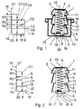
- the voltage converter shown in Figure 1 has a voltage divider 1, the carrier plate 2 and one on the carrier plate 2 by means of Thick film technology applied divider resistance 3 having.
- the divider resistor 3 is with taps 4, 5, 6, 7, 8, 9, and has a section on, which is designed as a measuring resistor 10.
- To the Voltage dividers 1 around are three umbrella-shaped Electrodes 11, 12, 13 arranged one below the other or capacitively effective with respect to the earth potential are.
- a first electrode 11 is connected to the High-voltage line 15 connected, which in turn on a first tap 4 of the divider resistor 3 connected.
- a second electrode 12 is included a second tap 5 of the divider resistor 3 connected via a short supply line 16.
- a third Electrode 13 is connected via a further short supply line 17 with a third tap 6 of the divider resistor 3 connected.
- the three electrodes 11, 12, 13 are stacked on top of each other.
- All taps 4 to 9 are on the edges of the Carrier plate 2 of the divider resistor 3 arranged to a simple connection to the high-voltage line 15, the short supply lines 16, 17 of the ground line 18 and to enable the measuring line 19.
- the electrodes are still in their dimensions matched to the desired capacity so that capacitive influences of the environment largely be neutralized.
- the electrodes 11, 12, 13 are shown in FIGS Examples designed as umbrella-shaped sheet metal parts, however, they can also be made using cast resin technology be, the capacitively effective part from a conductive synthetic resin layer or from a Spray metallization can exist.
- a High voltage U1 to the first tap 4 of the Divider resistor 3 created. Between the first Tap 4 and the second tap 5 becomes a first partial resistor R1 formed. Between the second tap 5 and the third tap 6 is a second partial resistor R2 is formed. Between the third tap 6 and the fourth tap 7 a third partial resistor R3 is formed. Between the fourth tap 7 and the fifth tap 8 the measuring resistor 10 is formed. After all, that is Earth line 18 connected to the sixth tap 9. The three electrodes 11, 12, 13 form one another the capacities C1, C2, C3. Parallel to Measuring resistor 10 is outside of the carrier plate 2 Compensation capacitor 20 to the fourth tap 7 and the fifth tap 8 connected. The Measuring voltage U2 is via the measuring line 19th decreased.
- a fourth cup-shaped electrode 14 arranged with is connected to earth potential and the third Whole electrode 13 and the second electrode 12 partially encloses.
- This fourth electrode 14 partially shields the voltage divider 1 and forms additional capacities C4 and C5 compared to the second Electrode 12 and third electrode 13.
- the fourth electrode and the three other electrodes 11, 12, 13 are something in their shape and arrangement modified so that in the associated Equivalent circuit only capacities C1 and C3 surrender.
- the voltage converter described is for voltages of about 12 kV (medium voltage) a division ratio of 1: 10000, so that the Measuring voltage is in the range of 1 V.
- FIG. 3 shows the voltage divider 1 again, the here from an overvoltage resistor 21 and an undervoltage resistor 22 exists between which a tap 23 is arranged.
- the measuring line 19 is connected to of the measuring voltage U2.
- the high voltage U1 is supplied via the high-voltage line 15.
- a support 31 for busbars poured.
- Such supports 31 are in Switchgear as an insulation part and for fastening and support of busbars used, the Supports 31 by means of a fastening screw 32 a bridge plate 33 are attached.
- the Fastening screw 32 is also a Earth connection to the tap 9 of the Divider resistor 3 ago.
- On the top of Support 31 becomes a bus bar, not shown by means of a fastening screw, not shown attached, while at the same time a contact to High-voltage line 15 is produced.
- a support 31 is again shown in FIGS. 6 and 7 shown with cast-in voltage converter, the but in this embodiment from the Divider resistor 3 and only one more Resistor 24 is formed, the two Carrier plates 2 at a short distance of about the thickness of a carrier plate substantially parallel to each other.
- the high voltage line 15 is via a connector 34 to both the first Tapping 4 of the divider resistor 3 as well as with the tapping the additional resistor 24 accordingly connected.
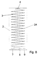
- a further resistor 24 In the voltage converter shown in Figure 8 on the front of the support plate 2 of the Divider resistor 3 and on the back of the same Carrier plate 2 arranged a further resistor 24.
- the further resistor 24 is connected to the first one Tap 4 of the divider resistor 3 connected to the the high voltage is applied. Even with the Tapping of the ground line Divider resistor 3 is in contact with the other End of further resistance 24.
- the fourth Tap 7 and the fifth tap 8, which for Tapping the measuring voltage serve, but are only with the divider resistor 3 connected.
Landscapes
- Physics & Mathematics (AREA)
- General Physics & Mathematics (AREA)
- Engineering & Computer Science (AREA)
- Power Engineering (AREA)
- Measuring Instrument Details And Bridges, And Automatic Balancing Devices (AREA)
- Fixed Capacitors And Capacitor Manufacturing Machines (AREA)
- Ac-Ac Conversion (AREA)
- Control Of Electrical Variables (AREA)
- Amplifiers (AREA)
Description
- Figur 1:
- eine erste schematische Ausführungsform des erfindungsgemäßen Spannungswandlers mit zugehörigem Ersatzschaltbild,
- Figur 2:
- eine zweite schematische Ausführungsform des erfindungsgemäßen Spannungswandlers mit zugehörigem Ersatzschaltbild,
- Figur 3:
- eine Prinzipskizze in perspektivischer Darstellung einer dritten Ausführungsform, eines erfindungsgemäßen Spannungswandlers,
- Figur 4:
- eine teilweise geschnittene Darstellung eines Ausführungsbeispiels der dritten Ausführungsform,
- Figur 5:
- einen Schnitt gemäß Linie A-A von Figur 4,
- Figur 6:
- eine teilweise geschnittene Darstellung eines weiteren Ausführungsbeispiels der dritten Ausführungsform,
- Figur 7:
- einen Schnitt gemäß Linie B-B von Figur 6,
- Figur 8:
- eine Draufsicht auf ein weiteres Ausführungsbeispiel der dritten Ausführungsform.
- 1
- Spannungsteiler
- 2
- Trägerplatte
- 3
- Teilerwiderstand
- 4
- erste Anzapfung
- 5
- zweite Anzapfung
- 6
- dritte Anzapfung
- 7
- vierte Anzapfung
- 8
- fünfte Anzapfung
- 9
- sechste Anzapfung
- 10
- Meßwiderstand
- 11
- erste Elektrode
- 12
- zweite Elektrode
- 13
- dritte Elektrode
- 14
- vierte Elektrode
- 15
- Hochspannunsleitung
- 16
- Zuleitung
- 17
- Zuleitung
- 18
- Erdleitung
- 19
- Meßleitung
- 20
- Kompensationskondensator
- 21
- Oberspannungswiderstand
- 22
- Unterspannungswiderstand
- 23
- Anzapfung
- 24
- weiterer Widerstand
- 25
- weiterer Widerstand
- 26
- weiterer Widerstand
- 27
- weiterer Widerstand
- 28
- Meßanschluß
- 29
- Verbinder
- 30
- Verbinder
- 31
- Stützer
- 32
- Befestigungsschraube
- 33
- Brückenplatte
- 34
- Verbinder
- U1
- Hochspannung
- U2
- Meßspannung
- R1
- erster Teilwiderstand
- R2
- zweiter Teilwiderstand
- R3
- dritter Teilwiderstand
- C1
- Kapazität
- C2
- Kapazität
- C3
- Kapazität
- C4
- Kapazität
- C5
- Kapazität
Claims (19)
- Spannungswandler mit Spannungsteiler (1) zur Spannungsmessung in Mittel- und Hochspannungsanlagen, mit einer kombinierten Anordnung von Ohmschem Teilerwiderstand (3) und Mitteln (11 bis 14, 24 bis 27) zur Kompensation von elektromagnetischen Umgebungseinflüssen, dadurch gekennzeichnet, daß ein Teilerwiderstand (3) einstückig mit einem Meßwiderstand (10) und mit Anzapfungen (4 bis 9) als auf eine Trägerplatte (2) aufgedampfter Metallwerkstoff oder in Dickschichttechnik ausgeführt ist, wobei die Anzapfungen (4 bis 9) an den Rändern der Trägerplatte (2) angeordnet sind und mindestens eine Anzapfung (4 bis 9) mit mindestens einem Kompensationselement (11 bis 14, 24 bis 27) verbunden ist.
- Spannungswandler nach Anspruch 1, dadurch gekennzeichnet, daß als Kompensationselemente Elektroden (11, 12, 13) verwendet werden, die derart dimensioniert sind, daß zufällige und von der Umgebung herrührende kapazitive Einflüsse weitgehend kompensiert werden, insbesondere dadurch, daß die Kapazität am Unterspannungswiderstand (22) in einem bestimmten Verhältnis zur Kapazität am Oberspannungswiderstand (21) steht.
- Spannungswandler nach Anspruch 2, dadurch gekennzeichnet, daß die Elektroden in Gießharztechnik ausgeführt sind, wobei der kapazitiv wirksame Teil aus leitfähigen Kunstharzschichten oder Spritzmetallisierung besteht.
- Spannungswandler nach Anspruch 2, dadurch gekennzeichnet, daß die kapazitiven Elektroden (11, 12, 13) aus geeignet geformten Blechteilen bestehen, die über kurze Zuleitungen (16, 17) mit den Anzapfungen (4, 5, 6) des Teilerwiderstands (3) verbunden sind.
- Spannungswandler nach Anspruch 2, dadurch gekennzeichnet, daß die kapazitiven Elektroden (11, 12, 13) aus schirmförmigen Metallteilen bestehen.
- Spannungswandler nach Anspruch 2, dadurch gekennzeichnet, daß die Elektroden halbleitfähig ausgestaltet sind, vorzugsweise mit einem Oberflächenwiderstand im Bereich von 108...1011 Ω.
- Spannungswandler nach Anspruch 4, 5 oder 6, dadurch gekennzeichnet, daß drei schirmförmige Elektroden (11, 12, 13) übereinander angeordnet sind, wobei eine erste Elektrode (11) mit der Hochspannung (U1), eine zweite Elektrode (12) mit einer zweiten Anzapfung (5) des Teilerwiderstands (3) und eine dritte Elektrode (13) mit einer dritten Anzapfung (6) verbunden ist.
- Spannungswandler nach Anspruch 7, dadurch gekennzeichnet, daß eine topfförmige, mit dem Erdpotential verbundene vierte Elektrode (14) vorgesehen ist, die zumindest die dritte Elektrode (13) umschließt.
- Spannungswandler nach Anspruch 7, dadurch gekennzeichnet, daß eine topfförmige, mit dem Potential des Teilerabgriffes an der vierten Anzapfung (7) verbundene vierte Elektrode (14) vorgesehen ist, die zumindest einen Teil des Teilerwiderstandes umschließt.
- Spannungswandler nach Anspruch 1, dadurch gekennzeichnet, daß als Kompensationselement mindestens ein weiterer Widerstand (24, 25, 26, 27) parallel zum Teilerwiderstand (3) geschaltet und in dessen Nähe angeordnet ist.
- Spannungswandler nach Anspruch 10, dadurch gekennzeichnet, daß der oder die weiteren Widerstände (24, 25, 26, 27) als auf ein Trägermaterial (2) aufgedampfter Metallwerkstoff oder in Dickschichttechnik ausgeführt ist sind.
- Spannungswandler nach Anspruch 10 oder 11, dadurch gekennzeichnet, daß der oder die weiteren Widerstände (24, 25, 26, 27) in gleicher Bauart wie der Teilerwiderstand (3) auf einer ebenen Trägerplatte (2) mit Anzapfungen (4, 7, 8, 9) an den Rändern der Trägerplatte (2) ausgeführt ist sind, wobei aber nur der Teilerwiderstand (3) mit dem Meßanschluß (28) verbunden ist.
- Spannungswandler nach Anspruch 12, dadurch gekennzeichet, daß vier weitere Widerstände (24, 25, 26, 27) kastenförmig um den Teilerwiderstand (3) herum angeordnet sind, so daß ihre Trägerplatten (2) im Schnitt im wesentlichen ein Quadrat bilden, in dem der Teilerwiderstand (3) diagonal angeordnet ist.
- Spannungswandler nach Anspruch 12, dadurch gekennzeichnet, daß ein weiterer Widerstand (24) direkt neben dem Teilerwiderstand (3) angeordnet ist, so daß die beiden Trägerplatten (2) in einem geringen Abstand im wesentlichen parallel zueinander verlaufen.
- Spannungswandler nach Anspruch 12, dadurch gekennzeichnet, daß der Teilerwiderstand (3) und ein weiterer Widerstand (24) auf Vorder- und Rückseite derselben Trägerplatte (2) angeordnet sind.
- Spannungswandler nach einem der Ansprüche 1 bis 15, dadurch gekennzeichnet, daß der Spannungswandler in das Material eines Isolationsteiles einer Schaltanlage, insbesondere in eine Durchführung oder einen Stützer (31) für Stromschienen eingegossen ist.
- Spannungswandler nach Anspruch 16, dadurch gekennzeichnet, daß die Widerstände (24, 25, 26, 27) des Spannungswandlers und insbesondere der Teilerwiderstand (3) mit Silikonkautschuk überzogen sind.
- Stützer für Stromschienen, Insbesondere von Schaltanlagen, dadurch gekennzeichnet, daß in das Material des Stützers (31) ein Spannungswandler gemäß einem der Ansprüche 1 bis 15 eingegossen ist.
- Stützer nach Anspruch 18, dadurch gekennzeichnet, daß die Widerstände (24, 25, 26, 27) des Spannungswandlers und insbesondere der Teilerwiderstand (3) mit Silikonkautschuk überzogen sind.
Applications Claiming Priority (3)
| Application Number | Priority Date | Filing Date | Title |
|---|---|---|---|
| DE19508582A DE19508582A1 (de) | 1995-03-13 | 1995-03-13 | Spannungswandler |
| DE19508582 | 1995-03-13 | ||
| PCT/EP1995/004431 WO1996028736A1 (de) | 1995-03-13 | 1995-11-10 | Spannungswandler |
Publications (2)
| Publication Number | Publication Date |
|---|---|
| EP0815454A1 EP0815454A1 (de) | 1998-01-07 |
| EP0815454B1 true EP0815454B1 (de) | 1999-01-27 |
Family
ID=7756266
Family Applications (1)
| Application Number | Title | Priority Date | Filing Date |
|---|---|---|---|
| EP95939257A Expired - Lifetime EP0815454B1 (de) | 1995-03-13 | 1995-11-10 | Spannungswandler |
Country Status (5)
| Country | Link |
|---|---|
| US (1) | US5883508A (de) |
| EP (1) | EP0815454B1 (de) |
| AT (1) | ATE176332T1 (de) |
| DE (2) | DE19508582A1 (de) |
| WO (1) | WO1996028736A1 (de) |
Cited By (1)
| Publication number | Priority date | Publication date | Assignee | Title |
|---|---|---|---|---|
| WO2006039976A1 (de) * | 2004-10-16 | 2006-04-20 | Duromer Kunststoffverarbeitungs- Gmbh | Spannungsteiler |
Families Citing this family (20)
| Publication number | Priority date | Publication date | Assignee | Title |
|---|---|---|---|---|
| DE19703300C1 (de) * | 1997-01-30 | 1998-05-14 | Ritz Messwandler Kg | Spannungsteiler für Mittelspannungsanlagen |
| DE19719521A1 (de) * | 1997-05-09 | 1998-11-19 | Felten & Guilleaume Energie | Spannungssensor für Meß- und Schutzwerke für Mittelspannungsschaltanlagen |
| DE59801018D1 (de) * | 1997-09-16 | 2001-08-16 | Trench Switzerland Ag Basel | Spannungsteiler |
| EP0980003B1 (de) * | 1998-08-12 | 2006-03-08 | Trench Switzerland AG | RC-Spannungsteiler |
| DE19841164A1 (de) * | 1998-09-09 | 2000-03-16 | Abb Research Ltd | Spannungsteileranordnung |
| US7123032B2 (en) * | 2003-12-04 | 2006-10-17 | Fieldmetrics, Inc. | Voltage sensor and dielectric material |
| US7129693B2 (en) * | 2004-07-19 | 2006-10-31 | Fieldmetrics, Inc. | Modular voltage sensor |
| US7902907B2 (en) * | 2007-12-12 | 2011-03-08 | Micron Technology, Inc. | Compensation capacitor network for divided diffused resistors for a voltage divider |
| CN101901681B (zh) * | 2009-05-26 | 2012-04-25 | 廊坊高山电子科技有限公司 | 一种10kv无源电子式电压互感器 |
| FR2958755B1 (fr) * | 2010-04-13 | 2012-09-21 | Schneider Electric Ind Sas | Dispositif de mesure a diviseur de tension electrique. |
| WO2013041649A1 (de) | 2011-09-23 | 2013-03-28 | Basf Se | Verwendung einer wässrigen dispersion biologisch abbaubarer polyester |
| ES2586827T3 (es) * | 2011-12-31 | 2016-10-19 | Siemens Aktiengesellschaft | Transformador combinado para sistema de energía |
| CN103187162B (zh) * | 2011-12-31 | 2016-08-17 | 上海Mwb互感器有限公司 | 用于电力系统的组合互感器 |
| EP2696206B1 (de) | 2012-08-06 | 2023-11-01 | ABB Schweiz AG | Mittel- oder Hochspannungsanordnung mit Kabelverbindungsendgerät |
| FR2998376B1 (fr) * | 2012-11-16 | 2015-07-31 | Alstom Technology Ltd | Capteur de tension de ligne a tres haute tension a courant continu |
| CN104459262A (zh) * | 2014-12-04 | 2015-03-25 | 中国西电电气股份有限公司 | 一种高压测量电阻分压器 |
| US10613243B2 (en) * | 2017-04-27 | 2020-04-07 | Franklin Sensors Inc. | Apparatus and methods for obscured feature detection |
| CN108957095B (zh) * | 2018-06-13 | 2024-07-02 | 贵州电网有限责任公司 | 一种直流电压互感器及其电压测试方法 |
| US11125782B2 (en) | 2018-12-07 | 2021-09-21 | Abb Schweiz Ag | Line post sensor |
| GB2579838B (en) * | 2018-12-17 | 2021-09-29 | Ge Aviat Systems Ltd | Method and circuit for detecting an arc fault |
Family Cites Families (13)
| Publication number | Priority date | Publication date | Assignee | Title |
|---|---|---|---|---|
| DE1516244A1 (de) * | 1965-03-11 | 1969-05-22 | Siemens Ag | Ohmscher Spannungsteiler fuer hohe Spannungen und Frequenzen |
| DE2027735B2 (de) * | 1969-09-19 | 1972-06-29 | VEB Transformatoren- und Röntgenwerk Dresden, χ 8030 Dresden | Messpannungsverteiler fuer eine sehr hohe, mit einer wechselspannung ueberlagerte gleichspannung |
| DD100810A1 (de) * | 1972-12-13 | 1973-10-05 | ||
| DE2930672C2 (de) * | 1979-07-28 | 1985-02-07 | Brown, Boveri & Cie Ag, 6800 Mannheim | Spannungsteiler zur Messung hoher Wechselspannungen in Hochspannungsschaltanlagen |
| FR2462713A1 (fr) * | 1979-07-28 | 1981-02-13 | Bbc Brown Boveri & Cie | Dispositif de mesure de tensions continues elevees |
| DE2930767A1 (de) * | 1979-07-28 | 1981-02-19 | Bbc Brown Boveri & Cie | Einrichtung zur messung hoher gleichspannungen |
| DE3304316A1 (de) * | 1983-02-09 | 1984-08-09 | Philips Patentverwaltung Gmbh, 2000 Hamburg | Mess- und daempfungswiderstandsanordnung fuer ein hochspannungsgeraet |
| DE8323693U1 (de) * | 1983-08-17 | 1986-05-07 | Siemens AG, 1000 Berlin und 8000 München | Stützisolator für Hochspannung |
| DE3445898A1 (de) * | 1984-12-15 | 1986-06-19 | Licentia Patent-Verwaltungs-Gmbh, 6000 Frankfurt | Verfahren zur kompensation von stoerkapazitaeten zwischen einem widerstand und einer elektrisch leitenden abschirmelektrode |
| DE3714945A1 (de) * | 1986-05-09 | 1987-11-12 | Koch & Sterzel Kg | Frequenzunabhaengiger kapazitiv-ohmscher spannungsteiler zum messen von hochspannungen in mittel- und hochfrequenten roentgengeneratoren |
| JPH0821481B2 (ja) * | 1988-11-30 | 1996-03-04 | 大陽誘電株式会社 | 膜状抵抗体及びそのトリミング方法 |
| US5241260A (en) * | 1989-12-07 | 1993-08-31 | Electromed International | High voltage power supply and regulator circuit for an X-ray tube with transient voltage protection |
| US5220495A (en) * | 1991-09-18 | 1993-06-15 | S&C Electric Company | Arrangement and method for accurately sensing voltage of a high-impedance source and supplying power to a variable burden |
-
1995
- 1995-03-13 DE DE19508582A patent/DE19508582A1/de not_active Withdrawn
- 1995-11-10 DE DE59505011T patent/DE59505011D1/de not_active Expired - Fee Related
- 1995-11-10 US US08/913,922 patent/US5883508A/en not_active Expired - Fee Related
- 1995-11-10 AT AT95939257T patent/ATE176332T1/de not_active IP Right Cessation
- 1995-11-10 EP EP95939257A patent/EP0815454B1/de not_active Expired - Lifetime
- 1995-11-10 WO PCT/EP1995/004431 patent/WO1996028736A1/de not_active Ceased
Cited By (1)
| Publication number | Priority date | Publication date | Assignee | Title |
|---|---|---|---|---|
| WO2006039976A1 (de) * | 2004-10-16 | 2006-04-20 | Duromer Kunststoffverarbeitungs- Gmbh | Spannungsteiler |
Also Published As
| Publication number | Publication date |
|---|---|
| DE19508582A1 (de) | 1996-09-26 |
| EP0815454A1 (de) | 1998-01-07 |
| DE59505011D1 (de) | 1999-03-11 |
| US5883508A (en) | 1999-03-16 |
| ATE176332T1 (de) | 1999-02-15 |
| WO1996028736A1 (de) | 1996-09-19 |
Similar Documents
| Publication | Publication Date | Title |
|---|---|---|
| EP0815454A1 (de) | Spannungswandler | |
| EP1566868B1 (de) | Überspannungsschutzelement und Zündelement für ein Überspannungsschutzelement | |
| DE69923194T2 (de) | Leitfähiger kontakt | |
| DE69633848T2 (de) | Leiterplattenfunkenstrecke | |
| DE69414548T2 (de) | Eine Vorrichtung, die einen Verteilerkasten (Zentralelektrik) bildet, mit einem eingesetzten Shuntwiderstand | |
| EP0637099B1 (de) | Reihenklemmenanordnung mit Überspannungsschutzorganen | |
| CH670004A5 (de) | ||
| DE2501247B2 (de) | Zündverteiler für Verbrennungsmotoren mit einer Entstöreinrichtung | |
| DE3600447A1 (de) | Entkopplungskondensator und verfahren zu seiner herstellung | |
| EP0980003B1 (de) | RC-Spannungsteiler | |
| EP0152127A2 (de) | Anordnung zum Unterdrücken von Überspannungsspitzen | |
| DE4414529A1 (de) | Drehwinkelsensor vom Kapazitätstyp | |
| DE69306507T2 (de) | Hochfrequenzschaltung und Verfahren zur deren Herstellung | |
| DE1463269A1 (de) | Vorionisator fuer UEberspannungsschutzeinrichtungen | |
| DE102007042358B3 (de) | Elektrische Schutzvorrichtung | |
| DE3907199C3 (de) | Überspannungsschutzgerät für Koaxialkabel | |
| DE2752690A1 (de) | Ionisations-brandmelder | |
| DE10125941B4 (de) | Kompaktanordnung für mehrpolige stoßstromfeste Überspannungsableiter | |
| DE69827935T2 (de) | Antennenelement | |
| EP0635919A2 (de) | Überspannungsschutzelement | |
| DE3702780A1 (de) | Integrierte Varistor-Schutzvorrichtung zum Schutz eines Elektronikbauteils gegen die Wirkungen von elektromagnetischen Feldern oder statischen Ladungen | |
| AT521667B1 (de) | Spannungsteilungsvorrichtung mit Siloxan-Dielektrikum | |
| DE102014109990B4 (de) | Messwiderstand mit vertikalem Stromfluss, Halbleiterpackage mit einem Messwiderstand und Verfahren zur Herstellung eines Messwiderstandes | |
| DE102016218478B4 (de) | Symmetrischer Spannungsteiler | |
| DE2700388C2 (de) | Entstöranordnung an einem Elektrowerkzeug oder -gerät mit einem ganz oder teilweise aus Metall bestehenden Gehäuse |
Legal Events
| Date | Code | Title | Description |
|---|---|---|---|
| PUAI | Public reference made under article 153(3) epc to a published international application that has entered the european phase |
Free format text: ORIGINAL CODE: 0009012 |
|
| 17P | Request for examination filed |
Effective date: 19970712 |
|
| AK | Designated contracting states |
Kind code of ref document: A1 Designated state(s): AT BE CH DE FR GB IT LI |
|
| RBV | Designated contracting states (corrected) |
Designated state(s): AT BE CH DE FR GB IT LI |
|
| GRAG | Despatch of communication of intention to grant |
Free format text: ORIGINAL CODE: EPIDOS AGRA |
|
| GRAG | Despatch of communication of intention to grant |
Free format text: ORIGINAL CODE: EPIDOS AGRA |
|
| GRAH | Despatch of communication of intention to grant a patent |
Free format text: ORIGINAL CODE: EPIDOS IGRA |
|
| 17Q | First examination report despatched |
Effective date: 19980421 |
|
| GRAH | Despatch of communication of intention to grant a patent |
Free format text: ORIGINAL CODE: EPIDOS IGRA |
|
| GRAA | (expected) grant |
Free format text: ORIGINAL CODE: 0009210 |
|
| AK | Designated contracting states |
Kind code of ref document: B1 Designated state(s): AT BE CH DE FR GB IT LI |
|
| REF | Corresponds to: |
Ref document number: 176332 Country of ref document: AT Date of ref document: 19990215 Kind code of ref document: T |
|
| REG | Reference to a national code |
Ref country code: CH Ref legal event code: EP |
|
| REG | Reference to a national code |
Ref country code: CH Ref legal event code: NV Representative=s name: PATENTANWALTSBUERO RENFER-VONNEMANN |
|
| GBT | Gb: translation of ep patent filed (gb section 77(6)(a)/1977) |
Effective date: 19990202 |
|
| REF | Corresponds to: |
Ref document number: 59505011 Country of ref document: DE Date of ref document: 19990311 |
|
| ET | Fr: translation filed | ||
| PLBE | No opposition filed within time limit |
Free format text: ORIGINAL CODE: 0009261 |
|
| STAA | Information on the status of an ep patent application or granted ep patent |
Free format text: STATUS: NO OPPOSITION FILED WITHIN TIME LIMIT |
|
| 26N | No opposition filed | ||
| REG | Reference to a national code |
Ref country code: GB Ref legal event code: IF02 |
|
| REG | Reference to a national code |
Ref country code: CH Ref legal event code: PCAR Free format text: DUROMER KUNSTSTOFFVERARBEITUNGS-GMBH#BERGENER RING 65-67#01458 OTTENDORF-OKRILLA (DE) -TRANSFER TO- DUROMER KUNSTSTOFFVERARBEITUNGS-GMBH#BERGENER RING 65-67#01458 OTTENDORF-OKRILLA (DE) Representative=s name: PATENTANWALTSBUERO URSULA RENFER-VONNEMANN, CH |
|
| PGFP | Annual fee paid to national office [announced via postgrant information from national office to epo] |
Ref country code: GB Payment date: 20051026 Year of fee payment: 11 |
|
| PGFP | Annual fee paid to national office [announced via postgrant information from national office to epo] |
Ref country code: FR Payment date: 20051118 Year of fee payment: 11 |
|
| PGFP | Annual fee paid to national office [announced via postgrant information from national office to epo] |
Ref country code: AT Payment date: 20051122 Year of fee payment: 11 |
|
| PGFP | Annual fee paid to national office [announced via postgrant information from national office to epo] |
Ref country code: BE Payment date: 20051123 Year of fee payment: 11 |
|
| PGFP | Annual fee paid to national office [announced via postgrant information from national office to epo] |
Ref country code: DE Payment date: 20060126 Year of fee payment: 11 |
|
| PGFP | Annual fee paid to national office [announced via postgrant information from national office to epo] |
Ref country code: CH Payment date: 20060206 Year of fee payment: 11 |
|
| PG25 | Lapsed in a contracting state [announced via postgrant information from national office to epo] |
Ref country code: AT Free format text: LAPSE BECAUSE OF NON-PAYMENT OF DUE FEES Effective date: 20061110 |
|
| PG25 | Lapsed in a contracting state [announced via postgrant information from national office to epo] |
Ref country code: LI Free format text: LAPSE BECAUSE OF NON-PAYMENT OF DUE FEES Effective date: 20061130 Ref country code: CH Free format text: LAPSE BECAUSE OF NON-PAYMENT OF DUE FEES Effective date: 20061130 Ref country code: BE Free format text: LAPSE BECAUSE OF NON-PAYMENT OF DUE FEES Effective date: 20061130 |
|
| PGFP | Annual fee paid to national office [announced via postgrant information from national office to epo] |
Ref country code: IT Payment date: 20061130 Year of fee payment: 12 |
|
| PG25 | Lapsed in a contracting state [announced via postgrant information from national office to epo] |
Ref country code: DE Free format text: LAPSE BECAUSE OF NON-PAYMENT OF DUE FEES Effective date: 20070601 |
|
| REG | Reference to a national code |
Ref country code: CH Ref legal event code: PL |
|
| GBPC | Gb: european patent ceased through non-payment of renewal fee |
Effective date: 20061110 |
|
| REG | Reference to a national code |
Ref country code: FR Ref legal event code: ST Effective date: 20070731 |
|
| PG25 | Lapsed in a contracting state [announced via postgrant information from national office to epo] |
Ref country code: GB Free format text: LAPSE BECAUSE OF NON-PAYMENT OF DUE FEES Effective date: 20061110 |
|
| BERE | Be: lapsed |
Owner name: *DUROMER KUNSTSTOFFVERARBEITUNGS-G.M.B.H. Effective date: 20061130 |
|
| PG25 | Lapsed in a contracting state [announced via postgrant information from national office to epo] |
Ref country code: FR Free format text: LAPSE BECAUSE OF NON-PAYMENT OF DUE FEES Effective date: 20061130 |
|
| PG25 | Lapsed in a contracting state [announced via postgrant information from national office to epo] |
Ref country code: IT Free format text: LAPSE BECAUSE OF NON-PAYMENT OF DUE FEES Effective date: 20071110 |