EP0814423A2 - Methods and apparatus for data entry - Google Patents
Methods and apparatus for data entry Download PDFInfo
- Publication number
- EP0814423A2 EP0814423A2 EP97202375A EP97202375A EP0814423A2 EP 0814423 A2 EP0814423 A2 EP 0814423A2 EP 97202375 A EP97202375 A EP 97202375A EP 97202375 A EP97202375 A EP 97202375A EP 0814423 A2 EP0814423 A2 EP 0814423A2
- Authority
- EP
- European Patent Office
- Prior art keywords
- electrode
- strips
- electrode strips
- pad
- measuring
- Prior art date
- Legal status (The legal status is an assumption and is not a legal conclusion. Google has not performed a legal analysis and makes no representation as to the accuracy of the status listed.)
- Granted
Links
Images


Classifications
-
- G—PHYSICS
- G06—COMPUTING; CALCULATING OR COUNTING
- G06F—ELECTRIC DIGITAL DATA PROCESSING
- G06F3/00—Input arrangements for transferring data to be processed into a form capable of being handled by the computer; Output arrangements for transferring data from processing unit to output unit, e.g. interface arrangements
- G06F3/01—Input arrangements or combined input and output arrangements for interaction between user and computer
- G06F3/02—Input arrangements using manually operated switches, e.g. using keyboards or dials
- G06F3/0202—Constructional details or processes of manufacture of the input device
- G06F3/021—Arrangements integrating additional peripherals in a keyboard, e.g. card or barcode reader, optical scanner
- G06F3/0213—Arrangements providing an integrated pointing device in a keyboard, e.g. trackball, mini-joystick
-
- G—PHYSICS
- G06—COMPUTING; CALCULATING OR COUNTING
- G06F—ELECTRIC DIGITAL DATA PROCESSING
- G06F3/00—Input arrangements for transferring data to be processed into a form capable of being handled by the computer; Output arrangements for transferring data from processing unit to output unit, e.g. interface arrangements
- G06F3/01—Input arrangements or combined input and output arrangements for interaction between user and computer
- G06F3/03—Arrangements for converting the position or the displacement of a member into a coded form
- G06F3/033—Pointing devices displaced or positioned by the user, e.g. mice, trackballs, pens or joysticks; Accessories therefor
- G06F3/0354—Pointing devices displaced or positioned by the user, e.g. mice, trackballs, pens or joysticks; Accessories therefor with detection of 2D relative movements between the device, or an operating part thereof, and a plane or surface, e.g. 2D mice, trackballs, pens or pucks
- G06F3/03547—Touch pads, in which fingers can move on a surface
-
- G—PHYSICS
- G06—COMPUTING; CALCULATING OR COUNTING
- G06F—ELECTRIC DIGITAL DATA PROCESSING
- G06F3/00—Input arrangements for transferring data to be processed into a form capable of being handled by the computer; Output arrangements for transferring data from processing unit to output unit, e.g. interface arrangements
- G06F3/01—Input arrangements or combined input and output arrangements for interaction between user and computer
- G06F3/03—Arrangements for converting the position or the displacement of a member into a coded form
- G06F3/041—Digitisers, e.g. for touch screens or touch pads, characterised by the transducing means
- G06F3/0416—Control or interface arrangements specially adapted for digitisers
- G06F3/04166—Details of scanning methods, e.g. sampling time, grouping of sub areas or time sharing with display driving
-
- G—PHYSICS
- G06—COMPUTING; CALCULATING OR COUNTING
- G06F—ELECTRIC DIGITAL DATA PROCESSING
- G06F3/00—Input arrangements for transferring data to be processed into a form capable of being handled by the computer; Output arrangements for transferring data from processing unit to output unit, e.g. interface arrangements
- G06F3/01—Input arrangements or combined input and output arrangements for interaction between user and computer
- G06F3/03—Arrangements for converting the position or the displacement of a member into a coded form
- G06F3/041—Digitisers, e.g. for touch screens or touch pads, characterised by the transducing means
- G06F3/044—Digitisers, e.g. for touch screens or touch pads, characterised by the transducing means by capacitive means
- G06F3/0445—Digitisers, e.g. for touch screens or touch pads, characterised by the transducing means by capacitive means using two or more layers of sensing electrodes, e.g. using two layers of electrodes separated by a dielectric layer
-
- G—PHYSICS
- G06—COMPUTING; CALCULATING OR COUNTING
- G06F—ELECTRIC DIGITAL DATA PROCESSING
- G06F3/00—Input arrangements for transferring data to be processed into a form capable of being handled by the computer; Output arrangements for transferring data from processing unit to output unit, e.g. interface arrangements
- G06F3/01—Input arrangements or combined input and output arrangements for interaction between user and computer
- G06F3/03—Arrangements for converting the position or the displacement of a member into a coded form
- G06F3/041—Digitisers, e.g. for touch screens or touch pads, characterised by the transducing means
- G06F3/044—Digitisers, e.g. for touch screens or touch pads, characterised by the transducing means by capacitive means
- G06F3/0446—Digitisers, e.g. for touch screens or touch pads, characterised by the transducing means by capacitive means using a grid-like structure of electrodes in at least two directions, e.g. using row and column electrodes
-
- G—PHYSICS
- G06—COMPUTING; CALCULATING OR COUNTING
- G06F—ELECTRIC DIGITAL DATA PROCESSING
- G06F2203/00—Indexing scheme relating to G06F3/00 - G06F3/048
- G06F2203/033—Indexing scheme relating to G06F3/033
- G06F2203/0333—Ergonomic shaped mouse for one hand
Definitions
- This invention relates generally to methods and apparatus for data input. More specifically, this invention relates to touch sensitive input devices for data input to computers and other instruments.
- Input devices for computers are well known in the art. There are several types of input devices, such as the familiar "mouse”, which have been utilized and are generally useful in providing "user friendly” computer systems for both technical and non-technical applications. The popularity which these devices have achieved in the art can be given large credit for fostering the explosive growth of the personal computer industry since they provide a simple means for users to input data to computers for users.
- mice generally require a free-rolling surface on which it can interface. Depending upon the particular mouse which is used, the device couples to the free-rolling surface and translates movement across the surface as an input to a computer. Thus, the mouse is unsuitable for any input application which cannot provide space for a rolling surface.
- the current and growing popularity of "laptop" computers thus has created a significant problem for mouse type technologies which require a rolling surface. Laptops are generally used in small confined areas such as, for example, airplanes, where there is insufficient room for a rolling surface. Therefore, a long-felt need in the art exists for non-mouse pointing solutions for computers and other instruments.
- U.S. Patent No. 3,886,311 discloses a writing pen for detecting time varying electrostatic field components.
- the writing pen disclosed in Rodgers et al. is used in conjunction with a writing tablet which generates an electrostatic field.
- the Rodgers et al. patent discloses an X-Y grid having a writing surface overlaying the grid and an active stylus which writes on the grid in the same manner as a ball point pen. See column 2, lines 63, through column 3, line 7.
- Other examples of stylus-type or "tablet" input devices are disclosed in U.S. Patent No. 4,672,154, also to Rodgers et al. The second Rodgers et al.
- the Rodgers et al. patents disclose digitizing styluses and mouse pointing devices which require a separate rolling surface. Furthermore, both of these patents disclose devices which are active and emit electrostatic fields to interact with the digitizing tablet in order to input data to a computer. Since the devices disclosed in both Rodgers et al. patents are active, the stylus is either attached to the tablet by a wire or contains a replaceable power source such as a battery. In either case, the user is required to grasp a bulky item in order to use the device. Thus, the devices disclosed in the Rodgers et al. patents do not satisfy a long-felt need in the art for pointing and input devices which can be conveniently and efficiently used for a variety of portable and desktop applications.
- Yoshikawa et al. discloses a coordinate detecting apparatus for determining the coordinate position data of a point on a plane indicated by the touch of a finger tip or other load.
- Yoshikawa et al. teaches an analog type apparatus which uses a resistive film through which the coordinate position of a point is detected. The point's coordinate position is indicated by applying a load impedance to the position. See column 3, lines 8 through 22.
- Tactile devices such as those disclosed in Yoshikawa et al. exhibit a significant disadvantage since they require electrical contact between the finger tip and the device. When individuals possess long fingernails or have other objects about the fingers and hands, good electrical contact is prevented and the device does not function properly.
- U.S. Patent No. 4,736,191, Matzke discloses a touch activated control device comprising individual conductive plates which form sectors of a circle. A user's touch on the dielectric layer overlaying the plates is detected by individually charging and discharging each of the sectors in the plates in a sequential manner to determine the increased capacitance of the sector. See column 2, lines 26 through 40.
- Ng et al. discloses a display device which locates a touch anywhere on a conductive display faceplate by measuring plural electrical impedances of the faceplate's conductive coating. The impedances are at electrodes located on different edges of the faceplate. See column 2, lines 7 through 12.
- the touch-sensitive devices disclosed in Ng et al. are generally designed to overlay a computer display and provide positioning information.
- the tactile input devices disclosed in the Bobick, Matzke et al. and Ng et al. patents do not satisfy a long-felt need in the art for tactile input devices which accurately and efficiently provide data input for computers and other instrumentation.
- the devices disclosed in the aforementioned patents fail to satisfy this long-felt need since they effectively only measure position as a fraction of the distance between electrodes located on the boundaries of a sensing region. This leads to measurement inaccuracies since the distance between electrodes is relatively large, thereby causing small errors in the measured fraction to result in large position errors.
- Still other tactile sensing devices utilize a grid of electrodes to digitally determine an object's position somewhere on the grid. See U.S. Patent No. 4,550,221, Mabusth, and U.S. Patent No. 4,639,720, Rympalski et al.
- the Mabusth patent discloses a touch sensitive control device which translates touch location to output signals and which includes a substrate that supports first and second interleaved, closely spaced, non-overlapping conducting plates. The plates are aligned in rows and columns so that edges of each plate of an array are proximate to, but spaced apart from, the edges of plates of the other array.
- the first and second arrays are periodically connected in a multiplexed fashion to a capacitance measuring circuit which measures the change in capacitance in the arrays.
- the Mabusth patent discloses a grid of pixels which are capacitively coupled.
- the Rympalski et al. patent discloses an electronic sketch pad which contains a graphics input pad having an array of transparent capacitive pixels, the capacitance characteristics of which are changed in response to the passing of a conductive tipped stylus over the surface of the pad.
- the change in capacitance is sensed by buffers disposed along the columns of the pixel matrix as the rows are scanned at a prescribed scanning rate.
- An apparatus for data input comprises pad means for sensing at least one object's position, the pad means having electrical balances responsive to the object's position, and measurement means operatively coupled to the pad means for measuring the electrical balances in the pad means.
- the methods comprise the steps of providing an electrically sensitive pad comprising insulator means having first and second sides for providing an insulating substrate to the apparatus, first electrode means electrically coupled to the first side of the insulator means for establishing an electromagnetic field, second electrode means electrically coupled to the second side of the insulator means for further establishing the electromagnetic field in cooperation with the first electrode means, synthesis means operatively coupled to the first electrode means and the second electrode means for selecting first electrode means and second electrode means to repeatedly synthesize virtual dipole electrodes.
- the steps of the methods further comprise measuring electrical balances between the plurality of first electrode means and the second electrode means, calculating the object's coarse position based on a least one target index, calculating the object's fine position based on the measured balances between the plurality of first electrode and second electrode means, and calculating the object's net position.
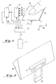
- FIG. 1 is a block diagram of a touch sensitive control device provided in accordance with this invention.
- Figure 2 shows a touch sensitive control device provided in accordance with this invention interfaced with a computer keyboard.
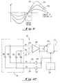
- Figure 3 illustrates synthesis of virtual electrodes.
- Figure 4 shows synthesis of virtual dipole electrodes from virtual electrodes.
- Figure 5(a) illustrates a simple virtual dipole electrode.
- Figure 5(b) illustrates a simple virtual dipole electrode wrapped around.
- Figure 6 illustrates cyclic virtual dipole electrodes.
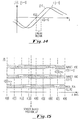
- Figure 7 is a block diagram of a virtual electrode pad and row and column synthesis circuitry.
- Figure 8(a) shows an elevation view of a virtual electrode pad provided in accordance with this invention.
- Figure 8(b) is a plan view of a virtual electrode pad taken along the 8(b) line of Figure 8(a).
- Figure 9 is a block diagram of row and column synthesis circuitry.
- Figure 10(a) illustrates object position sensing with a touch sensitive control device provided in accordance with this invention.
- Figure 10(b) shows object position sensing taken along the 10(b) line of Figure 10(a).
- Figure 11 is a graph of electrical balance versus position for a sensed object.
- Figure 12 illustrates a preferred embodiment of the electrical balance measurement circuit of Figure 1.
- Figure 13 is a virtual dipole electrode pad on which a single row virtual dipole electrode and two column virtual dipole electrodes are synthesized.
- Figure 14 is a graph of balances versus object position for the arrangement of Figure 13.
- Figure 15 shows target and base virtual dipole electrode extent with indices updated reflecting sensed object position.
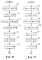
- Figure 16 is a preferred embodiment of a flow chart of a control algorithm provided in accordance with this invention.
- Figure 17 is a flow chart to determine the proximity of an object to a virtual dipole electrode pad.
- Figure 18 is a flow chart to determine the x position of an object.
- Figure 19 is a flow chart to determine the y position of an object.
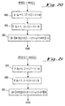
- Figure 20 is a flow chart to accomplish x position index updating.
- Figure 21 is a flow chart to accomplish y position index updating.
- Figure 1 is a touch sensitive input device provided in accordance with this invention, comprised of a virtual electrode pad 20, electrical balance measurement circuit 30, balance ratio determination circuit 40, and control circuit 50.
- virtual electrode pad 20 is in the shape of a sheet.
- the virtual electrode pad 20 is capable of forming "virtual electrodes" at various positions on its top and bottom surfaces. The electrodes are denoted as “virtual electrodes” since separate conductive strips on the two sides of pad 20 are used to form single elements denoted “virtual electrodes.”
- the virtual electrodes are connected to electronic circuitry capable of measuring the electrical balance between selected top virtual electrodes and selected bottom virtual electrodes.
- balance ratio determination circuit 40 is provided to determine the ratio of one balance measurement to another.
- Control circuit 50 selects appropriate electrodes for balance measurement and ratio determination.
- the control circuit 50 responds to balance ratios to calculate position information of the sensed object 60. This information may include position along 1 or 2 axes parallel to the electrode pad surface. Additional "proximity" information along an axis perpendicular to the surface of electrode pad 20 may also be determined from an appropriate balance measurement.
- Position information determined by control circuit 50 is provided to a utilization means 70 which may be any of a variety of electronic or computer devices.
- a finger 60 is shown located with its tip in close proximity to the top surface of electrode pad 20.
- the position of the finger tip over some region in the x and y directions may be sensed, as may its proximity in the z direction by virtual electrode pad 20.
- the sensed object 60 could also be a thumb tip, or any other conductive object.
- the coordinate axis 80 is shown for reference.
- a touch sensitive input device 90 may provide information indicative of an operator's finger position to a computer, as an alternative to the function commonly performed by a computer mouse.
- An operator may draw, select commands, or manipulate graphically portrayed objects on a computer with touch sensitive input devices provided in accordance with this invention.
- the device 90 may be a separate pad which could be held in the hand, placed on a desktop, or in preferred embodiments built into a computer keyboard 100 positioned below the space bar 110 so an operator can manipulate it with his or her thumbs.
- the electrodes and insulator might be constructed from transparent materials for attachment to the viewing surface of a computer display screen.
- the device 90 provides finger position information to any type of electronically controlled equipment.
- An operator could control the volume of a stereo, temperature of an oven, time for a cycle of an appliance, selection of a vending machine item, a "video game” electronic entertainment game, or the functions of electronic test or measuring equipment, for example, an oscilloscope.
- the electrode pad may be of a straight linear geometry. It could also be circular or cylindrical, having an operation like a common dial or potentiometer knob.
- the sensed object may be any substantially conductive object.
- the device could sense the position of a nearby hand, person, automobile, or piece of machinery.
- the touch sensitive control devices provided in accordance with this invention could be further adapted for use as an "electronic blackboard.”
- virtual electrode 120 is comprised of a number of electrode strips 130 deployed over an area.
- An electrode strip is a sheet conductive region. The strips are separated by insulating spaces 140 but are electrically connected together by electrode synthesis circuit 150. The area over which the connected strips 130 are deployed, including the area between strips 140, is defined as the area of the virtual electrode.
- the notation A ⁇ B means A modulo B, that is, the remainder when A is divided by B.
- Square brackets are used to enclose indices, typically selecting one of a number of similar objects or points.
- C[i] denotes the "i-th column”. All indices are to be taken with respect to an understood row or column modulus. For example, if there are M "columns", then C[i+1] is to be interpreted as C[(i+1) ⁇ M].
- FIG. 4 shows a preferred embodiment of virtual electrode pad 20 with two "row” virtual electrodes 160 on the top side of the sheet and two "column” virtual electrodes 170 on the bottom side.
- each virtual electrode is rectangular in shape.
- the virtual electrodes have a "length” and a "width”.
- the width of the row electrodes 160 are in the y direction with respect to the coordinate system 80, while the width of the column electrodes 170 are in the x direction.
- the two row virtual electrodes 160 form a row "virtual dipole electrode” (VDE) labelled R[j] at 180.
- a column VDE labelled C[i] at 190 is also formed.
- VDE virtual dipole electrode
- a VDE consists of two virtual electrodes of equal area located along side each other.
- a virtual electrode extending to the pad edge may "wrap around" to the opposite side's edge.
- the component virtual electrodes of the VDE are referred to as the "positive” and “negative” halves of the VDE.
- the location (along the axis in the width direction in the present example is greater for the positive half than for the negative half of the VDE.
- the positive half of C[i] is denoted by C[i] ⁇ p ⁇ at 200 and the negative half by C[i] ⁇ n ⁇ at 210.
- C[i] ⁇ p ⁇ is connected to wire CP at 220 and C[i] ⁇ n ⁇ to wire CN at 230.
- R[j] ⁇ p ⁇ at 240 is connected to RP at 250 and R[j] ⁇ n ⁇ 260 to RN at 270.
- the "location” of a VDE is defined as the coordinate in the width direction of a location line, i.e., equidistant between the two component virtual electrodes.
- Column VDEs C[0]...C[M-1] are located at x[0]...x[M-1], respectively.
- Row VDEs R[0]...R[N-1] are located at y[0]...y[N-1], respectively.
- the "VDE spacing” is the distance between adjacent row (or column, as appropriate) VDE locations. Typically, VDE width is greater than VDE spacing and therefore VDEs may overlap at adjacent locations.
- FIG. 5(a) and 5(b) a preferred embodiment of two simple column VDEs as described above is shown.
- Each VDE covers essentially the entire virtual electrode pad 20.
- the location line is not in the center of the pad.
- the ⁇ n ⁇ virtual electrode 290 extends to the left edge of the pad and wraps around to the right edge at 310.
- a VDE may have only a positive half wherein the area of the negative half and any mutual capacities to the negative half are defined to be zero.
- FIG. 6 illustrates another preferred embodiment of a VDE called a "cyclic" column VDE.
- a cyclic VDE consists of a "fundamental" VDE and additional VDEs located periodically along the axis. All the ⁇ n ⁇ virtual electrodes 290 are electrically connected together to the CN wire 230. Similarly, all ⁇ p ⁇ virtual electrodes 300 are connected to CP at 220.
- the number of component VDEs (including the fundamental VDE) in a cyclic VDE is defined as the "multiplicity" The multiplicity is three for the example shown.
- the location 280 of the fundamental VDE is taken to be the location of the entire cyclic VDE. This location has the lowest coordinate of all the component VDEs. Simple and cyclic row VDEs are analogous to the column VDEs described here.
- Simple VDEs can be considered to be a special case of cyclic VDEs having multiplicity equal to one.
- the advantage of using higher multiplicity is increased accuracy compared to a virtual electrode pad of the same size and same number of cyclic VDEs but lower multiplicity.
- the former has multiplicity A and the latter multiplicity B, where A is greater than B.
- the VDE spacing of the former will be the fraction B/A of the latter. Greater accuracy can be realized with the former due to the smaller VDE spacing.
- Multiplicity greater than one implies the sensed object's absolute position can not be determined unambiguously. Position can be determined relative to the location of one component VDE, but there is no way to determine which component VDE. In many cases only relative position (that is, a change in position) needs to be sensed. With multiplicity greater than one, position should be measured frequently enough that the sensed object never moves more than half the VDE spacing from one measurement to the next. In this fashion, relative position change can be unambiguously determined. A multiplicity of one may be used if absolute position must be measured. Another solution is to use two different periodic VDEs with different VDE spacings.
- virtual electrode pad 20 comprises a substrate 320 and a plurality of electrical strips 130 on both sides of the substrate 320.
- substrate 320 is an insulator.
- Electrode synthesis circuit 150 comprises row synthesis circuit 330 and column synthesis circuit 340.
- electrode pad 20 is connected to row synthesis circuit 330 through lines A1 through A8, shown generally at 350.
- electrode pad 20 is connected to column synthesis circuit 340 through lines B1 through B8, shown generally 360.
- the electrode synthesis circuit 150 On command from control means 50, the electrode synthesis circuit 150 connects selected electrode strips to wires CN, CP, RN and RP to form one row and one column VDE on respective sides of the virtual electrode pad.
- a signal, S, from control means 50 is input to row synthesis circuit 330 and column synthesis circuit 340 and commands the virtual electrode pad 20 to select one row VDE and one column VDE.
- the location of each VDE is varied according to the requirements of a control algorithm.
- Both halves of each VDE are connected to the electrical balance measurement means 30. This connection is via wires RN and RP connected to the positive and negative halves, respectively, of the row VDE; and via wires CN and CP connected to the positive and negative halves of the column VDE.
- the electrical measurement accomplished is a capacitive measurement between the electrode strips.
- FIGs 8(a) and 8(b) show virtual electrode pad 20.
- flat electrode strips 130 are present on the top and bottom of separator insulating substrate, shown generally at 370.
- a thin overlay insulator 380 On the top surface of electrode pad 20 is a thin overlay insulator 380 which prevents a sensed object from making electrical contact with electrode strips 130 and substrate 370. It also protects the electrode strips from corrosion and wear.
- pad 20 has overall dimensions of about 2.54 cm high by 8.89 cm wide by 0.20 cm thick.
- Overlay insulator 380 is a 0.051 cm thick MYLAR sheet
- separator insulator 370 is a 0.15 cm thick epoxy-glass printed circuit board material.
- Electrode strips 30 are 0.10 cm wide copper traces on 0.51 cm centers fabricated on both sides of the separator insulator using standard printed circuit board techniques. Dimensions may be varied considerably while still achieving good functionality. The width of the traces, spacing between the traces, and thickness of the circuit board insulator and overlay insulator may be selected for the particular application and object being sensed. The above-mentioned dimensions give good results for a human finger tip.
- FIG. 8(b) there are eight electrode strips on the top side of the separator insulator 370 perpendicular to the y axis. Wires labelled A0 through A7 are attached to these 8 electrode strips. In still further preferred embodiments, there are twenty-four electrode strips on the bottom of separator insulator 370 perpendicular to the x axis. The twenty-four electrode strips are connected to wires labelled B0 through B7 as shown. Connection of three column electrode strips to each column wire is consistent with multiplicity of three. The multiplicity is one for the rows.
- FIG. 9 illustrates a preferred embodiment of an implementation of row virtual electrode synthesis circuit 330.
- Each electrode strip wire A0 through A7, shown generally at 390, is connected to a pair of electronic switches at 400.
- electronic switches 400 are CMOS analog switches.
- One or the other switch of each pair is electrically conducting. The electrically conducting switch connects the associated electrode strip to either wire RN or RP, depending on whether that strip is to be part of a VDE negative or positive half.
- Each switch 400 is controlled by the selection logic block shown at 410.
- the selection logic block 410 responds to the row selection signal 420 which is a component of signal S.
- the following selection table shows selection logic for synthesis of all possible row VDEs in the pad of Figure 8. SELECTION TABLE Selection Signal R[0] R[1] R[2] R[3] R[4] R[5] R[6] R[7] A0: RP RN RN RN RP RP RP RP A1: RP RP RN RN RN RP RP A2: RP RP RP RN RN RN RP A3: RP RP RP RP RP RN RN RN A4: RN RP RP RP RP RP RN RN A5: RN RN RP RP RP RP RP RN RN A6: RN RN RN RP RP RP RP RN A7: RN RN RN RP RP RP RP
- the pad dimensions, number of electrode strips to form a VDE, and multiplicity of VDEs along each axis may be varied. Some electrode strips can be unconnected when synthesizing a VDE. This provides additional spacing between VDE halves.
- the pad might be formed into a sphere, cup, cylinder, section of any of these, or other non-planar shape.
- the axes on the two sides of the pad need not be orthogonal. Axis systems other than rectangular coordinates might be used. With a radial coordinate system, "ring" virtual electrodes (directly analogous to the row virtual electrodes described above) would be shaped as rings while “wedge” virtual electrodes (directly analogous to the column virtual electrodes described above) would be shaped in a "pie-section.”
- the electrical balance measurement circuit 30 measures an electrical quantity between virtual row and column electrodes in the virtual electrode pad 20 defined as the "balance.” Referring to Figure 1, the electrical balance measurement circuit is connected to pad 20 by wires RP, RN, CP, and CN. In preferred embodiments, the electrical balance measurement circuit measures the capacitive balance between the virtual row and column electrodes. Thus, the terms electrical balance measurement and capacitive balance measurement are used interchangeably throughout.
- the capacitive balance measurement circuit outputs a signal which is responsive to the capacitive balance. This signal is utilized by the balance ratio determination circuit 40 and by the control circuit 50.
- the output signal might be a voltage utilized directly in an analog voltage form, or might be converted to digital form by an analog-to-digital converter.
- M(A,B) to denote the well-known mutual capacitance between virtual electrodes A and B when all other electrodes in the pad are grounded.
- M(C[i] ⁇ p ⁇ , R[j] ⁇ n ⁇ ) for example, denotes the mutual capacitance between the positive half of VDE C[i] and the negative half of VDE R[j].
- L(C[i],R[j]) Kfg * ⁇ M(C[i] ⁇ p ⁇ ,R[j] ⁇ n ⁇ ) - M(C[i] ⁇ p ⁇ ,R[j] ⁇ p ⁇ ) + M(C[i] ⁇ n ⁇ ,R[j] ⁇ p ⁇ ) - M(C[i] ⁇ n ⁇ ,R[j] ⁇ n ⁇ ) ⁇ .
- Kfg is a constant scale factor which, in a preferred embodiment, depends on reference signal amplitude and amplifier gain of the electrical balance measurement circuit 30. Balance is a useful electrical quantity because it is indicative of the position of a conductive object, as described herein.
- sensed object 60 is above the virtual electrode pad 20 with VDEs synthesized appropriate to the object's x position.
- the location of the object is at coordinates (xF, yF, zF).
- the object's position is related to a weighted average location of all points on the surface of the object, with greater weight given to those points closer to pad 20.
- a row VDE, R[j] is located with its positive half R[j] ⁇ p ⁇ 240 roughly centered in the y direction underneath the sensed object.
- a column VDE, C[i], is located at x[i] near the x position of the sensed object.
- R[j] is called the "base” VDE and C[i] is the "target” VDE with respect to this measurement.
- the row and column VDEs are connected to RN and RP, and CN and CP, respectively.
- the separator insulator between base and target has a thickness D.
- the overlap between C[i] ⁇ p ⁇ and R[j] ⁇ p ⁇ is of an area, A, shown at 430, which equals the area of each of the other three overlaps between the C[i] and R[j] electrode halves.
- Figure 10(b) illustrates this situation from a side view along the x axis.
- Finger tip 60 is shown as a representative sensed object positioned at xF.
- M(C[i] ⁇ p ⁇ ,R[j] ⁇ p ⁇ ) A*E/D , approximately, where E is the dielectric constant of the separator insulator.
- E the dielectric constant of the separator insulator.
- All four mutual capacities are approximately equal.
- a conducting object, such as finger tip 60, in close proximity upsets this balance.
- the finger tip shown here positioned at xF > x[i] at 450, intercepts more of the fringe field of C[i] ⁇ p ⁇ than of C[i] ⁇ n ⁇ resulting in the inequality: M(C[i] ⁇ p ⁇ ,R[j] ⁇ p ⁇ ) ⁇ M(C[i] ⁇ p ⁇ ,R[j] ⁇ n ⁇ ).
- the finger tip does not substantially influence the fields coupled to R[j] ⁇ n ⁇ since the finger tip's y position is over R[j] ⁇ p ⁇ instead of R[j] ⁇ n ⁇ .
- M(C[i] ⁇ n ⁇ ,R[j] ⁇ p ⁇ ) M(C[i] ⁇ n ⁇ ,R[j] ⁇ n ⁇ ).
- Figure 11 plots the balance L, between the base and target VDEs for the situation of Figures 10(a) and 10(b) as a function of finger tip position xF.
- Other plots 470 and 480 illustrate different y or greater z. The magnitude of the change is less in these cases since the finger intercepts fewer fringe field lines.
- L K(yF,zF)*(xF-x[i]) for some slope K which is dependent on yF, zF, and Kfg, as well as electrode, and sensed object geometries.
- Figure 12 is a block diagram of a preferred embodiment of electrical balance measurement circuit 30. Also shown is a simplified electrical model of virtual electrode pad 20 connected to the capacitive balance measurement circuit 30 via wires RP 250, RN 270, CP 220, and CN 230. This model consists of 4 capacitors representing the mutual capacities M(C ⁇ n ⁇ ,R ⁇ P ⁇ ) 490, M(C ⁇ p ⁇ ,R ⁇ p ⁇ ) 500, M(C ⁇ n ⁇ ,R ⁇ n ⁇ ) 510 and M(C ⁇ p ⁇ ,R ⁇ n ⁇ ) 520 between halves of the base and target VDEs.
- the reference signal source 530 generates an alternating current (AC) reference signal, F, with a frequency substantially higher than the frequency at which position measurements are to be made.
- AC alternating current
- this frequency is about 140 KHz.
- the reference signal 530 goes to a pair of drivers.
- One driver 540 is an inverting type and drives the positive half of the synthesized column VDE via wire CP.
- the other driver 550 is a non-inverting type and drives the negative half via wire CN.
- CN 230 is thus driven with an in-phase version of F while CP 220 is driven with negative F (-F).
- Wires RP 250 and RN 270 connect the positive and negative halves of the row VDE to non-inverting and inverting inputs, respectively, of a differential charge amplifier 560.
- Differential charge amplifier 560 maintains RP and RN at an AC virtual ground so that the AC voltage across each mutual capacitance 500 or 520 is -F and the AC voltage across each mutual capacitance 490 or 510 is +F.
- the amount of charge coupled onto RP is F*M(C ⁇ n ⁇ ,R ⁇ p ⁇ ) - F*M(C ⁇ p ⁇ ,R ⁇ p ⁇ ) .
- the amount onto RN is F*M(C ⁇ n ⁇ ,R ⁇ n ⁇ ) - F*M(C ⁇ p ⁇ ,R ⁇ n ⁇ ) .
- Vo is the balance between C and R, denoted herein as L(C,R).
- Both G and the magnitude of F are constant scale factors.
- the product (F * G) is the scale factor, Kfg, in the above definition of the balance, L.
- Vo feeds into a double balanced synchronous detector 570 for measurement.
- the detector 570 also uses input signal F as a reference.
- Detector 570 recovers the amplitude of a signal synchronized to reference signal F in the presence of electrical noise signals having much greater amplitude. This noise rejection is important since the amount of charge coupled across the mutual capacitances 490, 500, 510 and 520 of virtual electrode pad 20 may be very small in magnitude.
- the output of the charge amplifier 560 therefore consists of a significant noise component, N, in addition to the desired signal.
- the output of the detector 570 is a signal proportional to the component of Vo which is synchronous with the reference signal F. Since the noise N is not synchronized to F, it does not affect the detector output signal 575, which is therefore a direct measurement of L(C,R).
- the signal L at 575 can be encoded by any of a number of well known means, for example, in digital format or with a single ended or double ended voltage, current, or charge.
- the use of double balanced detector 570 minimizes noise and inaccuracy. In further preferred embodiments, a single balanced detector may be used.
- virtual electrode pad 20 has two column VDEs, C[i] 580 and C[i+1] 590 at adjacent locations, formed on the bottom side of the pad.
- a row VDE, R[j] 595 is formed on the top side.
- the position of a sensed object is also indicated, although the object itself is not shown.
- the object's x position, xF is between the locations of the two column VDEs, x[i] and x[i+1].
- Figure 14 illustrates the variation of two balances measured in the pad 20 of Figure 13. Each balance varies with the xF position of a sensed object.
- L[i] is the balance between base R[j] and target C[i].
- L[i+1] is the balance between R[j] and C[i+1].
- Figure 11 showed the general linear nature of capacitive balance L, responsive to the object's xF position.
- the slope, K of the general response varies with object yF and zF position and also includes the effect of the scale constant Kfg described above.
- Both L[i] and L[i+1] in Figure 14 are essentially linear over the region between x[i] and x[i+1].
- the balance ratio Q[i] is calculated by balance ratio determination circuit 40 using successive capacitive balance measurements L[i] and L[i+1].
- control circuit 50 accepts balance measurements, L, and ratios, Q, from balance measurement circuit 30 and ratio determination circuit 40.
- Control circuit 50 generates a selection signal, S, which is provided to virtual electrode pad 20.
- Signal S contains row and column selection components.
- control circuit 50 is a microprocessor, microcontroller, or other digital logic circuitry.
- Control signal S specifies one row VDE and one column VDE to be formed on pad 20 at any particular moment. Thus, the control circuit specifies or selects the particular column and row VDE at given times.
- Control circuit 50 also provides signals to balance measurement circuit 30 and balance ratio determination circuit 40 directing these two components to perform measurements and calculations. It also provides position signals, P, to utilization means 70.
- the object's "coarse” position means position with resolution equal to the distance between adjacent VDEs.
- the object's "fine” position means position with resolution some number of times greater than the coarse position.
- the particular multiple of the coarse resolution is a function of the capacitive balance measurement resolution, balance ratio determination resolution, and the degrading effects of electronic noise. In preferred embodiments, this multiple is 128.
- Each VDE covers the entire surface of the pad by wrapping around as described and shown in Figure 5(b).
- VDE R[i+N/2] is the same as R[i] with positive and negative halves interchanged.
- C[j+M/2] is an interchanged version of C[j].
- balance L. Since operation is based on balance measurements, all normal column and row indices can be consistently increased by M/2 and N/2, respectively, to give alternate indices. Alternate indices correspond to coarse positions which are consistently offset by M/2 times the column VDE spacing and N/2 times the row VDE spacing.
- L' Kfg * ⁇ M(C[i] ⁇ p ⁇ ,R[j] ⁇ n ⁇ ) + M(C[i] ⁇ p ⁇ ,R[j] ⁇ p ⁇ ) - M(C[i] ⁇ n ⁇ ,R[j] ⁇ p ⁇ ) - M(C[i] ⁇ n ⁇ ,R[j] ⁇ n ⁇ ) ⁇ .
- Measurement circuitry to determine L' is a variation of the circuitry used for determining L.
- the control means may be adapted to use L' and distinguish normal indices from alternate indices in preferred embodiments.
- a goal of the control circuit is to perform repeated updating of base indices, IB and JB, and target indices, IT and JT, such that the sensed object position is roughly centered within the positive halves of VDEs C[IB] and R[JB], and located in intervals x[IT] to x[IT+1] and y[JT] to y[JT+1]. This relates to the coarse position of the object.
- xF object position and the extent of appropriate column VDEs is shown.
- Position xF is located between x[3] and x[4], the respective locations of target VDEs C[3] and C[4]. Furthermore, xF is roughly centered within the positive half of base VDE C[1].
- An example for the y position and row VDEs is analogous.
- the control means determines the proximity, W, of the sensed object to the pad generally in the z direction.
- the object's position is determined at step 610 and the object's y position is determined at step 620.
- the control means updates the x indices IB and IT at step 630 and the y indices JB and JT at step 640.
- Signal filtering to reduce noise in the reported position, to vary the rate of reporting depending on position change activity, or to eliminate spurious position change or inaccuracies as the sensed object passes through the proximity threshold transition, is performed at step 650.
- Signal P is sent to a utilization means at step 660.
- One component of P indicates the proximity W, or closeness of contact, between the object to be sensed and the pad. If the proximity is sufficiently close, then other components of P indicate the x and y position of the object.
- This information could be coded in a variety of ways, for example, as absolute position, or relative position, that is, the change in the object's position since the last signal.
- the value of W as determined at step 600 above may be used to determine if an object is in sufficiently close proximity to the pad that the x and y position determined in steps 610 and 620 is meaningful. This is done by comparing W to some threshold value Wth > 0. If W > Wth then the object is sufficiently close SO that position information is meaningful. If W ⁇ Wth then the object is not close and the position information is not meaningful.
- Wth can be determined empirically by locating the object to be sensed at a proximity slightly more distant than that at which position sensing is desired to occur. The value of W determined with this arrangement is a suitable value for Wth.
- control means makes one complete cycle through this algorithm every 5.5 milliseconds. Other periods may be achieved with no significant change in operation.
- the period may be further adapted for the particular utilization means used by the system. If the pad multiplicity is greater than one, the period should be sufficiently short to ensure that the sensed object never moves more than half the fundamental VDE width during one period.
- a flow chart for determining W is shown.
- a column VDE is selected corresponding to index IB, and a row VDE is selected corresponding to JB.
- the capacitive balance measurement means is directed to measure the balance L between the row and column VDEs which have been selected.
- the proximity is determined and defined to be a constant equal to LNOM minus L. LNOM is set such that W equals zero when no object is present to be sensed. W increases as the object comes into closer proximity with the pad.
- Figure 18 details determination of the object's x position.
- a column VDE corresponding to index IT is selected and a row VDE corresponding to JB is selected.
- the capacitive balance measurement circuit is directed to measure the balance L, between C[IT] and R[JB].
- Selection of a column VDE corresponding to index IT+n and a row VDE corresponding to JB is accomplished at 720.
- the capacitive balance measurement circuit measures the balance Ln between C[IT+n] and R[JB].
- Qx is limited at step 750 to be in the range of zero through one, inclusive. If Qx is less than zero, it is set to zero. If Qx is greater than one, it is set to one.
- the X position x[IT] + Qx*XD is calculated.
- XD is the distance between column VDE locations x[IT] and x[IT+n]. The calculation for X interpolates a position between these two column VDE locations.
- a column VDE corresponding to index IB is selected, and a row VDE corresponding to JT is selected.
- the capacitive balance L between C[IB] and R[JT] is measured. Selection of a column VDE corresponding to index IB and a row VDE corresponding to JT+n is accomplished at step 790.
- the capacitive balance measurement means measures the balance Ln, between C[IB] and R[JT+n].
- Qy is limited to the range of zero through one, inclusive. If Qy is less than zero, it is set to zero. If Qy is greater than one, is set to one.
- the object's y position y[JT] + Qy*YD is calculated.
- YD is the distance between row VDE location y[IT] and y[IT+n]. The calculation for y position interpolates a position between the two row VDE locations.
- the X indices are updated.
- the Qx ratio is tested. If Qx equals zero, the sensed x position is at, or possibly to the left of, C[IT]. In this case, one is subtracted from the current IT. The result is taken modulo M, where M is the number of column VDEs. This updates IT corresponding to the next column to the left.
- Qx is again tested. If Qx equals one, the sensed x position is at, or possibly to the right of, C[IT+n]. In this case, one is added to IT, modulo M. This updates IT to the right.
- the value IT + 1/2 + n/2 + M/4 is rounded to the nearest integer.
- the rounded value is taken modulo M and assigned to IB. This ensures that the positive half of C[IB] is nearly centered over the region between the updated x[IT] and x[IT+n].
- the Y indices are updated.
- the Qy ratio is tested. If Qy equals zero, the sensed Y position is at, or possibly below, R[JT]. In this case, one is subtracted from the current JT. The result is taken modulo N, where N is the number of row VDEs. This updates JT corresponding to the next row below.
- Qy is again tested at step 880. If Qy equals one, the sensed Y position is at, or possibly above, R[JT+n]. In this case, one is added to JT, modulo N. This updates JT to the next row above.
- the value JT + 1/2 + n/2 + N/4 is rounded to the nearest integer. The rounded value is taken modulo N and assigned to IB. This ensures that the positive half of R[IB] is nearly centered over the region between the updated y[JT] and y[JT+n].
- a fractional number A + 1/2 is rounded down to the integer A.
- a + 1/2 is rounded up to A + 1.
- circuitry to accomplish the above-referenced flow charts can be implemented in a variety of ways. All or part of the circuitry might be contained in one or more Application Specific, Integrated Circuits (ASICs). In preferred embodiments, the circuitry may be implemented using standard integrated circuits, microprocessors, microcomputers, or other electronic components.
- ASICs Application Specific, Integrated Circuits
Landscapes
- Engineering & Computer Science (AREA)
- General Engineering & Computer Science (AREA)
- Theoretical Computer Science (AREA)
- Human Computer Interaction (AREA)
- Physics & Mathematics (AREA)
- General Physics & Mathematics (AREA)
- Measurement Of Length, Angles, Or The Like Using Electric Or Magnetic Means (AREA)
- Measurement And Recording Of Electrical Phenomena And Electrical Characteristics Of The Living Body (AREA)
- Radar Systems Or Details Thereof (AREA)
- Apparatus For Radiation Diagnosis (AREA)
- Debugging And Monitoring (AREA)
- Communication Control (AREA)
- Position Input By Displaying (AREA)
- User Interface Of Digital Computer (AREA)
- Measurement Of Velocity Or Position Using Acoustic Or Ultrasonic Waves (AREA)
Abstract
Description
- This invention relates generally to methods and apparatus for data input. More specifically, this invention relates to touch sensitive input devices for data input to computers and other instruments.
- Input devices for computers are well known in the art. There are several types of input devices, such as the familiar "mouse", which have been utilized and are generally useful in providing "user friendly" computer systems for both technical and non-technical applications. The popularity which these devices have achieved in the art can be given large credit for fostering the explosive growth of the personal computer industry since they provide a simple means for users to input data to computers for users.
- Currently, about 95% of all input devices or "pointing devices" are mice. A mouse generally requires a free-rolling surface on which it can interface. Depending upon the particular mouse which is used, the device couples to the free-rolling surface and translates movement across the surface as an input to a computer. Thus, the mouse is unsuitable for any input application which cannot provide space for a rolling surface. The current and growing popularity of "laptop" computers thus has created a significant problem for mouse type technologies which require a rolling surface. Laptops are generally used in small confined areas such as, for example, airplanes, where there is insufficient room for a rolling surface. Therefore, a long-felt need in the art exists for non-mouse pointing solutions for computers and other instruments.
- A further long-felt need in the art exists for input and pointing devices which are simple to use and which can be easily integrated with current computers. This long-felt need has not been solved by previous mechanical ball or shaft rolling technologies, such as, for example, track balls. Furthermore, new pointing devices should be reliable and rugged, with the ability to be transported to a variety of locations. Current track ball devices do not satisfy these long-felt needs and are also quite cumbersome since they require practiced dexterity by the user as he interacts with the device.
- Other types of pointing or input devices have been employed in the art. U.S. Patent No. 3,886,311, Rodgers et al., discloses a writing pen for detecting time varying electrostatic field components. The writing pen disclosed in Rodgers et al. is used in conjunction with a writing tablet which generates an electrostatic field. The Rodgers et al. patent discloses an X-Y grid having a writing surface overlaying the grid and an active stylus which writes on the grid in the same manner as a ball point pen. See
column 2, lines 63, throughcolumn 3,line 7. Other examples of stylus-type or "tablet" input devices are disclosed in U.S. Patent No. 4,672,154, also to Rodgers et al. The second Rodgers et al. patent discloses a cordless stylus which emits a directional electric field from the tip of a conductive pen cartridge. The pen tip is capacitively coupled to a digitizer tablet having an X-Y coordinate system. The pointing device disclosed in the second Rodgers et al. patent may also function as a mouse. Seecolumn 1, lines 65 through 68. Both the stylus embodiment and the mouse embodiment disclosed in the second Rodgers et al. patent are both active devices which emit electrostatic fields that interface with the digitizer tablet. - The Rodgers et al. patents disclose digitizing styluses and mouse pointing devices which require a separate rolling surface. Furthermore, both of these patents disclose devices which are active and emit electrostatic fields to interact with the digitizing tablet in order to input data to a computer. Since the devices disclosed in both Rodgers et al. patents are active, the stylus is either attached to the tablet by a wire or contains a replaceable power source such as a battery. In either case, the user is required to grasp a bulky item in order to use the device. Thus, the devices disclosed in the Rodgers et al. patents do not satisfy a long-felt need in the art for pointing and input devices which can be conveniently and efficiently used for a variety of portable and desktop applications.
- It has been known in the art to use tactile sensing devices to provide data input. See U.S. Patent No. 4,680,430, Yoshikawa et al. The Yoshikawa et al. patent discloses a coordinate detecting apparatus for determining the coordinate position data of a point on a plane indicated by the touch of a finger tip or other load. Yoshikawa et al. teaches an analog type apparatus which uses a resistive film through which the coordinate position of a point is detected. The point's coordinate position is indicated by applying a load impedance to the position. See
column 3,lines 8 through 22. - Tactile devices such as those disclosed in Yoshikawa et al. exhibit a significant disadvantage since they require electrical contact between the finger tip and the device. When individuals possess long fingernails or have other objects about the fingers and hands, good electrical contact is prevented and the device does not function properly.
- Other analog tactile devices also exist in the art. See, e.g., U.S. Patent No. 4,103,252, Bobick. The Bobick patent discloses electrodes located on the boundaries of a sensing region. Human touch on an edge of an electrode produces a capacitive charge to vary the time constant of an RC network which is part of an oscillator. The variation in capacitance of the sensor changes the time constant of the RC network and results in a change in frequency in the output signal of the oscillator. See
column 2, lines 8-20. - U.S. Patent No. 4,736,191, Matzke, discloses a touch activated control device comprising individual conductive plates which form sectors of a circle. A user's touch on the dielectric layer overlaying the plates is detected by individually charging and discharging each of the sectors in the plates in a sequential manner to determine the increased capacitance of the sector. See
column 2, lines 26 through 40. - Display devices which are touch sensitive have also been utilized in the art. See U.S. Patent 4,476,463, Ng et al. The Ng et al. patent discloses a display device which locates a touch anywhere on a conductive display faceplate by measuring plural electrical impedances of the faceplate's conductive coating. The impedances are at electrodes located on different edges of the faceplate. See
column 2,lines 7 through 12. The touch-sensitive devices disclosed in Ng et al. are generally designed to overlay a computer display and provide positioning information. - The tactile input devices disclosed in the Bobick, Matzke et al. and Ng et al. patents do not satisfy a long-felt need in the art for tactile input devices which accurately and efficiently provide data input for computers and other instrumentation. The devices disclosed in the aforementioned patents fail to satisfy this long-felt need since they effectively only measure position as a fraction of the distance between electrodes located on the boundaries of a sensing region. This leads to measurement inaccuracies since the distance between electrodes is relatively large, thereby causing small errors in the measured fraction to result in large position errors.
- Still other tactile sensing devices utilize a grid of electrodes to digitally determine an object's position somewhere on the grid. See U.S. Patent No. 4,550,221, Mabusth, and U.S. Patent No. 4,639,720, Rympalski et al. The Mabusth patent discloses a touch sensitive control device which translates touch location to output signals and which includes a substrate that supports first and second interleaved, closely spaced, non-overlapping conducting plates. The plates are aligned in rows and columns so that edges of each plate of an array are proximate to, but spaced apart from, the edges of plates of the other array. The first and second arrays are periodically connected in a multiplexed fashion to a capacitance measuring circuit which measures the change in capacitance in the arrays. In effect, the Mabusth patent discloses a grid of pixels which are capacitively coupled.
- Similarly, the Rympalski et al. patent discloses an electronic sketch pad which contains a graphics input pad having an array of transparent capacitive pixels, the capacitance characteristics of which are changed in response to the passing of a conductive tipped stylus over the surface of the pad. The change in capacitance is sensed by buffers disposed along the columns of the pixel matrix as the rows are scanned at a prescribed scanning rate.
- Neither the Mabusth patent nor the Rympalski et al. patent satisfy a long-felt need in the art for tactile input devices which exhibit good position resolution of an object. Since the aforementioned patents teach devices which utilize a grid of electrodes and which operate in a "binary" mode, i.e., measure position by examining each electrode and determining that an object is located or is not located at a point on the grid, the resolution of the position measurement is limited to, at best, a few times the grid resolution. This requires an extremely fine pattern of electrodes to achieve acceptable position resolution. However, a fine pattern of electrodes is extremely expensive and, in most cases, not practical. Therefore, the Mabusth and Rympalski et al. patents do not satisfy a long-felt need in the art for tactile sensing devices which can input data to computers or other instruments.
- The aforementioned long-felt needs are met by methods and apparatus provided in accordance with this invention. An apparatus for data input is provided. The apparatus comprises pad means for sensing at least one object's position, the pad means having electrical balances responsive to the object's position, and measurement means operatively coupled to the pad means for measuring the electrical balances in the pad means.
- Methods of measuring an object's position are further provided in accordance with the present invention. The methods comprise the steps of providing an electrically sensitive pad comprising insulator means having first and second sides for providing an insulating substrate to the apparatus, first electrode means electrically coupled to the first side of the insulator means for establishing an electromagnetic field, second electrode means electrically coupled to the second side of the insulator means for further establishing the electromagnetic field in cooperation with the first electrode means, synthesis means operatively coupled to the first electrode means and the second electrode means for selecting first electrode means and second electrode means to repeatedly synthesize virtual dipole electrodes. The steps of the methods further comprise measuring electrical balances between the plurality of first electrode means and the second electrode means, calculating the object's coarse position based on a least one target index, calculating the object's fine position based on the measured balances between the plurality of first electrode and second electrode means, and calculating the object's net position.
- Figure 1 is a block diagram of a touch sensitive control device provided in accordance with this invention.
- Figure 2 shows a touch sensitive control device provided in accordance with this invention interfaced with a computer keyboard.
- Figure 3 illustrates synthesis of virtual electrodes.
- Figure 4 shows synthesis of virtual dipole electrodes from virtual electrodes.
- Figure 5(a) illustrates a simple virtual dipole electrode.
- Figure 5(b) illustrates a simple virtual dipole electrode wrapped around.
- Figure 6 illustrates cyclic virtual dipole electrodes.
- Figure 7 is a block diagram of a virtual electrode pad and row and column synthesis circuitry.
- Figure 8(a) shows an elevation view of a virtual electrode pad provided in accordance with this invention.
- Figure 8(b) is a plan view of a virtual electrode pad taken along the 8(b) line of Figure 8(a).
- Figure 9 is a block diagram of row and column synthesis circuitry.
- Figure 10(a) illustrates object position sensing with a touch sensitive control device provided in accordance with this invention.
- Figure 10(b) shows object position sensing taken along the 10(b) line of Figure 10(a).
- Figure 11 is a graph of electrical balance versus position for a sensed object.
- Figure 12 illustrates a preferred embodiment of the electrical balance measurement circuit of Figure 1.
- Figure 13 is a virtual dipole electrode pad on which a single row virtual dipole electrode and two column virtual dipole electrodes are synthesized.
- Figure 14 is a graph of balances versus object position for the arrangement of Figure 13.
- Figure 15 shows target and base virtual dipole electrode extent with indices updated reflecting sensed object position.
- Figure 16 is a preferred embodiment of a flow chart of a control algorithm provided in accordance with this invention.
- Figure 17 is a flow chart to determine the proximity of an object to a virtual dipole electrode pad.
- Figure 18 is a flow chart to determine the x position of an object.
- Figure 19 is a flow chart to determine the y position of an object.
- Figure 20 is a flow chart to accomplish x position index updating.
- Figure 21 is a flow chart to accomplish y position index updating.
- Referring now to the drawings wherein like numerals refer to like elements, Figure 1 is a touch sensitive input device provided in accordance with this invention, comprised of a
virtual electrode pad 20, electricalbalance measurement circuit 30, balanceratio determination circuit 40, andcontrol circuit 50. In preferred embodiments,virtual electrode pad 20 is in the shape of a sheet. In further preferred embodiments, thevirtual electrode pad 20 is capable of forming "virtual electrodes" at various positions on its top and bottom surfaces. The electrodes are denoted as "virtual electrodes" since separate conductive strips on the two sides ofpad 20 are used to form single elements denoted "virtual electrodes." The virtual electrodes are connected to electronic circuitry capable of measuring the electrical balance between selected top virtual electrodes and selected bottom virtual electrodes. - In still further preferred embodiments, balance
ratio determination circuit 40 is provided to determine the ratio of one balance measurement to another.Control circuit 50 selects appropriate electrodes for balance measurement and ratio determination. Thecontrol circuit 50 responds to balance ratios to calculate position information of the sensedobject 60. This information may include position along 1 or 2 axes parallel to the electrode pad surface. Additional "proximity" information along an axis perpendicular to the surface ofelectrode pad 20 may also be determined from an appropriate balance measurement. Position information determined bycontrol circuit 50 is provided to a utilization means 70 which may be any of a variety of electronic or computer devices. - A
finger 60 is shown located with its tip in close proximity to the top surface ofelectrode pad 20. The position of the finger tip over some region in the x and y directions may be sensed, as may its proximity in the z direction byvirtual electrode pad 20. The sensedobject 60 could also be a thumb tip, or any other conductive object. The coordinateaxis 80 is shown for reference. - Referring to Figure 2, a touch
sensitive input device 90 provided in accordance with the present invention may provide information indicative of an operator's finger position to a computer, as an alternative to the function commonly performed by a computer mouse. An operator may draw, select commands, or manipulate graphically portrayed objects on a computer with touch sensitive input devices provided in accordance with this invention. Thedevice 90 may be a separate pad which could be held in the hand, placed on a desktop, or in preferred embodiments built into acomputer keyboard 100 positioned below the space bar 110 so an operator can manipulate it with his or her thumbs. In other preferred embodiments, the electrodes and insulator might be constructed from transparent materials for attachment to the viewing surface of a computer display screen. - The
device 90 provides finger position information to any type of electronically controlled equipment. An operator could control the volume of a stereo, temperature of an oven, time for a cycle of an appliance, selection of a vending machine item, a "video game" electronic entertainment game, or the functions of electronic test or measuring equipment, for example, an oscilloscope. If a 1-axis form of the device is desired for an application, the electrode pad may be of a straight linear geometry. It could also be circular or cylindrical, having an operation like a common dial or potentiometer knob. - In preferred embodiments, the sensed object may be any substantially conductive object. With an electrode pad constructed on an appropriate scale, the device could sense the position of a nearby hand, person, automobile, or piece of machinery. The touch sensitive control devices provided in accordance with this invention could be further adapted for use as an "electronic blackboard."
- Referring to Figure 3,
virtual electrode 120 is comprised of a number of electrode strips 130 deployed over an area. An electrode strip is a sheet conductive region. The strips are separated by insulatingspaces 140 but are electrically connected together byelectrode synthesis circuit 150. The area over which theconnected strips 130 are deployed, including the area betweenstrips 140, is defined as the area of the virtual electrode. - As defined and used throughout, the notation A¦B means A modulo B, that is, the remainder when A is divided by B. Square brackets are used to enclose indices, typically selecting one of a number of similar objects or points. For example, C[i] denotes the "i-th column". All indices are to be taken with respect to an understood row or column modulus. For example, if there are M "columns", then C[i+1] is to be interpreted as C[(i+1) ¦ M].
- Figure 4 shows a preferred embodiment of
virtual electrode pad 20 with two "row"virtual electrodes 160 on the top side of the sheet and two "column"virtual electrodes 170 on the bottom side. In further preferred embodiments, each virtual electrode is rectangular in shape. The virtual electrodes have a "length" and a "width". The width of therow electrodes 160 are in the y direction with respect to the coordinatesystem 80, while the width of thecolumn electrodes 170 are in the x direction. The two rowvirtual electrodes 160 form a row "virtual dipole electrode" (VDE) labelled R[j] at 180. A column VDE labelled C[i] at 190 is also formed. - In still further preferred embodiments, a VDE consists of two virtual electrodes of equal area located along side each other. A virtual electrode extending to the pad edge may "wrap around" to the opposite side's edge. The component virtual electrodes of the VDE are referred to as the "positive" and "negative" halves of the VDE. The location (along the axis in the width direction in the present example is greater for the positive half than for the negative half of the VDE. The positive half of C[i] is denoted by C[i]〈p〉 at 200 and the negative half by C[i]〈n〉 at 210. C[i]〈p〉 is connected to wire CP at 220 and C[i]〈n〉 to wire CN at 230. Similarly, R[j]〈p〉 at 240 is connected to RP at 250 and R[j]〈n〉 260 to RN at 270.
- The "location" of a VDE is defined as the coordinate in the width direction of a location line, i.e., equidistant between the two component virtual electrodes. Column VDEs C[0]...C[M-1] are located at x[0]...x[M-1], respectively. Row VDEs R[0]...R[N-1] are located at y[0]...y[N-1], respectively. The "VDE spacing" is the distance between adjacent row (or column, as appropriate) VDE locations. Typically, VDE width is greater than VDE spacing and therefore VDEs may overlap at adjacent locations.
- Referring to Figures 5(a) and 5(b), a preferred embodiment of two simple column VDEs as described above is shown. There is a
single location line 280 with anegative VDE half 290 on the left and apositive half 300 on the right. Each VDE covers essentially the entirevirtual electrode pad 20. In Figure 5(b), the location line is not in the center of the pad. The 〈n〉virtual electrode 290 extends to the left edge of the pad and wraps around to the right edge at 310. In other preferred embodiments, a VDE may have only a positive half wherein the area of the negative half and any mutual capacities to the negative half are defined to be zero. - Figure 6 illustrates another preferred embodiment of a VDE called a "cyclic" column VDE. A cyclic VDE consists of a "fundamental" VDE and additional VDEs located periodically along the axis. All the 〈n〉
virtual electrodes 290 are electrically connected together to theCN wire 230. Similarly, all 〈p〉virtual electrodes 300 are connected to CP at 220. The number of component VDEs (including the fundamental VDE) in a cyclic VDE is defined as the "multiplicity" The multiplicity is three for the example shown. Thelocation 280 of the fundamental VDE is taken to be the location of the entire cyclic VDE. This location has the lowest coordinate of all the component VDEs. Simple and cyclic row VDEs are analogous to the column VDEs described here. - Simple VDEs can be considered to be a special case of cyclic VDEs having multiplicity equal to one. The advantage of using higher multiplicity is increased accuracy compared to a virtual electrode pad of the same size and same number of cyclic VDEs but lower multiplicity. Assume the former has multiplicity A and the latter multiplicity B, where A is greater than B. The VDE spacing of the former will be the fraction B/A of the latter. Greater accuracy can be realized with the former due to the smaller VDE spacing.
- Multiplicity greater than one implies the sensed object's absolute position can not be determined unambiguously. Position can be determined relative to the location of one component VDE, but there is no way to determine which component VDE. In many cases only relative position (that is, a change in position) needs to be sensed. With multiplicity greater than one, position should be measured frequently enough that the sensed object never moves more than half the VDE spacing from one measurement to the next. In this fashion, relative position change can be unambiguously determined. A multiplicity of one may be used if absolute position must be measured. Another solution is to use two different periodic VDEs with different VDE spacings.
- Referring to Figure 7,
virtual electrode pad 20 comprises asubstrate 320 and a plurality ofelectrical strips 130 on both sides of thesubstrate 320. In preferred embodiments,substrate 320 is an insulator.Electrode synthesis circuit 150 comprisesrow synthesis circuit 330 andcolumn synthesis circuit 340. In further preferred embodiments,electrode pad 20 is connected to rowsynthesis circuit 330 through lines A1 through A8, shown generally at 350. Similarly,electrode pad 20 is connected tocolumn synthesis circuit 340 through lines B1 through B8, shown generally 360. In still further preferred embodiments, there are eight electrode strips on the top side ofpad 20. - On command from control means 50, the
electrode synthesis circuit 150 connects selected electrode strips to wires CN, CP, RN and RP to form one row and one column VDE on respective sides of the virtual electrode pad. A signal, S, from control means 50 is input to rowsynthesis circuit 330 andcolumn synthesis circuit 340 and commands thevirtual electrode pad 20 to select one row VDE and one column VDE. The location of each VDE is varied according to the requirements of a control algorithm. Both halves of each VDE are connected to the electrical balance measurement means 30. This connection is via wires RN and RP connected to the positive and negative halves, respectively, of the row VDE; and via wires CN and CP connected to the positive and negative halves of the column VDE. In preferred embodiments, the electrical measurement accomplished is a capacitive measurement between the electrode strips. - Figures 8(a) and 8(b) show
virtual electrode pad 20. Referring to Figure 8(a), flat electrode strips 130 are present on the top and bottom of separator insulating substrate, shown generally at 370. On the top surface ofelectrode pad 20 is athin overlay insulator 380 which prevents a sensed object from making electrical contact withelectrode strips 130 andsubstrate 370. It also protects the electrode strips from corrosion and wear. - In further preferred embodiments,
pad 20 has overall dimensions of about 2.54 cm high by 8.89 cm wide by 0.20 cm thick.Overlay insulator 380 is a 0.051 cm thick MYLAR sheet, andseparator insulator 370 is a 0.15 cm thick epoxy-glass printed circuit board material. Electrode strips 30 are 0.10 cm wide copper traces on 0.51 cm centers fabricated on both sides of the separator insulator using standard printed circuit board techniques. Dimensions may be varied considerably while still achieving good functionality. The width of the traces, spacing between the traces, and thickness of the circuit board insulator and overlay insulator may be selected for the particular application and object being sensed. The above-mentioned dimensions give good results for a human finger tip. - Referring to Figure 8(b), there are eight electrode strips on the top side of the
separator insulator 370 perpendicular to the y axis. Wires labelled A0 through A7 are attached to these 8 electrode strips. In still further preferred embodiments, there are twenty-four electrode strips on the bottom ofseparator insulator 370 perpendicular to the x axis. The twenty-four electrode strips are connected to wires labelled B0 through B7 as shown. Connection of three column electrode strips to each column wire is consistent with multiplicity of three. The multiplicity is one for the rows. - Figure 9 illustrates a preferred embodiment of an implementation of row virtual
electrode synthesis circuit 330. Each electrode strip wire A0 through A7, shown generally at 390, is connected to a pair of electronic switches at 400. In preferred embodiments,electronic switches 400 are CMOS analog switches. One or the other switch of each pair is electrically conducting. The electrically conducting switch connects the associated electrode strip to either wire RN or RP, depending on whether that strip is to be part of a VDE negative or positive half. - Each
switch 400 is controlled by the selection logic block shown at 410. Theselection logic block 410 responds to therow selection signal 420 which is a component of signal S. The following selection table shows selection logic for synthesis of all possible row VDEs in the pad of Figure 8.SELECTION TABLE Selection Signal R[0] R[1] R[2] R[3] R[4] R[5] R[6] R[7] A0: RP RN RN RN RN RP RP RP A1: RP RP RN RN RN RN RP RP A2: RP RP RP RN RN RN RN RP A3: RP RP RP RP RN RN RN RN A4: RN RP RP RP RP RN RN RN A5: RN RN RP RP RP RP RN RN A6: RN RN RN RP RP RP RP RN A7: RN RN RN RN RP RP RP RP - The pad dimensions, number of electrode strips to form a VDE, and multiplicity of VDEs along each axis may be varied. Some electrode strips can be unconnected when synthesizing a VDE. This provides additional spacing between VDE halves. The pad might be formed into a sphere, cup, cylinder, section of any of these, or other non-planar shape. The axes on the two sides of the pad need not be orthogonal. Axis systems other than rectangular coordinates might be used. With a radial coordinate system, "ring" virtual electrodes (directly analogous to the row virtual electrodes described above) would be shaped as rings while "wedge" virtual electrodes (directly analogous to the column virtual electrodes described above) would be shaped in a "pie-section."
- The electrical
balance measurement circuit 30 measures an electrical quantity between virtual row and column electrodes in thevirtual electrode pad 20 defined as the "balance." Referring to Figure 1, the electrical balance measurement circuit is connected to pad 20 by wires RP, RN, CP, and CN. In preferred embodiments, the electrical balance measurement circuit measures the capacitive balance between the virtual row and column electrodes. Thus, the terms electrical balance measurement and capacitive balance measurement are used interchangeably throughout. - It will be recognized by those with skill in the art that other electrical quantities responsive to a sensed object position such as, but not limited to, inductance, could be measured with input devices provided in accordance with this invention. Thus, the term "electric field" as used throughout is herein defined to mean any electromagnetic field, including electrostatic and magnetic fields. The capacitive balance measurement circuit outputs a signal which is responsive to the capacitive balance. This signal is utilized by the balance
ratio determination circuit 40 and by thecontrol circuit 50. The output signal might be a voltage utilized directly in an analog voltage form, or might be converted to digital form by an analog-to-digital converter. - To understand capacitive balance as it is used throughout, first define M(A,B) to denote the well-known mutual capacitance between virtual electrodes A and B when all other electrodes in the pad are grounded. M(C[i]〈p〉, R[j]〈n〉), for example, denotes the mutual capacitance between the positive half of VDE C[i] and the negative half of VDE R[j]. Then define the capacitive balance between VDEs C[i] and R[j],L(C[i],R[j]) to be given by:

balance measurement circuit 30. Balance is a useful electrical quantity because it is indicative of the position of a conductive object, as described herein. - Referring to Figure 10(a), sensed
object 60 is above thevirtual electrode pad 20 with VDEs synthesized appropriate to the object's x position. The location of the object is at coordinates (xF, yF, zF). The object's position is related to a weighted average location of all points on the surface of the object, with greater weight given to those points closer to pad 20. A row VDE, R[j], is located with its positive half R[j]〈p〉 240 roughly centered in the y direction underneath the sensed object. - A column VDE, C[i], is located at x[i] near the x position of the sensed object. R[j] is called the "base" VDE and C[i] is the "target" VDE with respect to this measurement. The row and column VDEs are connected to RN and RP, and CN and CP, respectively. The separator insulator between base and target has a thickness D. The overlap between C[i]〈p〉 and R[j]〈p〉 is of an area, A, shown at 430, which equals the area of each of the other three overlaps between the C[i] and R[j] electrode halves.
- Figure 10(b) illustrates this situation from a side view along the x axis.
Finger tip 60 is shown as a representative sensed object positioned at xF. As is well known from the theory of parallel plate capacitors,


- A conducting object, such as
finger tip 60, in close proximity upsets this balance. The finger tip, shown here positioned at xF > x[i] at 450, intercepts more of the fringe field of C[i]〈p〉 than of C[i]〈n〉 resulting in the inequality:


- Figure 11 plots the balance L, between the base and target VDEs for the situation of Figures 10(a) and 10(b) as a function of finger tip position xF.
Plot 460 is for the case of the finger tip centered over the base VDE positive half (

Other plots 

- Figure 12 is a block diagram of a preferred embodiment of electrical
balance measurement circuit 30. Also shown is a simplified electrical model ofvirtual electrode pad 20 connected to the capacitivebalance measurement circuit 30 viawires RP 250,RN 270,CP 220, andCN 230. This model consists of 4 capacitors representing the mutual capacities M(C〈n〉,R〈P〉) 490, M(C〈p〉,R〈p〉) 500, M(C〈n〉,R〈n〉) 510 and M(C〈p〉,R〈n〉) 520 between halves of the base and target VDEs. Thereference signal source 530 generates an alternating current (AC) reference signal, F, with a frequency substantially higher than the frequency at which position measurements are to be made. - In preferred embodiments, this frequency is about 140 KHz. For human finger tip sensing, frequencies from 20 KHz to 500 KHz will give acceptable results. Possible wider frequency ranges are possible when other objects are sensed. The
reference signal 530 goes to a pair of drivers. Onedriver 540 is an inverting type and drives the positive half of the synthesized column VDE via wire CP. Theother driver 550 is a non-inverting type and drives the negative half via wire CN.CN 230 is thus driven with an in-phase version of F whileCP 220 is driven with negative F (-F). -
Wires RP 250 andRN 270 connect the positive and negative halves of the row VDE to non-inverting and inverting inputs, respectively, of adifferential charge amplifier 560.Differential charge amplifier 560 maintains RP and RN at an AC virtual ground so that the AC voltage across eachmutual capacitance mutual capacitance 

- The
charge amplifier 560 produces an AC differential output voltage, Vo, equal to a gain factor, G, times the charge coupled onto RP minus that on RN. This yields the following relationship:
- In preferred embodiments, Vo feeds into a double balanced
synchronous detector 570 for measurement. Thedetector 570 also uses input signal F as a reference.Detector 570 recovers the amplitude of a signal synchronized to reference signal F in the presence of electrical noise signals having much greater amplitude. This noise rejection is important since the amount of charge coupled across themutual capacitances virtual electrode pad 20 may be very small in magnitude. The output of thecharge amplifier 560 therefore consists of a significant noise component, N, in addition to the desired signal. The output ofcharge amplifier 560 can thus be written as:
- The output of the
detector 570 is a signal proportional to the component of Vo which is synchronous with the reference signal F. Since the noise N is not synchronized to F, it does not affect thedetector output signal 575, which is therefore a direct measurement of L(C,R). The signal L at 575 can be encoded by any of a number of well known means, for example, in digital format or with a single ended or double ended voltage, current, or charge. The use of doublebalanced detector 570 minimizes noise and inaccuracy. In further preferred embodiments, a single balanced detector may be used. - Referring to Figure 13,
virtual electrode pad 20 has two column VDEs, C[i] 580 and C[i+1] 590 at adjacent locations, formed on the bottom side of the pad. A row VDE, R[j] 595 is formed on the top side. The position of a sensed object is also indicated, although the object itself is not shown. The object's x position, xF, is between the locations of the two column VDEs, x[i] and x[i+1]. - Figure 14 illustrates the variation of two balances measured in the
pad 20 of Figure 13. Each balance varies with the xF position of a sensed object. L[i] is the balance between base R[j] and target C[i]. L[i+1] is the balance between R[j] and C[i+1]. Figure 11 showed the general linear nature of capacitive balance L, responsive to the object's xF position. The slope, K, of the general response varies with object yF and zF position and also includes the effect of the scale constant Kfg described above. Both L[i] and L[i+1] in Figure 14 are essentially linear over the region between x[i] and x[i+1]. The slope constant, K, is essentially the same for both measurements. The measurements are expressed as:
- In preferred embodiments, a balance ratio, Q[i], can be defined as:


- Q[i] varies linearly from a value of zero for an object at


ratio determination circuit 40 using successive capacitive balance measurements L[i] and L[i+1]. - The discussion regarding Figures 13 and 14 and the definition of balance ratios all contemplated a preferred embodiment in which two adjacent VDEs, with indices [i] and [i+1] are used to develop a balance ratio. Two non-adjacent VDEs, e.g., with indices [i] and [i+n] could also be used wherein n is considered an index offset.
- Referring again to Figure 1,
control circuit 50 accepts balance measurements, L, and ratios, Q, frombalance measurement circuit 30 andratio determination circuit 40.Control circuit 50 generates a selection signal, S, which is provided tovirtual electrode pad 20. Signal S contains row and column selection components. In preferred embodiments,control circuit 50 is a microprocessor, microcontroller, or other digital logic circuitry. - Control signal S specifies one row VDE and one column VDE to be formed on
pad 20 at any particular moment. Thus, the control circuit specifies or selects the particular column and row VDE at given times.Control circuit 50 also provides signals to balancemeasurement circuit 30 and balanceratio determination circuit 40 directing these two components to perform measurements and calculations. It also provides position signals, P, to utilization means 70. - As herein defined, the object's "coarse" position means position with resolution equal to the distance between adjacent VDEs. The object's "fine" position means position with resolution some number of times greater than the coarse position. The particular multiple of the coarse resolution is a function of the capacitive balance measurement resolution, balance ratio determination resolution, and the degrading effects of electronic noise. In preferred embodiments, this multiple is 128.
- Assume that one of M column VDEs and one of N row VDEs can be selected from the
pad 20. In preferred embodiments, M = 8 and N = 8. Each VDE covers the entire surface of the pad by wrapping around as described and shown in Figure 5(b). - Assume i and j are VDE indices taken from what may be called the set of "normal" indices. Row VDE


- In further preferred embodiments, it is not possible to determine if normal or alternate indices are being used at any particular time, but the type of indices being used will not switch while a sensed object remains in proximity to the pad. In still further preferred embodiments, position change is the same with normal and alternate indices. Fortunately, in many applications only a change in position is important. If absolute position must be determined, an additional measurement, L', that is sensitive to interchanging positive and negative halves can be defined by the expression:

- Measurement circuitry to determine L' is a variation of the circuitry used for determining L. The control means may be adapted to use L' and distinguish normal indices from alternate indices in preferred embodiments.
- A goal of the control circuit is to perform repeated updating of base indices, IB and JB, and target indices, IT and JT, such that the sensed object position is roughly centered within the positive halves of VDEs C[IB] and R[JB], and located in intervals x[IT] to x[IT+1] and y[JT] to y[JT+1]. This relates to the coarse position of the object.
- Referring to Figure 15, one possible xF object position and the extent of appropriate column VDEs is shown. In this example, IB = 1 and IT = 3. Position xF is located between x[3] and x[4], the respective locations of target VDEs C[3] and C[4]. Furthermore, xF is roughly centered within the positive half of base VDE C[1]. An example for the y position and row VDEs is analogous.
- Referring to Figure 16, a flow chart of a preferred embodiment of an algorithm executed by the control means is shown. At
step 600, the control means determines the proximity, W, of the sensed object to the pad generally in the z direction. The object's position is determined atstep 610 and the object's y position is determined atstep 620. The control means updates the x indices IB and IT atstep 630 and the y indices JB and JT atstep 640. - Signal filtering to reduce noise in the reported position, to vary the rate of reporting depending on position change activity, or to eliminate spurious position change or inaccuracies as the sensed object passes through the proximity threshold transition, is performed at
step 650. Signal P is sent to a utilization means atstep 660. One component of P indicates the proximity W, or closeness of contact, between the object to be sensed and the pad. If the proximity is sufficiently close, then other components of P indicate the x and y position of the object. This information could be coded in a variety of ways, for example, as absolute position, or relative position, that is, the change in the object's position since the last signal. - The value of W as determined at
step 600 above may be used to determine if an object is in sufficiently close proximity to the pad that the x and y position determined insteps - In preferred embodiments, the control means makes one complete cycle through this algorithm every 5.5 milliseconds. Other periods may be achieved with no significant change in operation. The period may be further adapted for the particular utilization means used by the system. If the pad multiplicity is greater than one, the period should be sufficiently short to ensure that the sensed object never moves more than half the fundamental VDE width during one period.
- Referring to Figure 17, a flow chart for determining W is shown. At
step 670, a column VDE is selected corresponding to index IB, and a row VDE is selected corresponding to JB. Atstep 680, the capacitive balance measurement means is directed to measure the balance L between the row and column VDEs which have been selected. Atstep 690, the proximity is determined and defined to be a constant equal to LNOM minus L. LNOM is set such that W equals zero when no object is present to be sensed. W increases as the object comes into closer proximity with the pad. - Figure 18 details determination of the object's x position. At
step 700, a column VDE corresponding to index IT is selected and a row VDE corresponding to JB is selected. Atstep 710, the capacitive balance measurement circuit is directed to measure the balance L, between C[IT] and R[JB]. Selection of a column VDE corresponding to index IT+n and a row VDE corresponding to JB is accomplished at 720. The number n is a target index offset. In preferred embodiments, n = 1. In other preferred embodiments, n may have an integer value greater than one. - At
step 730, the capacitive balance measurement circuit measures the balance Ln between C[IT+n] and R[JB]. Atstep 740, the balance ratio determination circuit calculates
- Qx is limited at
step 750 to be in the range of zero through one, inclusive. If Qx is less than zero, it is set to zero. If Qx is greater than one, it is set to one. - At
step 760, the
- Referring to Figure 19, determination of the object's Y position is shown. At
step 770, a column VDE corresponding to index IB is selected, and a row VDE corresponding to JT is selected. Atstep 780, the capacitive balance L between C[IB] and R[JT] is measured. Selection of a column VDE corresponding to index IB and a row VDE corresponding to JT+n is accomplished atstep 790. - At
step 800, the capacitive balance measurement means measures the balance Ln, between C[IB] and R[JT+n]. The balance ratio determination means calculates
step 810 where L and Ln are the two balances just measured. Atstep 820, Qy is limited to the range of zero through one, inclusive. If Qy is less than zero, it is set to zero. If Qy is greater than one, is set to one. - At
step 830, the object's
- Referring to Figure 20, the X indices are updated. At
step 840, the Qx ratio is tested. If Qx equals zero, the sensed x position is at, or possibly to the left of, C[IT]. In this case, one is subtracted from the current IT. The result is taken modulo M, where M is the number of column VDEs. This updates IT corresponding to the next column to the left. - At
step 850, Qx is again tested. If Qx equals one, the sensed x position is at, or possibly to the right of, C[IT+n]. In this case, one is added to IT, modulo M. This updates IT to the right. - At
step 860, the value
- Referring to Figure 21, the Y indices are updated. At
step 870, the Qy ratio is tested. If Qy equals zero, the sensed Y position is at, or possibly below, R[JT]. In this case, one is subtracted from the current JT. The result is taken modulo N, where N is the number of row VDEs. This updates JT corresponding to the next row below. - Qy is again tested at
step 880. If Qy equals one, the sensed Y position is at, or possibly above, R[JT+n]. In this case, one is added to JT, modulo N. This updates JT to the next row above. Atstep 890, the value
- The circuitry to accomplish the above-referenced flow charts can be implemented in a variety of ways. All or part of the circuitry might be contained in one or more Application Specific, Integrated Circuits (ASICs). In preferred embodiments, the circuitry may be implemented using standard integrated circuits, microprocessors, microcomputers, or other electronic components.
- There have thus been described certain preferred embodiments of methods and apparatus provided in accordance with this invention to sense an object's position. While preferred embodiments have been disclosed, it will be recognized by those with skill in the art that modifications are within the spirit and scope of the invention. The appended claims are intended to cover all such modifications.
-
- 1. apparatus for data input (90) comprising:-
- pad means (20) for sensing at least one object's (60) position, the pad means (20) having electrical balances responsive to the object's (60) position; and
- measurement means (30) operatively coupled to the pad means (20) for measuring the electrical balances in the pad means (20).
- 2. The apparatus of
feature 1, wherein the pad means (20) comprises:-- first conductive means (130) for establishing an electromagnetic field;
- insulator means (370) having first and second sides electrically interfaced with the first conductive means (130) on the first side for providing an insulating substrate for the pad means (20); and
- second conductive means (130) interfaced with the insulator means (370) on the second side for further establishing the electromagnetic field in co-operation with the first conductive means (130).
- 3. The apparatus of
feature 2, further comprising determination means (40) operatively coupled to the measurement means (30) for determining the object's (60) position from the measured balances. - 4. The apparatus (90) of
feature 3, wherein the first conductive means (130) further comprises a plurality of electrode strips (130), and the second conductive means further comprises at least one electrode strip (130). - 5. The apparatus (90) of
feature 4, further comprising:-- control means (50) operatively coupled to the pad means (20) for configuring the pad means; and
- electrode synthesis means (330, 340) electrically connected to the control means (50) for selecting electrode strips (130) in the first conductive means (130) and the second conductive means (130) in response to a specification by the control means (50), thereby selectively forming virtual dipole electrodes (180, 190).
- 6. The apparatus (90) of
feature 1, wherein the apparatus (90) is mounted to a keyboard input device (100) of a computer (70). - 7. The apparatus (90) of
feature 6, wherein the object (60) is electrically passive. - 8. Apparatus (90) for sensing an object's (60) position, the apparatus (90) adapted to respond to the object's (60) distortion of an electromagnetic field comprising:-
- insulator means (370) having first and second sides for providing an insulating substrate to the apparatus (90);
- first electrode means (130) electrically coupled to the first side of the insulator means (370) for establishing an electromagnetic field;
- second electrode means (130) electrically coupled to the second side of the insulator means (370) for further establishing the electromagnetic field in co-operation with the first electrode means (130); and
- synthesis means (330, 340) operatively coupled to the first electrode means (130) and the second electrode means (130) for selecting first electrode means (130) and second electrode means (130) to repeatedly synthesize virtual dipole electrodes (180, 190).
- 9. The apparatus (90) of
feature 8, further comprising control means (50) operatively coupled to the synthesis means (130, 140) for specifying which first electrode means (130) and second electrode means (130) are selected by the synthesis means (330, 340). - 10. The apparatus (90) of feature 9 further comprising electrical balance measurement means (30) operatively coupled to the synthesis means (330, 340) for measuring the electrical balances between the first electrode means (130) and the second electrode means (130).
- 11. The apparatus (90) of
feature 10, further comprising balance ratio determination means (40) operatively coupled to the electrical balance measurement means (30) for determining electrical balance ratios between the virtual dipole electrodes (180, 190). - 12. The apparatus (90) of
feature 8, further comprising dielectric insulating means (380) overlaying the first electrode means (130) for preventing the object (60) from making contact with the first electrode means (130). - 13. The apparatus (90) of
feature 8, wherein the apparatus (90) is mounted to a keyboard data input device (100) of a computer (70). - 14. A method of measuring an object's (60) position comprising the steps of:-
- providing an electrically sensitive pad (20) comprising:-
- insulator means (370) having first and second sides for providing an insulating substrate to the apparatus;
- first electrode means (130) electrically coupled to the first side of the insulator means (370) for establishing an electromagnetic field;
- second electrode means (130) electrically coupled to the second side of the insulator means (370) for further establishing the electromagnetic field in co-operation with the first electrode means (130);
- synthesis means (330, 340) operatively coupled to the first electrode means (130) and the second electrode means (130) for selecting first electrode means (130) and second electrode means (130) to repeatedly synthesize virtual dipole electrodes (180, 190);
- measuring electrical balances between the first electrode means (130) and the second electrode means (130);
- calculating the object's (60) coarse position based on at least one target index;
- calculating the object's (60) fine position based on the measured balances between the first electrode means (130) and the second electrode means (130); and
- calculating the object's (60) net position.
- 15. The method of feature 14, wherein the object's (60) net position is the sum of the object's (60) coarse position and the object's (60) fine position.
- 16. The method of feature 15, further comprising the step of updating the target index.
- 17. The method of feature 16, wherein the step of calculating the object's (60) fine position further comprises:
- calculating a first electrical balance between a first upper virtual dipole electrode (180, 190) defined by the first electrode means (130) and a lower virtual dipole electrode (180, 190) defined by the second electrode means (130), the first upper and lower virtual dipole electrodes (180, 190) being determined by the target index;
- calculating a second electrical balance between a second upper virtual dipole electrode (180, 190) defined by the first electrode means (130) and a lower virtual dipole electrode (180, 190) defined by the second electrode means (130), the second upper virtual dipole electrode (180, 190) being determined by a target index offset;
- calculating an electrical balance ratio between the first and second electrical balances; and
- calculating the object's (60) fine position based on the electrical balance ratio and the position of the virtual dipole electrodes (180, 190).
- 18. The method of feature 17, wherein the steps of calculating the first and second electrical balances further comprises measuring capacitances between the first electrode means (130) and the second electrode means (130) and algebraically summing the capacitance values between the electrode means (130).
- 19. The method of
feature 18 wherein the electrical balance ratio follows this relationship:-
- Q = electrical balance ratio;
- L = the first electrical balance; and
- LN = the second electrical balance.
- 20. The method of feature 19, wherein the object's (60) fine position is calculated according to the following relationship:-

- X = a location of the first upper virtual dipole electrode (180, 190); and
- XN = a location of the second upper virtual dipole electrode (180, 190).
Claims (21)
- Apparatus for determining position of a conductive passive object such as a person's finger, hand or conductive object held in the person's hand comprising:-- at least one first electrode strip;- at least one second electrode strip disposed adjacent to the first electrode strip to cross thereover and define a cross-over region;- means for supplying electrical charges to the at least one first electrode strip and the at least one second electrode strip, to thereby develop electric fields such that a mutual capacitance is present therebetween, said mutual capacitance decreasing when the object is positioned in proximity to the cross-over region, the degree of such decrease depending upon the relative position of the passive object to the cross-over region;- means for measuring the decrease in mutual capacitances between the strips; and- means responsive to said measuring means for determining the position of the object relative to the cross-over region.
- Apparatus as claimed in claim 1, wherein the electrode strips are elongate and substantially longer than the length or width of the cross-over region.
- Apparatus as claimed in claim 1 or claim 2, further comprising a plurality of spaced-apart second electrode strips disposed adjacent to the first electrode strip to cross thereover and define:-- a plurality of cross-over regions, such that mutual capacitances are present between the first electrode strip and each of the second electrode strips;- means for measuring the decrease in mutual capacitances between the first electrode strip and each of the second electrode strips; and- means responsive to said measuring means for determining the position of the object relative to the cross-over regions.
- Apparatus as claimed in claim 3, wherein the second electrode strips are arranged generally parallel with one another, and generally at rights angles with the first electrode strip.
- Apparatus as claimed in claim 3 further comprising:-- a plurality of spaced-apart first electrode strips disposed adjacent to the second electrode strips to cross thereunder and define a cross-over region at each location where one of the second electrode strips crosses over one of the first electrode strips, such that mutual capacitances are present between each of the first electrode strips and each of the second electrode strips;- means for measuring the decrease in mutual capacitances between the first electrode strips and the second electrode strips; and
means responsive to said measuring means for determining the position of the object relative to the cross-over regions. - Apparatus as claimed in claim 5, wherein the first electrode strips are arranged generally parallel with one another, the second electrode strips are arranged generally parallel with one another, and the first and second electrode strips cross over generally at right angles.
- Apparatus as claimed in claim 5 or in claim 6, further including insulator means disposed between the first electrode strips and the second electrode strips.
- Apparatus as in claimed in any of claims 5 to 7, and further including:-- synthesis means operatively coupled to the first electrode strips and second electrode strips, and responsive to control signals for selecting certain ones of the first electrode strips and second electrode strips to synthesize virtual dipole electrodes, each having a positive half and a negative half, among which halves variations in mutual capacitances are to be measured by the measuring means; and- control means operatively coupled to the synthesis means for supplying control signals to the synthesis means to thereby specify which of the first electrode strips and second electrode strips are to constitute the positive halves and negative halves.
- Apparatus as claimed in claim 8, wherein said position determining means comprises- balance ratio measuring means for determining electrical balance ratios from the mutual capacitances among the virtual dipole electrode halves; and- means for determining the position of the passive object from the balance rations.
- Apparatus for determining the position of a conductive passive object such as a person's finger or hand or conductive object held in the person's hand comprising:-- pad means for sensing the object's position, the pad means including:-- a plurality of first electrode strips spaced apart in a first array;- one or more second electrode strips disposed to cross over the first electrode strips to define overlapping regions on the first electrode strips by the second electrode strip, wherein mutual capacitances are developed between the first electrode strips and second electrode strip;- wherein the object perturbs the mutual capacitances when the object comes in proximity to the pad means, thereby decreasing the mutual capacitances; and- measurement means operatively coupled to the pad means for measuring the decrease in mutual capacitances in the pad means to thereby determine the position of the object relative to the pad means.
- Apparatus as claimed in claim 10, wherein said measurement means includes:-- synthesis means responsive to control signals for selecting first electrode strips and the second electrode strip, between which electric fields are to be developed in the course of measuring mutual capacitance decreases;- control means for supplying control signals to the synthesis means to designate the selected first electrode strips; and- means for measuring the charge supplied to the strips to thereby measure the mutual capacitances in the pad means and thus determine the location of the object.
- Apparatus as claimed in claim 10 or claim 11, wherein the pad means further comprises:-- insulator means having first and second sides electrically interfaced with the plurality of first electrode strips on the first side for providing and insulating substrate for the pad means; and- said second electrode strip being interfaced with the insulator means on the second side.
- Apparatus as claimed in any of claims 10 to 12, wherein said pad means further comprises a plurality of second electrode strips spaced apart in a second array to extend at an angle to the direction in which the first electrode strips extend so that each electrode strip in the second array crosses over each electrode strip in the first array to define a plurality of overlapping regions of the first electrode strips by the second electrode strips, wherein the synthesis means includes means responsive to control signals for selecting second electrode strips and first electrode strips between which electric fields are to be developed in the course of measuring mutual capacitance decreases, wherein the control means includes means for supplying control signals to the synthesis means to designate the selected second electrode strips, and first electrode strips, and wherein the charge supplying means includes means for supplying electrical charges to selected electrode strips in the first array and second array to thereby establish electric fields between the selected electrode strips of the first array and the selected electrode strips of the second array at the overlapping regions.
- Apparatus as claimed in claim 13 wherein said charge supplying means further includes means for supplying electrical charges to selected pairs of electrode strips in the first array to thereby form selected virtual dipole electrodes in the first array, and to selected pairs of electrode strips in the second array to thereby form selected virtual dipole electrodes in the second array, each virtual dipole electrode having a positive half electrode strip and a negative half electrode strip such that electrode fields are established between selected halves of each polarity in the second array.
- A method of measuring an object's position comprising the steps of:-- providing an electrically sensitive pad comprising:-- insulator means having first and second sides for providing an insulating substrate to the apparatus;- first electrode means electrically coupled to the first side of the insulator means for establishing an electric field;- second electrode means electrically coupled to the second side of the insulator means for further establishing the electric field in co-operation with the first electrode means;- synthesis means operatively coupled to the first electrode means and the second electrode means for selecting first electrode means and second electrode means to repeatedly synthesize virtual dipole electrodes, the virtual dipole electrodes being adapted to develop an electrical balance responsive to the object's distortion of the electric field;- measuring electrical balances between the first electrode means and the second electrode means;- calculating the object's coarse position based on at least one target index;- calculating the object's fine position based on the measured balances between the first electrode means and the second electrode means; and- calculating the object's net position based on the object's calculated coarse and fine positions.
- A method as claimed in claim 15, wherein the object's net position is the sum of the object's coarse position and the object's fine position.
- A method as claimed in claim 15 or claim 16, further comprising the step of updating the target index.
- A method as claimed in any of claims 15 to 17, wherein the step of calculating the object's fine position further comprises:- calculating a first electrical balance between a first upper virtual dipole electrode defined by the first electrode means and a lower virtual dipole electrode defined by the second electrode means, the first upper and lower virtual dipole electrodes being determined by the target index;- calculating a second electrical balance between a second upper virtual dipole electrode defined by the first electrode means and a lower virtual dipole electrode defined by the second electrode means, the second upper virtual dipole electrode being determined by a target index offset;- calculating an electrical balance ratio between the first and second electrical balances; and- calculating the object's fine position based on the electrical balance ratio and the position of the virtual dipole electrodes.
- A method as claimed in claim 18, wherein the steps of calculating the first and second electrical balances further comprises measuring capacitances between the first electrode means and the second electrode means and algebraically summing the capacitance values between the electrode means.
- A method as claimed in claim 19, wherein the electrical balance ratio follows the relationship:-
 Q = electrical balance ratioL 1 = the first electrical balance, andL N = the second electrical balance
 - The method recited in claim 20 wherein the object's fine position is calculate according to the following relationship:
 X = a location of the first upper virtual dipole electrode, andX N = a location of the second upper virtual dipole electrode.
Applications Claiming Priority (3)
| Application Number | Priority Date | Filing Date | Title |
|---|---|---|---|
| US39456689A | 1989-08-16 | 1989-08-16 | |
| US394566 | 1989-08-16 | ||
| EP90913682A EP0486617B1 (en) | 1989-08-16 | 1990-08-14 | Apparatus for data input |
Related Parent Applications (2)
| Application Number | Title | Priority Date | Filing Date |
|---|---|---|---|
| EP90913682A Division EP0486617B1 (en) | 1989-08-16 | 1990-08-14 | Apparatus for data input |
| EP90913682.2 Division | 1991-03-13 |
Publications (3)
| Publication Number | Publication Date |
|---|---|
| EP0814423A2 true EP0814423A2 (en) | 1997-12-29 |
| EP0814423A3 EP0814423A3 (en) | 1998-04-01 |
| EP0814423B1 EP0814423B1 (en) | 2001-07-25 |
Family
ID=23559501
Family Applications (2)
| Application Number | Title | Priority Date | Filing Date |
|---|---|---|---|
| EP90913682A Expired - Lifetime EP0486617B1 (en) | 1989-08-16 | 1990-08-14 | Apparatus for data input |
| EP97202375A Expired - Lifetime EP0814423B1 (en) | 1989-08-16 | 1990-08-14 | Methods and apparatus for data entry |
Family Applications Before (1)
| Application Number | Title | Priority Date | Filing Date |
|---|---|---|---|
| EP90913682A Expired - Lifetime EP0486617B1 (en) | 1989-08-16 | 1990-08-14 | Apparatus for data input |
Country Status (5)
| Country | Link |
|---|---|
| EP (2) | EP0486617B1 (en) |
| JP (1) | JP3181581B2 (en) |
| AT (2) | ATE203608T1 (en) |
| DE (2) | DE69032101T2 (en) |
| WO (1) | WO1991003039A1 (en) |
Cited By (6)
| Publication number | Priority date | Publication date | Assignee | Title |
|---|---|---|---|---|
| WO2007144881A1 (en) * | 2006-06-13 | 2007-12-21 | N-Trig Ltd | Fingertip touch recognition for a digitizer |
| CN101452360B (en) * | 2007-11-30 | 2011-01-19 | 禾瑞亚科技股份有限公司 | Sensing device for capacitance touch control screen |
| US8059102B2 (en) | 2006-06-13 | 2011-11-15 | N-Trig Ltd. | Fingertip touch recognition for a digitizer |
| US8686964B2 (en) | 2006-07-13 | 2014-04-01 | N-Trig Ltd. | User specific recognition of intended user interaction with a digitizer |
| US9069417B2 (en) | 2006-07-12 | 2015-06-30 | N-Trig Ltd. | Hover and touch detection for digitizer |
| CN108292460A (en) * | 2015-10-30 | 2018-07-17 | 瑟克公司 | Ensure the method for card reader spatial content |
Families Citing this family (18)
| Publication number | Priority date | Publication date | Assignee | Title |
|---|---|---|---|---|
| JPH08115158A (en) | 1994-10-14 | 1996-05-07 | Hosiden Corp | Structure of touch operation part for touch type coordinate input device |
| JPH08171449A (en) | 1994-12-20 | 1996-07-02 | Hosiden Corp | Tactile coordinate input device |
| US5757368A (en) * | 1995-03-27 | 1998-05-26 | Cirque Corporation | System and method for extending the drag function of a computer pointing device |
| US5790107A (en) * | 1995-06-07 | 1998-08-04 | Logitech, Inc. | Touch sensing method and apparatus |
| US5825352A (en) * | 1996-01-04 | 1998-10-20 | Logitech, Inc. | Multiple fingers contact sensing method for emulating mouse buttons and mouse operations on a touch sensor pad |
| US5920309A (en) * | 1996-01-04 | 1999-07-06 | Logitech, Inc. | Touch sensing method and apparatus |
| AU2808697A (en) * | 1996-04-24 | 1997-11-12 | Logitech, Inc. | Touch and pressure sensing method and apparatus |
| US6222528B1 (en) | 1997-03-07 | 2001-04-24 | Cirque Corporation | Method and apparatus for data input |
| US6147680A (en) * | 1997-06-03 | 2000-11-14 | Koa T&T Corporation | Touchpad with interleaved traces |
| GB9722766D0 (en) | 1997-10-28 | 1997-12-24 | British Telecomm | Portable computers |
| US7085542B2 (en) * | 2002-05-30 | 2006-08-01 | Motorola, Inc. | Portable device including a replaceable cover |
| US6891531B2 (en) | 2002-07-05 | 2005-05-10 | Sentelic Corporation | Sensing an object with a plurality of conductors |
| US8279180B2 (en) | 2006-05-02 | 2012-10-02 | Apple Inc. | Multipoint touch surface controller |
| WO2009013965A1 (en) * | 2007-07-20 | 2009-01-29 | Japan Aviation Electronics Industry Limited | Capacitance sensor and position sensor |
| US8194046B2 (en) * | 2008-11-20 | 2012-06-05 | Cirque Corporation | Method and system for measuring position on surface capacitance touch panel using a flying capacitor |
| JP2010182290A (en) * | 2009-01-07 | 2010-08-19 | Sanyo Electric Co Ltd | Signal processing device of touch panel |
| JP5164930B2 (en) * | 2009-06-05 | 2013-03-21 | 株式会社ジャパンディスプレイウェスト | Touch panel, display panel, and display device |
| JP5366681B2 (en) * | 2009-06-29 | 2013-12-11 | 株式会社ワコム | Position detection device |
Citations (3)
| Publication number | Priority date | Publication date | Assignee | Title |
|---|---|---|---|---|
| US4495485A (en) * | 1980-12-12 | 1985-01-22 | General Electric Company | Touch control arrangement for data entry |
| US4639720A (en) * | 1981-01-12 | 1987-01-27 | Harris Corporation | Electronic sketch pad |
| EP0299204A2 (en) * | 1987-07-10 | 1989-01-18 | Euchner & Co. | Manually operable positioning device |
Family Cites Families (8)
| Publication number | Priority date | Publication date | Assignee | Title |
|---|---|---|---|---|
| JPS56132028A (en) * | 1980-03-19 | 1981-10-16 | Casio Comput Co Ltd | Touch switch device |
| US4550221A (en) * | 1983-10-07 | 1985-10-29 | Scott Mabusth | Touch sensitive control device |
| JPS60241122A (en) * | 1984-05-16 | 1985-11-30 | Seiko Epson Corp | Input device |
| US4587378A (en) * | 1984-07-30 | 1986-05-06 | Koala Technologies Corporation | Two-layer touch tablet |
| JPS61115118A (en) * | 1984-11-09 | 1986-06-02 | Hitachi Ltd | Information i/o display device |
| US4740781A (en) * | 1985-02-08 | 1988-04-26 | Itt Gilfillan | Touch panel data entry device for thin film electroluminescent panels |
| US4672154A (en) * | 1985-04-03 | 1987-06-09 | Kurta Corporation | Low power, high resolution digitizing system with cordless pen/mouse |
| US4736191A (en) * | 1985-08-02 | 1988-04-05 | Karl E. Matzke | Touch activated control method and apparatus |
-
1990
- 1990-08-14 JP JP51271590A patent/JP3181581B2/en not_active Expired - Fee Related
- 1990-08-14 DE DE69032101T patent/DE69032101T2/en not_active Expired - Fee Related
- 1990-08-14 WO PCT/US1990/004584 patent/WO1991003039A1/en active IP Right Grant
- 1990-08-14 AT AT97202375T patent/ATE203608T1/en not_active IP Right Cessation
- 1990-08-14 AT AT90913682T patent/ATE163782T1/en active
- 1990-08-14 EP EP90913682A patent/EP0486617B1/en not_active Expired - Lifetime
- 1990-08-14 EP EP97202375A patent/EP0814423B1/en not_active Expired - Lifetime
- 1990-08-14 DE DE69033769T patent/DE69033769T2/en not_active Expired - Fee Related
Patent Citations (3)
| Publication number | Priority date | Publication date | Assignee | Title |
|---|---|---|---|---|
| US4495485A (en) * | 1980-12-12 | 1985-01-22 | General Electric Company | Touch control arrangement for data entry |
| US4639720A (en) * | 1981-01-12 | 1987-01-27 | Harris Corporation | Electronic sketch pad |
| EP0299204A2 (en) * | 1987-07-10 | 1989-01-18 | Euchner & Co. | Manually operable positioning device |
Cited By (8)
| Publication number | Priority date | Publication date | Assignee | Title |
|---|---|---|---|---|
| WO2007144881A1 (en) * | 2006-06-13 | 2007-12-21 | N-Trig Ltd | Fingertip touch recognition for a digitizer |
| US8059102B2 (en) | 2006-06-13 | 2011-11-15 | N-Trig Ltd. | Fingertip touch recognition for a digitizer |
| US9069417B2 (en) | 2006-07-12 | 2015-06-30 | N-Trig Ltd. | Hover and touch detection for digitizer |
| US9535598B2 (en) | 2006-07-12 | 2017-01-03 | Microsoft Technology Licensing, Llc | Hover and touch detection for a digitizer |
| US10031621B2 (en) | 2006-07-12 | 2018-07-24 | Microsoft Technology Licensing, Llc | Hover and touch detection for a digitizer |
| US8686964B2 (en) | 2006-07-13 | 2014-04-01 | N-Trig Ltd. | User specific recognition of intended user interaction with a digitizer |
| CN101452360B (en) * | 2007-11-30 | 2011-01-19 | 禾瑞亚科技股份有限公司 | Sensing device for capacitance touch control screen |
| CN108292460A (en) * | 2015-10-30 | 2018-07-17 | 瑟克公司 | Ensure the method for card reader spatial content |
Also Published As
| Publication number | Publication date |
|---|---|
| EP0486617A1 (en) | 1992-05-27 |
| EP0814423A3 (en) | 1998-04-01 |
| EP0814423B1 (en) | 2001-07-25 |
| ATE203608T1 (en) | 2001-08-15 |
| DE69033769T2 (en) | 2002-05-23 |
| JP3181581B2 (en) | 2001-07-03 |
| JPH04507316A (en) | 1992-12-17 |
| ATE163782T1 (en) | 1998-03-15 |
| WO1991003039A1 (en) | 1991-03-07 |
| DE69032101D1 (en) | 1998-04-09 |
| EP0486617B1 (en) | 1998-03-04 |
| DE69033769D1 (en) | 2001-08-30 |
| DE69032101T2 (en) | 1998-10-29 |
| EP0486617A4 (en) | 1993-02-10 |
Similar Documents
| Publication | Publication Date | Title |
|---|---|---|
| US5305017A (en) | Methods and apparatus for data input | |
| US5861875A (en) | Methods and apparatus for data input | |
| EP0814423B1 (en) | Methods and apparatus for data entry | |
| Lee et al. | A multi-touch three dimensional touch-sensitive tablet | |
| US5565658A (en) | Capacitance-based proximity with interference rejection apparatus and methods | |
| US8089470B1 (en) | Finger/stylus touch pad | |
| US9075484B2 (en) | Sensor patterns for mutual capacitance touchscreens | |
| US6222528B1 (en) | Method and apparatus for data input | |
| US7639234B2 (en) | Capacitive sensing and absolute position mapping in displacement type pointing devices | |
| US5463388A (en) | Computer mouse or keyboard input device utilizing capacitive sensors | |
| US4771138A (en) | Electrostatic pattern-coupled digitizer | |
| KR101831913B1 (en) | Multipoint touchscreen | |
| US8278571B2 (en) | Capacitive touchscreen or touchpad for finger and active stylus | |
| US8842091B2 (en) | Two-dimensional touch panel | |
| US6288707B1 (en) | Capacitive position sensor | |
| US5790106A (en) | Coordinate input apparatus with pen and finger input detection | |
| US20120306802A1 (en) | Differential capacitance touch sensor | |
| US9360968B2 (en) | Cursor control device and method of operation | |
| CN104423758A (en) | Interleaving sense elements of a capacitive-sense array | |
| WO2010065328A2 (en) | Touch sensor panel using regional and local electrodes to increase number of sense locations | |
| CN105308541A (en) | Field-line repeater (FLR) structure of a sense array | |
| US20110069034A1 (en) | Position detection apparatus, sensor, and position detection method |
Legal Events
| Date | Code | Title | Description |
|---|---|---|---|
| PUAI | Public reference made under article 153(3) epc to a published international application that has entered the european phase |
Free format text: ORIGINAL CODE: 0009012 |
|
| 17P | Request for examination filed |
Effective date: 19970730 |
|
| AC | Divisional application: reference to earlier application |
Ref document number: 486617 Country of ref document: EP |
|
| AK | Designated contracting states |
Kind code of ref document: A2 Designated state(s): AT BE CH DE DK ES FR GB IT LI LU NL SE |
|
| PUAL | Search report despatched |
Free format text: ORIGINAL CODE: 0009013 |
|
| AK | Designated contracting states |
Kind code of ref document: A3 Designated state(s): AT BE CH DE DK ES FR GB IT LI LU NL SE |
|
| 17Q | First examination report despatched |
Effective date: 19981201 |
|
| GRAG | Despatch of communication of intention to grant |
Free format text: ORIGINAL CODE: EPIDOS AGRA |
|
| GRAG | Despatch of communication of intention to grant |
Free format text: ORIGINAL CODE: EPIDOS AGRA |
|
| GRAH | Despatch of communication of intention to grant a patent |
Free format text: ORIGINAL CODE: EPIDOS IGRA |
|
| GRAH | Despatch of communication of intention to grant a patent |
Free format text: ORIGINAL CODE: EPIDOS IGRA |
|
| GRAA | (expected) grant |
Free format text: ORIGINAL CODE: 0009210 |
|
| AC | Divisional application: reference to earlier application |
Ref document number: 486617 Country of ref document: EP |
|
| AK | Designated contracting states |
Kind code of ref document: B1 Designated state(s): AT BE CH DE DK ES FR GB IT LI LU NL SE |
|
| PG25 | Lapsed in a contracting state [announced via postgrant information from national office to epo] |
Ref country code: NL Free format text: LAPSE BECAUSE OF FAILURE TO SUBMIT A TRANSLATION OF THE DESCRIPTION OR TO PAY THE FEE WITHIN THE PRESCRIBED TIME-LIMIT Effective date: 20010725 Ref country code: LI Free format text: LAPSE BECAUSE OF FAILURE TO SUBMIT A TRANSLATION OF THE DESCRIPTION OR TO PAY THE FEE WITHIN THE PRESCRIBED TIME-LIMIT Effective date: 20010725 Ref country code: IT Free format text: LAPSE BECAUSE OF FAILURE TO SUBMIT A TRANSLATION OF THE DESCRIPTION OR TO PAY THE FEE WITHIN THE PRE;WARNING: LAPSES OF ITALIAN PATENTS WITH EFFECTIVE DATE BEFORE 2007 MAY HAVE OCCURRED AT ANY TIME BEFORE 2007. THE CORRECT EFFECTIVE DATE MAY BE DIFFERENT FROM THE ONE RECORDED.SCRIBED TIME-LIMIT Effective date: 20010725 Ref country code: CH Free format text: LAPSE BECAUSE OF FAILURE TO SUBMIT A TRANSLATION OF THE DESCRIPTION OR TO PAY THE FEE WITHIN THE PRESCRIBED TIME-LIMIT Effective date: 20010725 Ref country code: BE Free format text: LAPSE BECAUSE OF FAILURE TO SUBMIT A TRANSLATION OF THE DESCRIPTION OR TO PAY THE FEE WITHIN THE PRESCRIBED TIME-LIMIT Effective date: 20010725 Ref country code: AT Free format text: LAPSE BECAUSE OF FAILURE TO SUBMIT A TRANSLATION OF THE DESCRIPTION OR TO PAY THE FEE WITHIN THE PRESCRIBED TIME-LIMIT Effective date: 20010725 |
|
| REF | Corresponds to: |
Ref document number: 203608 Country of ref document: AT Date of ref document: 20010815 Kind code of ref document: T |
|
| REG | Reference to a national code |
Ref country code: CH Ref legal event code: EP |
|
| PG25 | Lapsed in a contracting state [announced via postgrant information from national office to epo] |
Ref country code: LU Free format text: LAPSE BECAUSE OF NON-PAYMENT OF DUE FEES Effective date: 20010814 |
|
| REF | Corresponds to: |
Ref document number: 69033769 Country of ref document: DE Date of ref document: 20010830 |
|
| PG25 | Lapsed in a contracting state [announced via postgrant information from national office to epo] |
Ref country code: SE Free format text: LAPSE BECAUSE OF FAILURE TO SUBMIT A TRANSLATION OF THE DESCRIPTION OR TO PAY THE FEE WITHIN THE PRESCRIBED TIME-LIMIT Effective date: 20011025 Ref country code: DK Free format text: LAPSE BECAUSE OF FAILURE TO SUBMIT A TRANSLATION OF THE DESCRIPTION OR TO PAY THE FEE WITHIN THE PRESCRIBED TIME-LIMIT Effective date: 20011025 |
|
| EN | Fr: translation not filed | ||
| REG | Reference to a national code |
Ref country code: GB Ref legal event code: IF02 |
|
| NLV1 | Nl: lapsed or annulled due to failure to fulfill the requirements of art. 29p and 29m of the patents act | ||
| PG25 | Lapsed in a contracting state [announced via postgrant information from national office to epo] |
Ref country code: ES Free format text: LAPSE BECAUSE OF FAILURE TO SUBMIT A TRANSLATION OF THE DESCRIPTION OR TO PAY THE FEE WITHIN THE PRESCRIBED TIME-LIMIT Effective date: 20020131 |
|
| REG | Reference to a national code |
Ref country code: CH Ref legal event code: PL |
|
| EN | Fr: translation not filed |
Free format text: BO 01/51 PAGES: 265, IL Y A LIEU DE SUPPRIMER: LA MENTION DE LA NON REMISE. LA REMISE EST PUBLIEE DANS LE PRESENT BOPI. |
|
| ET | Fr: translation filed | ||
| PLBE | No opposition filed within time limit |
Free format text: ORIGINAL CODE: 0009261 |
|
| STAA | Information on the status of an ep patent application or granted ep patent |
Free format text: STATUS: NO OPPOSITION FILED WITHIN TIME LIMIT |
|
| 26N | No opposition filed | ||
| PGFP | Annual fee paid to national office [announced via postgrant information from national office to epo] |
Ref country code: DE Payment date: 20070816 Year of fee payment: 18 |
|
| PG25 | Lapsed in a contracting state [announced via postgrant information from national office to epo] |
Ref country code: DE Free format text: LAPSE BECAUSE OF NON-PAYMENT OF DUE FEES Effective date: 20090303 |
|
| PGFP | Annual fee paid to national office [announced via postgrant information from national office to epo] |
Ref country code: FR Payment date: 20090824 Year of fee payment: 20 |
|
| PGFP | Annual fee paid to national office [announced via postgrant information from national office to epo] |
Ref country code: GB Payment date: 20090821 Year of fee payment: 20 |
|
| REG | Reference to a national code |
Ref country code: GB Ref legal event code: PE20 Expiry date: 20100813 |
|
| PG25 | Lapsed in a contracting state [announced via postgrant information from national office to epo] |
Ref country code: GB Free format text: LAPSE BECAUSE OF EXPIRATION OF PROTECTION Effective date: 20100813 |