EP0813092B1 - Optical waveguide modulator with travelling-wave type electrodes - Google Patents
Optical waveguide modulator with travelling-wave type electrodes Download PDFInfo
- Publication number
- EP0813092B1 EP0813092B1 EP97304043A EP97304043A EP0813092B1 EP 0813092 B1 EP0813092 B1 EP 0813092B1 EP 97304043 A EP97304043 A EP 97304043A EP 97304043 A EP97304043 A EP 97304043A EP 0813092 B1 EP0813092 B1 EP 0813092B1
- Authority
- EP
- European Patent Office
- Prior art keywords
- electric field
- film
- field adjusting
- optical modulator
- modulator according
- Prior art date
- Legal status (The legal status is an assumption and is not a legal conclusion. Google has not performed a legal analysis and makes no representation as to the accuracy of the status listed.)
- Expired - Lifetime
Links
- 230000003287 optical effect Effects 0.000 title claims description 259
- 230000005684 electric field Effects 0.000 claims description 206
- 239000000758 substrate Substances 0.000 claims description 65
- 239000000463 material Substances 0.000 claims description 36
- 230000001902 propagating effect Effects 0.000 claims description 32
- 239000010936 titanium Substances 0.000 claims description 29
- 238000009826 distribution Methods 0.000 claims description 28
- 230000003993 interaction Effects 0.000 claims description 24
- 229910052751 metal Inorganic materials 0.000 claims description 21
- 239000002184 metal Substances 0.000 claims description 21
- 230000002093 peripheral effect Effects 0.000 claims description 20
- 229910045601 alloy Inorganic materials 0.000 claims description 12
- 239000000956 alloy Substances 0.000 claims description 12
- 229910052719 titanium Inorganic materials 0.000 claims description 12
- 238000009792 diffusion process Methods 0.000 claims description 10
- 239000004065 semiconductor Substances 0.000 claims description 9
- 229910052737 gold Inorganic materials 0.000 claims description 8
- 230000005693 optoelectronics Effects 0.000 claims description 8
- 229910052782 aluminium Inorganic materials 0.000 claims description 7
- 229910052787 antimony Inorganic materials 0.000 claims description 7
- 229910052785 arsenic Inorganic materials 0.000 claims description 7
- 229910052796 boron Inorganic materials 0.000 claims description 7
- 229910052804 chromium Inorganic materials 0.000 claims description 7
- 150000001875 compounds Chemical class 0.000 claims description 7
- 229910052802 copper Inorganic materials 0.000 claims description 7
- 229910052733 gallium Inorganic materials 0.000 claims description 7
- 229910052738 indium Inorganic materials 0.000 claims description 7
- GQYHUHYESMUTHG-UHFFFAOYSA-N lithium niobate Chemical compound [Li+].[O-][Nb](=O)=O GQYHUHYESMUTHG-UHFFFAOYSA-N 0.000 claims description 7
- 229910052759 nickel Inorganic materials 0.000 claims description 7
- 229910052710 silicon Inorganic materials 0.000 claims description 7
- 229910052718 tin Inorganic materials 0.000 claims description 7
- 239000003989 dielectric material Substances 0.000 claims description 6
- 229910052732 germanium Inorganic materials 0.000 claims description 6
- RTAQQCXQSZGOHL-UHFFFAOYSA-N Titanium Chemical compound [Ti] RTAQQCXQSZGOHL-UHFFFAOYSA-N 0.000 claims description 5
- 229910003327 LiNbO3 Inorganic materials 0.000 claims description 4
- 238000009828 non-uniform distribution Methods 0.000 claims description 4
- 230000000644 propagated effect Effects 0.000 claims description 4
- 239000004020 conductor Substances 0.000 claims description 3
- 230000010287 polarization Effects 0.000 claims description 3
- VNNRSPGTAMTISX-UHFFFAOYSA-N chromium nickel Chemical compound [Cr].[Ni] VNNRSPGTAMTISX-UHFFFAOYSA-N 0.000 description 16
- 230000003247 decreasing effect Effects 0.000 description 16
- 229910001120 nichrome Inorganic materials 0.000 description 16
- 238000000034 method Methods 0.000 description 10
- 230000001965 increasing effect Effects 0.000 description 9
- 238000004519 manufacturing process Methods 0.000 description 8
- 238000009713 electroplating Methods 0.000 description 5
- 239000013307 optical fiber Substances 0.000 description 5
- 238000000151 deposition Methods 0.000 description 3
- VYPSYNLAJGMNEJ-UHFFFAOYSA-N Silicium dioxide Chemical compound O=[Si]=O VYPSYNLAJGMNEJ-UHFFFAOYSA-N 0.000 description 2
- 238000005275 alloying Methods 0.000 description 2
- 238000010276 construction Methods 0.000 description 2
- 150000002739 metals Chemical class 0.000 description 2
- 238000004544 sputter deposition Methods 0.000 description 2
- 238000010521 absorption reaction Methods 0.000 description 1
- 238000010420 art technique Methods 0.000 description 1
- 230000015572 biosynthetic process Effects 0.000 description 1
- 229910052681 coesite Inorganic materials 0.000 description 1
- 239000012141 concentrate Substances 0.000 description 1
- 229910052906 cristobalite Inorganic materials 0.000 description 1
- 230000007423 decrease Effects 0.000 description 1
- 230000001419 dependent effect Effects 0.000 description 1
- 239000007772 electrode material Substances 0.000 description 1
- 230000002708 enhancing effect Effects 0.000 description 1
- 239000012535 impurity Substances 0.000 description 1
- 229910001092 metal group alloy Inorganic materials 0.000 description 1
- 238000001465 metallisation Methods 0.000 description 1
- 239000000203 mixture Substances 0.000 description 1
- 239000000377 silicon dioxide Substances 0.000 description 1
- 229910052682 stishovite Inorganic materials 0.000 description 1
- 229910052905 tridymite Inorganic materials 0.000 description 1
- 238000007738 vacuum evaporation Methods 0.000 description 1
Images












Classifications
-
- G—PHYSICS
- G02—OPTICS
- G02F—OPTICAL DEVICES OR ARRANGEMENTS FOR THE CONTROL OF LIGHT BY MODIFICATION OF THE OPTICAL PROPERTIES OF THE MEDIA OF THE ELEMENTS INVOLVED THEREIN; NON-LINEAR OPTICS; FREQUENCY-CHANGING OF LIGHT; OPTICAL LOGIC ELEMENTS; OPTICAL ANALOGUE/DIGITAL CONVERTERS
- G02F1/00—Devices or arrangements for the control of the intensity, colour, phase, polarisation or direction of light arriving from an independent light source, e.g. switching, gating or modulating; Non-linear optics
- G02F1/01—Devices or arrangements for the control of the intensity, colour, phase, polarisation or direction of light arriving from an independent light source, e.g. switching, gating or modulating; Non-linear optics for the control of the intensity, phase, polarisation or colour
- G02F1/03—Devices or arrangements for the control of the intensity, colour, phase, polarisation or direction of light arriving from an independent light source, e.g. switching, gating or modulating; Non-linear optics for the control of the intensity, phase, polarisation or colour based on ceramics or electro-optical crystals, e.g. exhibiting Pockels effect or Kerr effect
- G02F1/035—Devices or arrangements for the control of the intensity, colour, phase, polarisation or direction of light arriving from an independent light source, e.g. switching, gating or modulating; Non-linear optics for the control of the intensity, phase, polarisation or colour based on ceramics or electro-optical crystals, e.g. exhibiting Pockels effect or Kerr effect in an optical waveguide structure
- G02F1/0356—Devices or arrangements for the control of the intensity, colour, phase, polarisation or direction of light arriving from an independent light source, e.g. switching, gating or modulating; Non-linear optics for the control of the intensity, phase, polarisation or colour based on ceramics or electro-optical crystals, e.g. exhibiting Pockels effect or Kerr effect in an optical waveguide structure controlled by a high-frequency electromagnetic wave component in an electric waveguide structure
-
- G—PHYSICS
- G02—OPTICS
- G02F—OPTICAL DEVICES OR ARRANGEMENTS FOR THE CONTROL OF LIGHT BY MODIFICATION OF THE OPTICAL PROPERTIES OF THE MEDIA OF THE ELEMENTS INVOLVED THEREIN; NON-LINEAR OPTICS; FREQUENCY-CHANGING OF LIGHT; OPTICAL LOGIC ELEMENTS; OPTICAL ANALOGUE/DIGITAL CONVERTERS
- G02F2201/00—Constructional arrangements not provided for in groups G02F1/00 - G02F7/00
- G02F2201/12—Constructional arrangements not provided for in groups G02F1/00 - G02F7/00 electrode
- G02F2201/127—Constructional arrangements not provided for in groups G02F1/00 - G02F7/00 electrode travelling wave
Definitions
- the present invention relates to a waveguide type optical modulator for use in an optical fiber communication system of high capacity and high speed, and more particularly relates to a waveguide-type optical modulator which has desired characteristic impedance and effective refractive index for a microwave signal and can operate at a high speed with a low driving voltage.
- an external modulator has been utilized instead of a direct modulator in which a laser diode is directly modulated.
- a waveguide-type optical modulator in which a waveguide is formed in a substrate made of a material having an electrooptical effect such as lithium niobate LiNbO 3 , hereinbelow called LN for the sake of simplicity.
- traveling-wave type electrodes are provided on a surface of the substrate along the optical waveguide.
- the characteristic impedance of the optical modulator should be matched to that of a driver for operating the modulator.
- the characteristic impedance of the driver is 50 ⁇ , and thus the characteristic impedance of the optical modulator has to be set to 50 ⁇ .
- the traveling velocity of a microwave signal across the hot electrode should be made identical with the velocity of lightwave propagating along the optical waveguide as much as possible. That is to say, velocity matching is important.
- LN has a very large dielectric constant, a velocity of the microwave signal traveling across the hot electrode is lower than that of the lightwave, and thus the velocity matching could be hardly attained.
- Fig. 1A is a perspective view showing a known external modulation type optical modulator and Fig. 1B is a cross sectional view cut along a line A-A in Fig. 1A.
- This known external type optical modulator is a Mach-Zehnder type intensity modulator having two optical waveguides.
- the optical modulator comprises a substrate 1 made of a material having an electro-optical effect.
- the substrate 1 is formed by a Z-cut plate of LN.
- In a surface region of the substrate 1 there are formed two optical waveguides 2a and 2b in parallel with each other. As shown in Fig. 1A, these optical waveguides 2a and 2b are combined with each other at both ends thereof to form input and output side optical waveguides 2c and 2d.
- An input side optical fiber 6 is optically coupled with the input side optical waveguide 2c and a laminated polarizer 7 is inserted between the input side optical fiber 6 and the input side optical waveguide 2c.
- An output side optical fiber 8 is optically coupled with the output side optical waveguide 2d.
- the optical waveguides 2a-2d are formed by effecting a thermal diffusion of Ti into the surface of the substrate 1.
- a buffer layer 3 is formed, and one hot electrode 4 and two ground electrodes 5a and 5b are provided on the buffer layer 3.
- An input side end of the hot electrode 4 is connected to a microwave signal source 9 and an output side end of the hot electrode is connected to a terminal resistor 10 of 50 ⁇ .
- the hot electrode 4 is provided above the optical waveguide 2a as shown in Fig. 1B, so that the electric field is effectively applied to the optical waveguide in the Z direction.
- the hot electrode 4 has a width W e which is substantially equal to the width W f of the optical waveguide 2a for enhancing an interaction between the lightwave propagating along the optical waveguide and the electric field of the microwave.
- Figs. 2 and 3 are schematic cross sectional views showing the interaction between the lightwave propagating along the optical waveguide 2a and the electric field F.
- the width W e of the hot electrode 4 is substantially equal to the width W f of the optical waveguide 2a, and in Fig. 3, the width W e of the hot electrode 4 is smaller than the width W f of the optical waveguide 2a.
- the electric field F effectively traverses the optical waveguide 2a and there is produced a strong interaction between the lightwave and the electric field F. Because the amplitude of the driving voltage of the microwave is determined by the degree of the interaction, the arrangement shown in Fig. 2 is a preferable configuration for lower driving voltage than that shown in Fig. 3. In this manner, the hot electrode 4 should have a width W e substantially identical with that of the optical waveguide 2a.
- Fig. 4 is a typical profile representing an intensity distribution of lightwave propagating along the optical waveguide 2a-
- the intensity distribution of lightwave becomes a Gaussian type. From Fig. 4, it can be derived that the whole width of the lightwave propagating along the optical waveguide 2a is reached at about 20 ⁇ m, although the intensity of lightwave is decreased by 1/e 2 at a width in 10 ⁇ m.
- the hot electrode 4 has a large thickness t in order to make the velocity of the microwave signal closer to that of the lightwave. That is to say, when the hot electrode has a large thickness t, an effective refractive index for the microwave is decreased so as to attain the velocity matching.
- the effective refractive index n m for the microwave is affected by the large dielectric constant of the LN substrate 1 and becomes about 4.2 when the thickness t of the hot electrode is small.
- the effective refractive index n o for the lightwave is about 2.2.
- the thickness t of the hot electrode 4 has to be made larger than the spacing S between the hot electrode 4 and the ground electrode 5a or the width W e of the hot electrode 4 has to be narrowed.
- the spacing S between the hot electrode 4 having a width W e of 10 ⁇ m and the ground electrodes 5a and 5b is about 20-30 ⁇ m. Therefore, in order to make the thickness t of the hot electrode 4 larger than the electrode spacing S, the hot electrode 4 has to be formed by depositing Au by electroplating more than 30 ⁇ m.
- the effective refractive index for the microwave can be reduced by increasing the thickness of the buffer layer 3. However, this might cause another problem namely, that a higher driving voltage is required. Moreover, if the effective refractive index for the microwave is decreased by reducing the width W e of the hot electrode 4, the driving voltage might be increased.
- the ground electrode 5a has a width sufficiently larger than that of the hot electrode 4, and thus lines of electric force are spread under the ground electrode 5a and the electric field density is lower than that under the hot electrode 4 as illustrated in Fig. 5. Therefore, the interaction between the electric field F and the lightwave propagating along the optical waveguides 2a and 2b becomes lower and a higher driving voltage is required.
- the driving voltage may be decreased by operating the two optical waveguides 2a and 2b in a push-pull manner. However, if the modulation efficiency of one of the two optical waveguides 2a and 2b is low, the driving voltage for the whole optical modulator could not be reduced sufficiently.
- the reduction in the modulation efficiency due to the decreased interaction between the electric field F and the lightwave directly causes an increase in the driving voltage.
- the width of the ground electrode 5a may be decreased or the spacing between the hot electrode 4 and the ground electrode 5a may be reduced.
- another problem might occur, namely that a frequency characteristic might be deteriorated particularly at a high frequency and a deviation of the characteristic impedance might occur so that undesired reflections increase.
- JP-A-4268531 discloses a known optical waveguide device with the features forming the preamble of claim 1 and corresponding to a first aspect of the invention.
- JP-A-4268531 discloses a modulator wherein the hot electrode is provided with a plurality of metallic projections formed under the hot electrode.
- JP-06235B91 discloses a known optical waveguide device with the features forming the preamble of claim 17 and corresponding to a second aspect of the present invention.
- JP-06235891 discloses a modulator wherein the ground electrode has a cross-section formed by two different materials, in order to concentrate the electric field under the ground electrode.
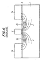
- Fig. 6 is a schematic cross sectional view illustrating a known Mach-Zehnder type optical intensity modulator comprising an X-cut LN substrate 1. Also in this known optical modulator, the electric field F is spread due to the fact that the ground electrodes 5a and 5b have a wider width than the hot electrode 4, and thus the interaction between the electric field F and the lightwave propagating along the optical waveguides 2a and 2b is decreased and a high driving voltage is required.
- the present invention has for its object to provide a novel and useful waveguide type optical modulator, which can solve the above mentioned problems of the known optical modulators, can have a wide modulation bandwidth, and can operate at a lower driving voltage.
- a waveguide type optical modulator comprising a substrate having a surface, the substrate being made of a material having an electrooptical effect, at least one optical waveguide formed in a region of said surface of said substrate and having a width W f , a buffer layer formed on the surface of the substrate, electrodes of travelling-wave type comprising a hot electrode and at least one ground electrode provided on said buffer layer for applying a microwave signal, said hot and ground electrodes being extended in parallel with said optical waveguide to modulate a lightwave being propagated along said optical waveguide, wherein said hot electrode has a width W e and an electric field adjusting planar film is provided between the buffer layer and the hot electrode, said electric field adjusting region having a width h not smaller than the width W e of the hot electrode, characterised in that the electric field adjusting planar film has a uniform width and extends along the hot electrode, and in that the width W e of the hot electrode is smaller than the width W f of said optical waveguide.
- said electric field adjusting planar film is formed above said optical waveguide and has the width h substantially equal to the width W f of the optical: waveguide.
- said electric field adjusting planar film is formed to have a non-uniform distribution of conductivity viewed in a direction of the width thereof.
- a central portion of the electric field adjusting planar film has a higher conductivity and a peripheral portion of the electric field adjusting planar film has a lower conductivity.
- a central portion of the electric field adjusting region has a lower conductivity and a peripheral portion of the electric field adjusting planar film has a higher conductivity.
- the electric field adjusting planar film may be made of a metal selected from the group consisting of Ti, Cr, Ni, Cu, Au and alloys thereof.
- said electric field adjusting planar film may be made of a semiconductive material selected from the group consisting of Ga, In, As, Al, B, Ge, Si, Sn, Sb and compounds thereof.
- a material, a thickness d and a width h of said electric field adjusting planar film are determined such that a characteristic impedance Z of said electrodes of traveling-wave type and an effective refractive index for the microwave signal are not substantially affected by the electric field adjusting region, and the interaction between the distribution of the electric field generated by the microwave signal applied to the hot electrode and the distribution of the intensity of the lightwave propagating along the optical waveguide is enhanced.
- said electric field adjusting planar film has a thickness d from 150 ⁇ to 1 ⁇ m and the width h from 2 ⁇ m to a smaller value than a sum of the width W e of the hot electrode and twice of the spacing S between the hot electrode and the ground electrode (W e + 2S).
- a waveguide type optical modulator comprising a substrate having a surface, the substrate being made of a material having an electrooptical effect, at least one optical waveguide formed in a surface region of said substrate, a buffer layer formed on the surface of the substrate, electrodes of travelling-wave type comprising a hot electrode and at least one ground electrode provided on said buffer layer for applying a microwave, said hot and ground electrodes being extended in parallel with said optical waveguide to modulate a lightwave being propagated along said optical waveguide, wherein a ground side electric field adjusting main film and a ground side electric field adjusting sub-film are provided side by side between the ground electrode and the buffer layer, characterised in that said ground side electric field adjusting main film projects towards the hot electrode from between said buffer layer and said ground electrode.
- said ground side electric field adjusting main film is made of metal, semiconductor or a combination thereof
- said ground side electric field adjusting sub-film is made of metal, semiconductor, dielectric material or a combination thereof.
- said ground side electric field adjusting sub-film is made of a dielectric material having such a dielectric constant that the interaction between the electric field and the lightwave propagating along the optical waveguide is enhanced.
- said ground side electric field adjusting main film is formed by an electrically conductive material layer, and said ground side electric field adjusting sub-region is formed by an air gap.
- the ground side electric field adjusting main film and sub-film are made of a metal selected from the group consisting of Ti, Cr, Ni, Cu, Au and alloys thereof.
- said ground side electric field adjusting main film and sub-film are made of a semiconductive material selected from the group consisting of Ga, In, As, Al, B, Ge, Si, Sn, Sb and compounds thereof.
- a material, a thickness and a width of said ground side electric field adjusting main film and sub-film are determined such that a characteristic impedance Z of said electrodes of traveling-wave type and an effective refractive index for the microwave are not substantially affected by the ground side electric field adjusting films, and an interaction between the distribution of the electric field generated by the microwave applied to the hot electrode and the distribution of the intensity of the lightwave propagating along the optical waveguide is enhanced.
- the substrate is preferably made of lithium niobate and said optical waveguide is formed by effecting a thermal diffusion of titanium into the substrate surface.
- Fig. 7 is a schematic cross sectional view showing a first embodiment of the optical modulator according to the first aspect of the invention.
- the optical modulator is formed as the Mach-Zehnder type optical intensity modulator comprising two optical waveguides and traveling-wave type electrodes.
- the optical modulator comprises a substrate 11 formed by a Z-cut lithium niobate plate having an electrooptical effect.
- optical waveguides 12a and 12b In a surface region of the substrate 11 there are formed optical waveguides 12a and 12b. These optical waveguides 12a and 12b are formed by depositing a titanium film having a thickness of 800 ⁇ and then effecting a thermal diffusion at 1000°C for ten hours.
- This buffer layer 13 is formed by a SiO 2 having a thickness of 1.0 ⁇ m and is formed by a sputtering process.
- the optical modulator comprises an electric field adjusting planar film 14 provided on the buffer layer 13.
- the electric field adjusting planar film 14 is formed by applying a photo-resist by a spin coat process, providing a mask having an opening corresponding to the electric field adjusting planar film to be formed, exposing the photo-resist through the mask and developing the photo-resist to remove an exposed portion thereof, depositing Ti by a thickness d of 500 ⁇ , and by removing the photo-resist. In this manner, the electric field adjusting planar film 14 can be formed by a lift-off method.
- the electric field adjusting planar film 14 is made of Ti, but according to the invention, the electric field adjusting planar film may be made of other material than Ti. That is to say, according to the invention, the electric field adjusting planar film 14 is made of a material selected from the group consisting of Ti, Cr, Ni, Cu and Au or alloys thereof.
- the electric field adjusting planar film 14 is formed to have a width h which is substantially equal to a width of lightwave propagating along the optical waveguide 12a.
- the electric field adjusting planar film 14 is made of Ti having a higher conductivity, and thus a width h of the region 14 is set to about 10 ⁇ m.
- the electric field adjusting region 14 may be made of a semiconductive material having a lower conductivity than metal.
- the electric field adjusting planar film 14 is made of Si, the region is preferably formed to have a thickness d of 1000 ⁇ and a width h of 20-30 ⁇ m.
- the electric field adjusting planar film 14 When the electric field adjusting planar film 14 is made of a semiconductive material, thickness d and width h of the region may be varied over a wide range, because the conductivity of the semiconductive material may be adjusted widely by selecting impurity concentration, composition and manufacturing method. However, in such a case, it is necessary to use a much more precise manufacturing machine as well as a much more strict management in manufacture.
- the semiconductive material for the electric field adjusting planar film 14 may be selected from the group consisting of Ga, In, As, Al, B, Ce, Si, Sn and Sb and compounds thereof.
- the optical modulator further comprises a hot electrode 15 and two ground electrodes 16a and 16b.
- the hot electrode 15 is provided above the first optical waveguide 12a, one of the ground electrodes 16a is provided above the second optical waveguide 12b and the other ground electrode 16b is arranged such that the ground electrodes are symmetrical with respect to the hot electrode 15.
- the hot electrode 15 and ground electrodes 16a, 16b are formed by the electroplating method using the photo-resist. That is to say, after forming the electric field adjusting planar film 14, a photo-resist is applied on the surface, portions of the applied photo-resist corresponding to the electrodes 15, 16a and 16b are selectively removed, an electrode material such as Au is deposited by an electroplating to have a thickness t of 10 ⁇ m, and finally the photo-resist is removed.
- the hot electrode 15 is formed to have a width W e such that an effective refractive index n m for the microwave signal is substantially identical to an effective refractive index no for the lightwave.
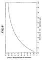
- the width W e of the hot electrode 15 is set to 5 ⁇ m which is smaller than a width W f of the optical waveguide 12a. Then, the effective refractive index for the microwave becomes about 2.2 as can be seen from a graph shown in Fig. 8.
- a horizontal axis denotes the width W e of the hot electrode 15 and a vertical axis represents the effective refractive index for the microwave.
- the effective refractive index n m for the microwave becomes about 2.5-2.6 which is larger than the effective refractive index 2.2 for the lightwave.
- the width W e of the hot electrode 15 is set to 5 ⁇ m, and thus the effective refractive index for the microwave signal is about 2.2 which is substantially equal to that for the lightwave propagating along the optical waveguides 12a and 12b. In this case, it is no more necessary to make the thickness t of the hot electrode 15 larger than an electrode spacing S.
- the velocity matching is attained between the microwave signal and the lightwave, and thus has a very wide modulation bandwidth.
- the driving voltage of the modulator becomes higher because of narrowly formed hot electrode as shown in Fig. 9.
- a horizontal axis represents the width W e of the hot electrode 15 and a vertical axis denotes a product of the half-wave voltage V ⁇ and a length L of the hot electrode.
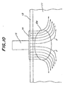
- the present embodiment has a configuration that the electric field adjusting planar film 14 is made of a suitable material having a suitable thickness d and width h such that the characteristic impedance Z of the electrodes and effective refractive index n m for the microwave signal are not affected by the electric field adjusting region 14, and at the same time, the distribution of the electric field F generated by the microwave signal applied to the hot electrode 15 and the distribution in intensity of the lightwave propagating along the optical waveguides 12a and 12b are matched with each other as illustrated in Fig. 10, and therefore a very strong interaction can be attained between the microwave electric field and the lightwave. Therefore, the driving voltage can be lowered even though the hot electrode of the modulator is formed narrowly. According to the invention, an effective width W e of the hot electrode 15 is increased by the electric field adjusting planar film 14, and thus the driving voltage can be decreased.
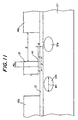
- Fig. 11 is a cross sectional view showing a second embodiment of the optical modulator according to the first aspect of the invention.
- the optical modulator of the present embodiment is also formed as the Mach-Zehnder type.
- use is made of an X-cut LN substrate 21 instead of the Z-cut LN substrate 11 used in the first embodiment.
- the maximum electro-optical constant r 33 appears horizontally, i.e. in parallel with the surface of the substrate. Therefore, the first and second optical waveguides 12a and 12b are arranged between the hot electrode 15 and the first and second ground electrodes 16a and 16b, respectively such that the electric field is horizontally applied to the lightwave propagating along the optical waveguides.
- the optical modulator of the present embodiment can be manufactured substantially in the same manner as that of the previous embodiment.
- the electric field adjusting planar film 14 is formed to have a larger width h than that of the previous embodiment. That is to say, when the electric field adjusting planar film 14 is made of NiCr, the region has a width h of 15 ⁇ m and a thickness d of 500 ⁇ .
- the electric field adjusting planar film 14 is made of a semiconductive material such as Si, it is preferable to set the thickness d and the width h of the region 14 to 1000 ⁇ and 30-40 ⁇ m, respectively. In any case, the width W e of the hot electrode 15 is set to 5 ⁇ m which is smaller than the width W f of the optical waveguides 12a and 12b.
- a thickness d of the electric field adjusting planar film 14 is preferably set to a value within a range from 150 ⁇ to 1 ⁇ m, and a width h of the electric field adjusting planar film 14 is preferably set to a value within a range from 2 ⁇ m to a value smaller than twice the sum of the electrode spacing S and the width W e of the hot electrode 15.
- Fig. 12 is a cross sectional view showing a third embodiment of the optical modulator according to the first aspect of the invention.
- the optical modulator of the present embodiment is of the Mach-Zehnder type and the Z-cut LN plate is used as a substrate 11 like as the first embodiment, and therefore, first and second optical waveguides 12a and 12b are formed under hot electrode 15 and first ground electrode 16a, respectively.
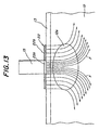
- an electric field adjusting planar film 22 provided between the buffer layer 13 and the hot electrode 15 is formed to have a non-uniform distribution in conductivity viewed in a direction parallel with the surface of the substrate 11.
- the electric field adjusting planar film 22 is consisting of a central portion 22a and a peripheral portion 22b, said central portion 22a being made of a material having a higher conductivity than a material of which the peripheral portion 22b is made. That is to say, the central portion 22a of the electric field adjusting planar film 22 is made of NiCr and the peripheral portion 22b is made of Ti, NiCr having a higher conductivity than Ti.
- the density of the electric field F generated in the vicinity of the hot electrode becomes higher at the central area and becomes lower at the peripheral area.
- the intensity distribution of lightwave propagating along the optical waveguide has the Gaussian profile in which the intensity of lightwave is weakened from the center of the intensity distribution towards the periphery as shown in Fig. 4. Therefore, the electric field can be much more effectively interacted with the lightwave propagating along the optical waveguide 12a, and thus the driving voltage can be further decreased.
- the electric field adjusting planar film 22 having the central portion 22a and peripheral portion 22b made of different materials may be manufactured in the following manner. After forming the buffer layer 13 on the substrate 11, a first photo-resist pattern having an opening at position corresponding to the central portion 22a is formed, and a NiCr film having a thickness of 1000 ⁇ is deposited by a vacuum evaporation. Then, the first photo-resist pattern is removed to form the central portion 22a having a width of 5 ⁇ m. Next, a second photo-resist pattern having an opening at a position corresponding to the peripheral portion 22b is formed and a Ti film having a thickness of 1000 ⁇ is deposited by sputtering.
- the second photo-resist pattern is removed to form the peripheral portion 22b having a width of 10 ⁇ m.
- the central portion 22a and peripheral portion 22b of the electric field adjusting planar film 22 can be easily and precisely formed by the lift-off method.
- a third photo-resist pattern having openings at positions corresponding to the hot electrode 15 and ground electrodes 16a, 16b is formed, and an Au film having a thickness of 10 ⁇ m is deposited by an electroplating.
- the third photo-resist pattern is removed to form the hot electrode 15 and ground electrodes 16a, 16b.
- the hot electrode 15 has a width W e of 5 ⁇ m smaller than a width W f of the optical waveguide 12a.
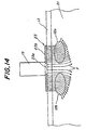
- Fig. 14 is a fourth embodiment of the optical modulator according to the first aspect of the invention.
- a substrate 21 is formed by an X-cut LN plate and thus first and second optical waveguides 12a and 12b are formed at off-set positions with respect to the hot electrode 15 like as the second embodiment illustrated in Fig. 11.
- an electric field adjusting planar film 23 is consisting of a central portion 23a made of Si and a peripheral portion 23b made of NiCr. That is to say, in the present embodiment, the central portion 23a has a lower conductivity than the peripheral portion 23b. Furthermore, the width of the central portion 23a is set to 4 ⁇ m which is smaller than the width of the hot electrode 15 of 5 ⁇ m.
- the peripheral portion 23b has a width of 10 ⁇ m and is formed to extend partially underneath the hot electrode 15. Then, the peripheral portion 23b of the electric field adjusting planar region 23 is brought in to direct contact with the hot electrode 15. Therefore, the electric field F generated in the vicinity of the hot electrode is effectively interacted with the lightwave propagating along the optical waveguides 12a and 12b as depicted in Fig. 14, and thus the driving voltage can be reduced.
- Fig. 15 is a cross sectional view showing a main portion of a fifth embodiment of the optical modulator according to the first aspect of the invention.
- a Z-cut LN substrate 11 use is made of a Z-cut LN substrate 11 and an electric field adjusting planar region 22 is formed by a central portion 22a having a width larger than that of the hot electrode 15 and a peripheral portion 22b made of a material having a lower conductivity than that of the material of the central portion 22a.
- the electric field can be effectively interacted with the lightwave propagating along the optical waveguide 12a, and thus the driving voltage can be decreased.
- Fig. 16 is a cross sectional view showing a sixth embodiment of the optical modulator according to the first aspect of the invention.
- the electric field adjusting planar film is formed such that the conductivity is changed in a stepwise manner viewed in the direction of the width thereof.
- an electric field adjusting planar film 24 is formed to have a distribution in conductivity which is gradually changed in the direction of the width thereof.
- a Si film 25 having a thickness of 1000 ⁇ and a width of 10 ⁇ m is formed on both sides of a hot electrode 15 made of Au. Then, an assembly is heated at about 350°C for three hours to form an alloy of Si and Au. In this manner, the electric field adjusting planar film 24 having the continuously changing conductivity can be obtained. In this case, a central portion of the planar film 24 has a higher conductivity than a peripheral portion.
- the electric field adjusting planar film 24 having the continuously varying distribution in conductivity is formed by the alloy of the metal and semiconductor, but according to the invention such a region may be formed by an alloy of different kinds of metals.
- Fig. 18 is a schematic cross sectional view illustrating a seventh embodiment of the optical modulator according to the second aspect of the invention.
- the optical modulator of the present embodiment is formed as a Mach-Zehnder type optical intensity modulator comprising a Z-cut LN substrate 11 having formed therein first and second optical waveguides 12a and 12b, a buffer layer 13, a hot electrode 15 and a ground electrode 31.
- a ground side electric field adjusting main films and sub-films 32 and 33 are formed between the buffer layer and the ground electrode 31, which are formed ground side electric field adjusting main films and sub-films 32 and 33, which are aligned in the direction of width of the electrode.
- the ground side electric field adjusting main film 32 is formed by a NiCr film having a thickness of 500 ⁇ .
- the ground side electric field adjusting sub-film 33 is formed by an air gap. A sufficient function may be attained by the very thin air gap 33, but in view of manufacturing, it is preferable to set a thickness of the air gap not smaller than 0.1 ⁇ m. Since the air gap 33 has a lower dielectric constant than the buffer layer 13, the effective refractive index for the microwave can be advantageously influenced by the air gap.
- the width and position of the NiCr film 32 serving as the ground side electric field adjusting main film and the width of the air gap 33 serving as the ground side electric field adjusting sub-film are determined such that the electric field F can be interacted with the lightwave propagating along the optical waveguide 12b in the most effective manner.
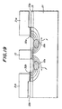
- Fig. 19 is a schematic cross sectional view showing an eighth embodiment of the optical modulator according to the second aspect of the invention.
- a substrate 21 is formed by an X-cut LN plate, and thus first and second optical waveguides 12a and 12b are formed between a hot electrode 15 and first and second ground electrodes 31a and 31b, respectively.
- first and second NiCr films 32a and 32b serving as the ground side electric field adjusting main film
- first and second air gaps 33a and 33b serving as the ground side electric field adjusting sub-films.
- the interaction between the electric field F and the lightwave propagating along the optical waveguides 12a and 12b can be enhanced, so that the driving voltage can be reduced.
- Fig. 20 is a cross sectional view depicting a ninth embodiment of the optical modulator according to the second aspect of the invention.
- a Z-cut LN substrate 11 is used, and thus first and second optical waveguides 12a and 12b are formed under hot electrode 15 and first ground electrode 34a, respectively.
- a second ground electrode 34b is formed at the opposite side to the first ground electrode 34a with respect to the hot electrode 15.
- first and second ground side electric field adjusting main films 35a and 35b as well as first and second ground side electric field adjusting sub-regions 36a and 36b.
- Each of the first and second ground side electric field adjusting main films regions 35a and 35b are consisting of a NiCr film having a thickness of 500 ⁇ and a width of 10 ⁇ m which is substantially equal to a width of the optical waveguide 12b.
- Each of the first and second ground side electric field adjusting sub-films 36a and 36b are consisting of a Ti film having a thickness of 500 ⁇ and a width of 300 ⁇ m.
- These regions 35a, 35b, 36a and 36b may be manufactured by the lift-off method using photo-resist patterns.
- the hot electrode 15 and ground electrodes 34a and 34b are formed by an Au film having a thickness of 10 ⁇ m. These electrodes may be formed by using the electroplating process. It should be noted that the hot electrode 15 has a width of 5 ⁇ m which is smaller than the width of the optical waveguide 12a such that desired velocity matching between the microwave signal and the lightwave can be attained.
- the improvement of the interaction between the microwave electric field and the lightwave propagating along the optical waveguide 12b can be attained by providing only the ground side electric field adjusting main-films and sub-films 35a and 36a underneath the first ground electrode 34a.
- a cross section of the optical modulator preferably has a symmetrical construction, and therefore it is preferable to provide the second ground side electric field adjusting main films and sub-films 35b and 36b underneath the second ground electrode 34b as shown in Fig. 20.
- NiCr of the ground side electric field adjusting main film 35a has a higher conductivity than Ti of the ground side electric field adjusting sub-film 36a, and thus the electric field intensity becomes higher at the ground side electric field adjusting main-region film 35a. Therefore, the interaction between the electric field and the lightwave propagating along the optical waveguide 12b is enhanced.
- Fig. 21 is a cross sectional view showing a tenth embodiment of the optical modulator according to the second aspect of the invention.
- each of first and second ground side electric field adjusting main-films are consisting of a central portion 37a, 37b made of NiCr and a peripheral portion 38a, 38b made of Ti, and each of first and second ground side electric field adjusting sub-films 39a, 39b are made of Si. Then, the electric field intensity is increased at a center of the optical waveguide 12b, and thus the function of the electric field is further enhanced.
- the ground side electric field adjusting main-films and sub-films may have various constructions.
- these regions may be consisting of more than three different kinds of materials or may be constructed as a film having a continuously changing conductivity like as the electric field adjusting region formed between the buffer layer and the hot electrode.
- Such a region may be formed by an alloy of metals or an alloy of metal and semiconductor.
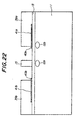
- Fig. 22 is a cross sectional view illustrating an eleventh embodiment of the optical modulator according to the second aspect of the invention.
- ground side electric field adjusting main films and sub-film 40a, 41a; 40b, 41b are formed between the buffer layer 13 and a part of ground electrodes 39a, 39b. That is to say, the ground electrodes 39a and 39b are partially brought into direct contact with the buffer layer 13.
- Fig. 23 is a cross sectional view depicting a twelfth embodiment of the optical modulator according to the second aspect of the invention.
- ground side electric field adjusting main films 42a and 42b are provided between the buffer layer 13 and the ground electrodes 34a and 34b, respectively. These regions 42a and 42b are formed by a NiCr film having a thickness of 0.1 ⁇ m.
- Ground side electric field adjusting sub-film 43a and 43b are formed by air gaps having a thickness of 0.1 ⁇ m.
- Fig. 24 is a cross sectional view showing a thirteenth embodiment of the optical modulator according to the second aspect of the invention.
- ground side electric field adjusting sub-film 43a and 43b are formed by air gaps having a thickness equal to that of the metal film constituting ground side electric field adjusting main films 42a and 42b, but ground electrodes 44a and 44b have projections formed in rear surfaces thereof, said projections having a height equal to the thickness of air gaps. Then, the ground electrodes 44a and 44b are supported on the buffer layer 13 by means of the ground side electric field adjusting films 42a, 42b and the projections.
- Fig. 25 is a cross sectional view illustrating a fourteenth embodiment of the optical modulator according to the second aspect of the invention.
- projections 45a and 45b which serve as the ground side electric field adjusting sub-films.
- Ground side electric field adjusting films 46a and 46b are formed by a metal film having a thickness which is smaller than the height of the projections 45a and 45b. Therefore, ground electrodes 47a and 47b have complemental projections formed in lower surfaces thereof corresponding inversely to the projections of the buffer layer 45a and 45b.
- Fig. 26 is a schematic cross sectional view depicting a fifteenth embodiment of the optical modulator according to a combination of the above mentioned first and second aspects of the invention.
- an electric field adjusting film 14 made of Ti like as in the first embodiment shown in Fig. 7, and at the same time, between the buffer layer 13 and the ground electrode 31 are provided the ground side electric field adjusting main films and sub-films 32 and 33.
- the ground side electric field adjusting main-film 32 is made of NiCr and the sub-region 33 is formed by the air gap just like as the eight embodiment depicted in Fig. 19.
- Fig. 27 is a cross sectional view showing a sixteenth embodiment of the optical modulator according to a combination of the first and second aspects.
- the electric field adjusting film 22 provided between the buffer layer 13 and the hot electrode 15 is consisting of a central portion 22a made of NiCr and a peripheral portion 22b made of Ti like as the third embodiment shown in Fig. 12.
- the ground electrodes 34a, 34b and the buffer layer 13 there are provided ground side electric field adjusting main-films 35a, 35b made of NiCr and ground side electric field adjusting sub-films 36a, 36b made of Ti like as the ninth embodiment depicted in Fig. 20.
- the electric field is concentrated in the vicinity of both the first and second optical waveguides 12a and 12b, and therefore the interaction between the electric field and the lightwave propagating along these waveguides is enhanced very much and the driving voltage can be decreased very much.
- the effective refractive index for the microwave becomes substantially identical to that for the lightwave without affecting the characteristic impedance Z and frequency characteristic of the optical modulator.
- the optical modulator is constructed as the Mach-Zehnder type having the first and second optical waveguides.
- it is also possible to construct the optical modulator in any other type than the Mach-Zehnder type.
- Fig. 28 is a cross sectional view showing a seventeenth embodiment of the optical modulator according to the invention.
- a surface region of a Z-cut LN substrate 11 is formed only a single optical waveguide 12 by effecting a thermal diffusion of Ti.
- a buffer layer 13 On the surface of the substrate 11, there is formed a buffer layer 13.
- An electric field adjusting film 14 made of NiCr is deposited on the buffer layer 13 at position immediately above the optical waveguide 12. Further, on the electric field adjusting film 14 is formed a hot electrode 15.
- the electric field adjusting film 14 is formed to have a width h which is substantially equal to the width W f of the optical waveguide 12 and the hot electrode 15 is formed to have a width W e which is smaller than the width W f of the optical waveguide 12. Further, it is no more necessary to make the thickness t of the hot electrode 15 and ground electrodes 16a and 16b larger than the electrode spacing S. Moreover, the thickness d of the electric field adjusting film 14 is set to a value within a range from 150 ⁇ to 1000 ⁇ , which is sufficiently smaller than the thickness t of the hot electrode 15.
- the optical modulator shown in Fig. 28 may be used as an optical phase modulator or a polarization scrambler.
- the substrate is formed by the Z-cut or X-cut LN plate, but according to the invention, it is also possible to use a Y-cut LN plate.
- the substrate may be made of a dielectric or semiconductive material having the electrooptical effect other than lithium niobate.
- the optical modulator with optical waveguide which can solve the above mentioned problems of the known optical modulators such as the problem of peeling off of the thick hot electrode, the problem of varying the characteristic impedance, frequency characteristic and effective refractive index for the microwave signal. Further, the optical modulator according to the invention has a wide modulation bandwidth and an excellent impedance matching.
- the electric field generated by applied microwave can be concentrated to the vicinity of the optical waveguide and, therefore, the interaction between the electric field and the lightwave propagating along the optical waveguide can be enhanced. Therefore, the driving voltage can be decreased.
Landscapes
- Physics & Mathematics (AREA)
- Nonlinear Science (AREA)
- Electromagnetism (AREA)
- Chemical & Material Sciences (AREA)
- Engineering & Computer Science (AREA)
- Ceramic Engineering (AREA)
- Crystallography & Structural Chemistry (AREA)
- General Physics & Mathematics (AREA)
- Optics & Photonics (AREA)
- Optical Modulation, Optical Deflection, Nonlinear Optics, Optical Demodulation, Optical Logic Elements (AREA)
- Optical Integrated Circuits (AREA)
Description
- The present invention relates to a waveguide type optical modulator for use in an optical fiber communication system of high capacity and high speed, and more particularly relates to a waveguide-type optical modulator which has desired characteristic impedance and effective refractive index for a microwave signal and can operate at a high speed with a low driving voltage.
- In a recent high capacity and high speed optical fiber communication system, an external modulator has been utilized instead of a direct modulator in which a laser diode is directly modulated. In the external modulator, there has been proposed a waveguide-type optical modulator, in which a waveguide is formed in a substrate made of a material having an electrooptical effect such as lithium niobate LiNbO3, hereinbelow called LN for the sake of simplicity. In one of known waveguide type external optical modulators, traveling-wave type electrodes are provided on a surface of the substrate along the optical waveguide.
- In the waveguide type optical modulator having the traveling-wave type electrode, it is necessary to suppress undesired reflection of an electric signal as much as possible. To this end, the characteristic impedance of the optical modulator should be matched to that of a driver for operating the modulator. Usually, the characteristic impedance of the driver is 50 Ω, and thus the characteristic impedance of the optical modulator has to be set to 50 Ω. Moreover, in order to broaden the modulation bandwidth, the traveling velocity of a microwave signal across the hot electrode should be made identical with the velocity of lightwave propagating along the optical waveguide as much as possible. That is to say, velocity matching is important. However, since LN has a very large dielectric constant, a velocity of the microwave signal traveling across the hot electrode is lower than that of the lightwave, and thus the velocity matching could be hardly attained.
- There have been proposed prior art techniques for solving the above mentioned problems. For instance, Japanese Patent Publication No. 7-13711, Japanese Patent Application Laid-open Publication No. 2-51123 and Japanese Patent Application Laid-open Publication No. 2-93423 have taught several solutions. In these prior art publications, in order to satisfy the velocity matching by decreasing an effective refractive index for the microwave signal, the thickness of the hot electrode is increased, the thickness of a buffer layer is increased, a recess is formed in the substrate surface between the electrodes, or an overhang is formed in a surface of the electrode.
- Fig. 1A is a perspective view showing a known external modulation type optical modulator and Fig. 1B is a cross sectional view cut along a line A-A in Fig. 1A. This known external type optical modulator is a Mach-Zehnder type intensity modulator having two optical waveguides. The optical modulator comprises a
substrate 1 made of a material having an electro-optical effect. In this example, thesubstrate 1 is formed by a Z-cut plate of LN. In a surface region of thesubstrate 1 there are formed twooptical waveguides optical waveguides optical waveguides optical fiber 6 is optically coupled with the input sideoptical waveguide 2c and a laminated polarizer 7 is inserted between the input sideoptical fiber 6 and the input sideoptical waveguide 2c. An output sideoptical fiber 8 is optically coupled with the output sideoptical waveguide 2d. Theoptical waveguides 2a-2d are formed by effecting a thermal diffusion of Ti into the surface of thesubstrate 1. On the surface of thesubstrate 1, abuffer layer 3 is formed, and onehot electrode 4 and twoground electrodes buffer layer 3. An input side end of thehot electrode 4 is connected to a microwave signal source 9 and an output side end of the hot electrode is connected to aterminal resistor 10 of 50 Ω. - Among the electrooptical constants of the
LN substrate 1, r33 is the largest one and therefore this is most effective when an electric field is applied in the Z direction of thesubstrate 1, i.e. a direction of the thickness. Therefore, thehot electrode 4 is provided above theoptical waveguide 2a as shown in Fig. 1B, so that the electric field is effectively applied to the optical waveguide in the Z direction. Thehot electrode 4 has a width We which is substantially equal to the width Wf of theoptical waveguide 2a for enhancing an interaction between the lightwave propagating along the optical waveguide and the electric field of the microwave. - Figs. 2 and 3 are schematic cross sectional views showing the interaction between the lightwave propagating along the
optical waveguide 2a and the electric field F. In Fig. 2, the width We of thehot electrode 4 is substantially equal to the width Wf of theoptical waveguide 2a, and in Fig. 3, the width We of thehot electrode 4 is smaller than the width Wf of theoptical waveguide 2a. In Fig. 2, the electric field F effectively traverses theoptical waveguide 2a and there is produced a strong interaction between the lightwave and the electric field F. Because the amplitude of the driving voltage of the microwave is determined by the degree of the interaction, the arrangement shown in Fig. 2 is a preferable configuration for lower driving voltage than that shown in Fig. 3. In this manner, thehot electrode 4 should have a width We substantially identical with that of theoptical waveguide 2a. - The width Wf of the
optical waveguide 2a is dependent upon process condition of the waveguide and the wavelength of the lightwave propagating along the optical waveguide and is about 10 µm for the single mode optical waveguide of Ti diffusion type having a wavelength λ=1.5 µm. - Fig. 4 is a typical profile representing an intensity distribution of lightwave propagating along the
optical waveguide 2a- In case of forming theoptical waveguide 2a by effecting a thermal diffusion of Ti into theLN substrate 1, the intensity distribution of lightwave becomes a Gaussian type. From Fig. 4, it can be derived that the whole width of the lightwave propagating along theoptical waveguide 2a is reached at about 20 µm, although the intensity of lightwave is decreased by 1/e2 at a width in 10 µm. - On the other hand, in the known optical modulator, the
hot electrode 4 has a large thickness t in order to make the velocity of the microwave signal closer to that of the lightwave. That is to say, when the hot electrode has a large thickness t, an effective refractive index for the microwave is decreased so as to attain the velocity matching. - The effective refractive index nm for the microwave is affected by the large dielectric constant of the
LN substrate 1 and becomes about 4.2 when the thickness t of the hot electrode is small. On the other hand, the effective refractive index no for the lightwave is about 2.2. By increasing the thickness t of thehot electrode 4, the effective refractive index for the microwave is decreased toward 2.2 because a thickly formed electrode having larger surface area decreases the effective dielectric constant for the microwave signal. - As explained above, in the known optical modulator, in order to reduce the effective refractive index for the microwave from 4.2 to 2.2, the thickness t of the
hot electrode 4 has to be made larger than the spacing S between thehot electrode 4 and theground electrode 5a or the width We of thehot electrode 4 has to be narrowed. - In general, the spacing S between the
hot electrode 4 having a width We of 10 µm and theground electrodes hot electrode 4 larger than the electrode spacing S, thehot electrode 4 has to be formed by depositing Au by electroplating more than 30 µm. - However, in practice, it is very difficult to form such a thick electrode larger than the electrode spacing S. Moreover, there might occur a problem of peeling off of the electrode due to an internal stress produced within the deposited Au electrode. Furthermore, it is also difficult to manufacture the hot electrode having a desired cross sectional configuration reliably, and thus the characteristic impedance of the optical modulator and effective refractive index for the microwave signal might fluctuate. Moreover, a known solution of providing the hot electrode with the overhung portion could not be easily adopted due to a limitation of the fine treating, and the above mentioned problems might also occur.
- The effective refractive index for the microwave can be reduced by increasing the thickness of the
buffer layer 3. However, this might cause another problem namely, that a higher driving voltage is required. Moreover, if the effective refractive index for the microwave is decreased by reducing the width We of thehot electrode 4, the driving voltage might be increased. - In the known solution in which the recesses are formed in the substrate between the hot electrode and the ground electrodes for decreasing the effective refractive index for the microwave signal, a manufacturing process becomes very complicated and requires a large machine. Moreover, the formation of recesses might damage the substrate and buffer layer.
- In the known optical modulator, the
ground electrode 5a has a width sufficiently larger than that of thehot electrode 4, and thus lines of electric force are spread under theground electrode 5a and the electric field density is lower than that under thehot electrode 4 as illustrated in Fig. 5. Therefore, the interaction between the electric field F and the lightwave propagating along theoptical waveguides optical waveguides optical waveguides ground electrode 5a may be decreased or the spacing between thehot electrode 4 and theground electrode 5a may be reduced. However, then another problem might occur, namely that a frequency characteristic might be deteriorated particularly at a high frequency and a deviation of the characteristic impedance might occur so that undesired reflections increase. - Japanese publication number JP-A-4268531 discloses a known optical waveguide device with the features forming the preamble of
claim 1 and corresponding to a first aspect of the invention. In particular, JP-A-4268531 discloses a modulator wherein the hot electrode is provided with a plurality of metallic projections formed under the hot electrode. - Japanese publication number JP-06235B91 discloses a known optical waveguide device with the features forming the preamble of claim 17 and corresponding to a second aspect of the present invention. In particular, JP-06235891 discloses a modulator wherein the ground electrode has a cross-section formed by two different materials, in order to concentrate the electric field under the ground electrode.
- Fig. 6 is a schematic cross sectional view illustrating a known Mach-Zehnder type optical intensity modulator comprising an
X-cut LN substrate 1. Also in this known optical modulator, the electric field F is spread due to the fact that theground electrodes hot electrode 4, and thus the interaction between the electric field F and the lightwave propagating along theoptical waveguides - The present invention has for its object to provide a novel and useful waveguide type optical modulator, which can solve the above mentioned problems of the known optical modulators, can have a wide modulation bandwidth, and can operate at a lower driving voltage.
- It is another object of the invention to provide a novel and useful waveguide type optical modulator, in which the spread of the electric field under the ground electrode can be reduced and, thus the interaction between the electric field and the lightwave propagating along the optical waveguide under or near the ground electrode can be increased so that the driving voltage can be lowered.
- According to a first aspect of the invention, a waveguide type optical modulator comprising a substrate having a surface, the substrate being made of a material having an electrooptical effect, at least one optical waveguide formed in a region of said surface of said substrate and having a width Wf, a buffer layer formed on the surface of the substrate, electrodes of travelling-wave type comprising a hot electrode and at least one ground electrode provided on said buffer layer for applying a microwave signal, said hot and ground electrodes being extended in parallel with said optical waveguide to modulate a lightwave being propagated along said optical waveguide, wherein said hot electrode has a width We and an electric field adjusting planar film is provided between the buffer layer and the hot electrode, said electric field adjusting region having a width h not smaller than the width We of the hot electrode, characterised in that the electric field adjusting planar film has a uniform width and extends along the hot electrode, and in that the width We of the hot electrode is smaller than the width Wf of said optical waveguide.
- According to a preferable embodiment of the first aspect of the invention, said electric field adjusting planar film is formed above said optical waveguide and has the width h substantially equal to the width Wf of the optical: waveguide.
- According to another preferable embodiment of the first aspect of the invention, said electric field adjusting planar film is formed to have a non-uniform distribution of conductivity viewed in a direction of the width thereof.
- When the optical waveguide is formed below the hot electrode, a central portion of the electric field adjusting planar film has a higher conductivity and a peripheral portion of the electric field adjusting planar film has a lower conductivity. When the optical waveguide is formed between the hot electrode and the ground electrode, a central portion of the electric field adjusting region has a lower conductivity and a peripheral portion of the electric field adjusting planar film has a higher conductivity.
- According to the first aspect of the invention, the electric field adjusting planar film may be made of a metal selected from the group consisting of Ti, Cr, Ni, Cu, Au and alloys thereof.
- Furthermore, said electric field adjusting planar film may be made of a semiconductive material selected from the group consisting of Ga, In, As, Al, B, Ge, Si, Sn, Sb and compounds thereof.
- According to the first aspect of the invention, a material, a thickness d and a width h of said electric field adjusting planar film are determined such that a characteristic impedance Z of said electrodes of traveling-wave type and an effective refractive index for the microwave signal are not substantially affected by the electric field adjusting region, and the interaction between the distribution of the electric field generated by the microwave signal applied to the hot electrode and the distribution of the intensity of the lightwave propagating along the optical waveguide is enhanced.
- In a preferable embodiment of the optical modulator according to the first aspect of the invention, said electric field adjusting planar film has a thickness d from 150 Å to 1µm and the width h from 2 µm to a smaller value than a sum of the width We of the hot electrode and twice of the spacing S between the hot electrode and the ground electrode (We + 2S).
- According to a second aspect of the invention, a waveguide type optical modulator comprising a substrate having a surface, the substrate being made of a material having an electrooptical effect, at least one optical waveguide formed in a surface region of said substrate, a buffer layer formed on the surface of the substrate, electrodes of travelling-wave type comprising a hot electrode and at least one ground electrode provided on said buffer layer for applying a microwave, said hot and ground electrodes being extended in parallel with said optical waveguide to modulate a lightwave being propagated along said optical waveguide, wherein a ground side electric field adjusting main film and a ground side electric field adjusting sub-film are provided side by side between the ground electrode and the buffer layer, characterised in that said ground side electric field adjusting main film projects towards the hot electrode from between said buffer layer and said ground electrode.
- In a preferable embodiment according to the second aspect of the invention, said ground side electric field adjusting main film is made of metal, semiconductor or a combination thereof, and said ground side electric field adjusting sub-film is made of metal, semiconductor, dielectric material or a combination thereof.
- In a preferable embodiment according to the second aspect of the invention, said ground side electric field adjusting sub-film is made of a dielectric material having such a dielectric constant that the interaction between the electric field and the lightwave propagating along the optical waveguide is enhanced.
- In another preferable embodiment according to the second aspect of the invention, said ground side electric field adjusting main film is formed by an electrically conductive material layer, and said ground side electric field adjusting sub-region is formed by an air gap.
- In a preferable embodiment according to the second aspect of the invention, the ground side electric field adjusting main film and sub-film are made of a metal selected from the group consisting of Ti, Cr, Ni, Cu, Au and alloys thereof.
- In another preferable embodiment according to the second aspect of the invention, said ground side electric field adjusting main film and sub-film are made of a semiconductive material selected from the group consisting of Ga, In, As, Al, B, Ge, Si, Sn, Sb and compounds thereof.
- According to the second aspect of the invention, a material, a thickness and a width of said ground side electric field adjusting main film and sub-film are determined such that a characteristic impedance Z of said electrodes of traveling-wave type and an effective refractive index for the microwave are not substantially affected by the ground side electric field adjusting films, and an interaction between the distribution of the electric field generated by the microwave applied to the hot electrode and the distribution of the intensity of the lightwave propagating along the optical waveguide is enhanced.
- According to the invention, the substrate is preferably made of lithium niobate and said optical waveguide is formed by effecting a thermal diffusion of titanium into the substrate surface.
-
- Figs. 1A and 1B are perspective and cross sectional views, respectively showing a known optical modulator of waveguide type;
- Fig. 2 is a schematic cross sectional view illustrating the distribution of the electric field with respect to the optical waveguides in the known optical modulator shown in Fig. 1;
- Fig. 3 is a schematic cross sectional view depicting the distribution of the electric field in another known optical modulator of waveguide type;
- Fig. 4 is a typical profile illustrating an intensity distribution of the lightwave propagating along the optical waveguide in the known optical modulator;
- Fig. 5 is a schematic cross sectional view showing the distribution of the electric field in the known optical modulator;
- Fig. 6 is a schematic cross sectional view depicting the distribution of the electric field in another known optical modulator;
- Fig. 7 is a schematic cross sectional view illustrating a first embodiment of the optical modulator according to the invention;
- Fig. 8 is a graph representing a simulated relationship between a width of the hot electrode and an effective refractive index for the microwave;
- Fig. 9 is a graph expressing a simulated relationship between a width of the hot electrode and a driving voltage;
- Fig. 10 is a schematic cross sectional view representing the distribution of the electric field in the optical modulator shown in Fig. 7;
- Fig. 11 is a cross sectional view illustrating a second embodiment of the optical modulator according to the invention;
- Fig. 12 is a cross sectional view showing a third embodiment of the optical modulator according to the invention;
- Fig. 13 is an enlarged cross sectional view of a hot electrode portion of Fig. 12;
- Fig. 14 is a cross sectional view depicting a fourth embodiment of the optical modulator according to the invention;
- Fig. 15 is a cross sectional view illustrating a main portion of a fifth embodiment of the optical modulator according to the invention;
- Fig. 16 is a cross sectional view showing a main portion of a sixth embodiment of the optical modulator according to the invention;
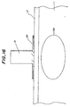
- Fig. 17 is a cross sectional view for explaining a method of manufacturing the optical modulator shown in Fig. 16:
- Fig. 18 is a schematic cross sectional view depicting a seventh embodiment of the optical modulator according to the invention;
- Fig. 19 is a schematic cross sectional view illustrating an eighth embodiment of the optical modulator according to the invention;
- Fig. 20 is a cross sectional view showing a ninth embodiment of the optical modulator according to the invention
- Fig. 21 is a cross sectional view illustrating a tenth embodiment of the optical modulator according to the invention
- Fig. 22 is a cross sectional view depicting an eleventh embodiment of the optical modulator according to the invention;
- Fig. 23 is a cross sectional view showing a twelfth embodiment of the optical modulator according to the invention;
- Fig. 24 is a cross sectional view representing a thirteenth embodiment of the optical modulator according to the invention;
- Fig. 25 is a cross sectional view depicting a fourteenth embodiment of the optical modulator according to the invention;
- Fig. 26 is a schematic cross sectional view illustrating a fifteenth embodiment of the optical modulator according to the invention;
- Fig. 27 is a cross sectional view showing a sixteenth embodiment of the optical modulator according to the invention; and
- Fig. 28 is a cross sectional view expressing a seventeenth embodiment of the optical modulator according to the invention.
- Fig. 7 is a schematic cross sectional view showing a first embodiment of the optical modulator according to the first aspect of the invention. In the present embodiment, the optical modulator is formed as the Mach-Zehnder type optical intensity modulator comprising two optical waveguides and traveling-wave type electrodes. The optical modulator comprises a substrate 11 formed by a Z-cut lithium niobate plate having an electrooptical effect. In a surface region of the substrate 11 there are formed
optical waveguides optical waveguides buffer layer 13 for suppressing lightwave absorption by metal electrodes. Thisbuffer layer 13 is formed by a SiO2 having a thickness of 1.0 µm and is formed by a sputtering process. - The optical modulator comprises an electric field adjusting
planar film 14 provided on thebuffer layer 13. The electric field adjustingplanar film 14 is formed by applying a photo-resist by a spin coat process, providing a mask having an opening corresponding to the electric field adjusting planar film to be formed, exposing the photo-resist through the mask and developing the photo-resist to remove an exposed portion thereof, depositing Ti by a thickness d of 500 Å, and by removing the photo-resist. In this manner, the electric field adjustingplanar film 14 can be formed by a lift-off method. - In the present embodiment, the electric field adjusting
planar film 14 is made of Ti, but according to the invention, the electric field adjusting planar film may be made of other material than Ti. That is to say, according to the invention, the electric field adjustingplanar film 14 is made of a material selected from the group consisting of Ti, Cr, Ni, Cu and Au or alloys thereof. - The electric field adjusting
planar film 14 is formed to have a width h which is substantially equal to a width of lightwave propagating along theoptical waveguide 12a. In the present embodiment, the electric field adjustingplanar film 14 is made of Ti having a higher conductivity, and thus a width h of theregion 14 is set to about 10 µm. The electricfield adjusting region 14 may be made of a semiconductive material having a lower conductivity than metal. When the electric field adjustingplanar film 14 is made of Si, the region is preferably formed to have a thickness d of 1000 Å and a width h of 20-30 µm. - When the electric field adjusting
planar film 14 is made of a semiconductive material, thickness d and width h of the region may be varied over a wide range, because the conductivity of the semiconductive material may be adjusted widely by selecting impurity concentration, composition and manufacturing method. However, in such a case, it is necessary to use a much more precise manufacturing machine as well as a much more strict management in manufacture. The semiconductive material for the electric field adjustingplanar film 14 may be selected from the group consisting of Ga, In, As, Al, B, Ce, Si, Sn and Sb and compounds thereof. - The optical modulator further comprises a
hot electrode 15 and twoground electrodes hot electrode 15 is provided above the firstoptical waveguide 12a, one of theground electrodes 16a is provided above the secondoptical waveguide 12b and theother ground electrode 16b is arranged such that the ground electrodes are symmetrical with respect to thehot electrode 15. - The
hot electrode 15 andground electrodes planar film 14, a photo-resist is applied on the surface, portions of the applied photo-resist corresponding to theelectrodes - The
hot electrode 15 is formed to have a width We such that an effective refractive index nm for the microwave signal is substantially identical to an effective refractive index no for the lightwave. In the present embodiment, the width We of thehot electrode 15 is set to 5 µm which is smaller than a width Wf of theoptical waveguide 12a. Then, the effective refractive index for the microwave becomes about 2.2 as can be seen from a graph shown in Fig. 8. In Fig. 8, a horizontal axis denotes the width We of thehot electrode 15 and a vertical axis represents the effective refractive index for the microwave. When the hot electrode has a width We of 10-20 µm as the known optical modulator, the effective refractive index nm for the microwave becomes about 2.5-2.6 which is larger than the effective refractive index 2.2 for the lightwave. In the present embodiment, the width We of thehot electrode 15 is set to 5 µm, and thus the effective refractive index for the microwave signal is about 2.2 which is substantially equal to that for the lightwave propagating along theoptical waveguides hot electrode 15 larger than an electrode spacing S. Therefore, it is possible to overcome the problems of the known optical modulator such as the peeling off of the hot electrode due to an internal stress of the thick metal deposition and the variation in the impedance of the optical modulator and in the effective refractive index for the microwave due to a poor reproducibility of the thick hot electrode. - In the Mach-Zehnder type optical intensity modulator having the very narrow hot electrode of the present embodiment, the velocity matching is attained between the microwave signal and the lightwave, and thus has a very wide modulation bandwidth. However, there occurs a problem that the driving voltage of the modulator becomes higher because of narrowly formed hot electrode as shown in Fig. 9. In Fig. 9, a horizontal axis represents the width We of the
hot electrode 15 and a vertical axis denotes a product of the half-wave voltage Vπ and a length L of the hot electrode. To overcome this problem, the present embodiment has a configuration that the electric field adjustingplanar film 14 is made of a suitable material having a suitable thickness d and width h such that the characteristic impedance Z of the electrodes and effective refractive index nm for the microwave signal are not affected by the electricfield adjusting region 14, and at the same time, the distribution of the electric field F generated by the microwave signal applied to thehot electrode 15 and the distribution in intensity of the lightwave propagating along theoptical waveguides hot electrode 15 is increased by the electric field adjustingplanar film 14, and thus the driving voltage can be decreased. - Fig. 11 is a cross sectional view showing a second embodiment of the optical modulator according to the first aspect of the invention. The optical modulator of the present embodiment is also formed as the Mach-Zehnder type. In the present embodiment, use is made of an
X-cut LN substrate 21 instead of the Z-cut LN substrate 11 used in the first embodiment. In theX-cut LN substrate 21, the maximum electro-optical constant r33 appears horizontally, i.e. in parallel with the surface of the substrate. Therefore, the first and secondoptical waveguides hot electrode 15 and the first andsecond ground electrodes X-cut LN substrate 21, the electric field adjustingplanar film 14 is formed to have a larger width h than that of the previous embodiment. That is to say, when the electric field adjustingplanar film 14 is made of NiCr, the region has a width h of 15 µm and a thickness d of 500 Å. This is due to a fact that when theoptical waveguides electrodes electrodes planar film 14, and thus the driving voltage can be lowered. - When the electric field adjusting
planar film 14 is made of a semiconductive material such as Si, it is preferable to set the thickness d and the width h of theregion 14 to 1000 Å and 30-40 µm, respectively. In any case, the width We of thehot electrode 15 is set to 5 µm which is smaller than the width Wf of theoptical waveguides - According to the invention, it has been experimentally confirmed that a thickness d of the electric field adjusting
planar film 14 is preferably set to a value within a range from 150 Å to 1 µm, and a width h of the electric field adjustingplanar film 14 is preferably set to a value within a range from 2 µm to a value smaller than twice the sum of the electrode spacing S and the width We of thehot electrode 15. - Fig. 12 is a cross sectional view showing a third embodiment of the optical modulator according to the first aspect of the invention. The optical modulator of the present embodiment is of the Mach-Zehnder type and the Z-cut LN plate is used as a substrate 11 like as the first embodiment, and therefore, first and second
optical waveguides hot electrode 15 andfirst ground electrode 16a, respectively. According to this aspect of the invention, an electric field adjustingplanar film 22 provided between thebuffer layer 13 and thehot electrode 15 is formed to have a non-uniform distribution in conductivity viewed in a direction parallel with the surface of the substrate 11. In the present embodiment, the electric field adjustingplanar film 22 is consisting of acentral portion 22a and aperipheral portion 22b, saidcentral portion 22a being made of a material having a higher conductivity than a material of which theperipheral portion 22b is made. That is to say, thecentral portion 22a of the electric field adjustingplanar film 22 is made of NiCr and theperipheral portion 22b is made of Ti, NiCr having a higher conductivity than Ti. - Then, as illustrated in Fig. 13, the density of the electric field F generated in the vicinity of the hot electrode becomes higher at the central area and becomes lower at the peripheral area. On the other hand, the intensity distribution of lightwave propagating along the optical waveguide has the Gaussian profile in which the intensity of lightwave is weakened from the center of the intensity distribution towards the periphery as shown in Fig. 4. Therefore, the electric field can be much more effectively interacted with the lightwave propagating along the
optical waveguide 12a, and thus the driving voltage can be further decreased. - The electric field adjusting
planar film 22 having thecentral portion 22a andperipheral portion 22b made of different materials may be manufactured in the following manner. After forming thebuffer layer 13 on the substrate 11, a first photo-resist pattern having an opening at position corresponding to thecentral portion 22a is formed, and a NiCr film having a thickness of 1000 Å is deposited by a vacuum evaporation. Then, the first photo-resist pattern is removed to form thecentral portion 22a having a width of 5 µm. Next, a second photo-resist pattern having an opening at a position corresponding to theperipheral portion 22b is formed and a Ti film having a thickness of 1000 Å is deposited by sputtering. After that, the second photo-resist pattern is removed to form theperipheral portion 22b having a width of 10 µm. In this manner, thecentral portion 22a andperipheral portion 22b of the electric field adjustingplanar film 22 can be easily and precisely formed by the lift-off method. Then, a third photo-resist pattern having openings at positions corresponding to thehot electrode 15 andground electrodes hot electrode 15 andground electrodes hot electrode 15 has a width We of 5 µm smaller than a width Wf of theoptical waveguide 12a. - Fig. 14 is a fourth embodiment of the optical modulator according to the first aspect of the invention. In the present embodiment, a
substrate 21 is formed by an X-cut LN plate and thus first and secondoptical waveguides hot electrode 15 like as the second embodiment illustrated in Fig. 11. Also in the present embodiment, an electric field adjustingplanar film 23 is consisting of acentral portion 23a made of Si and a peripheral portion 23b made of NiCr. That is to say, in the present embodiment, thecentral portion 23a has a lower conductivity than the peripheral portion 23b. Furthermore, the width of thecentral portion 23a is set to 4 µm which is smaller than the width of thehot electrode 15 of 5 µm. The peripheral portion 23b has a width of 10 µm and is formed to extend partially underneath thehot electrode 15. Then, the peripheral portion 23b of the electric field adjustingplanar region 23 is brought in to direct contact with thehot electrode 15. Therefore, the electric field F generated in the vicinity of the hot electrode is effectively interacted with the lightwave propagating along theoptical waveguides - Fig. 15 is a cross sectional view showing a main portion of a fifth embodiment of the optical modulator according to the first aspect of the invention. In the present embodiment, use is made of a Z-cut LN substrate 11 and an electric field adjusting
planar region 22 is formed by acentral portion 22a having a width larger than that of thehot electrode 15 and aperipheral portion 22b made of a material having a lower conductivity than that of the material of thecentral portion 22a. Also in the present embodiment, the electric field can be effectively interacted with the lightwave propagating along theoptical waveguide 12a, and thus the driving voltage can be decreased. - Fig. 16 is a cross sectional view showing a sixth embodiment of the optical modulator according to the first aspect of the invention. In the embodiments depicted in Figs. 12-15, the electric field adjusting planar film is formed such that the conductivity is changed in a stepwise manner viewed in the direction of the width thereof. However, in the present embodiment, an electric field adjusting
planar film 24 is formed to have a distribution in conductivity which is gradually changed in the direction of the width thereof. By suitably selecting the distribution in conductivity of the electric field adjustingplanar film 24, it is possible to further enhance the interaction between the electric field and the lightwave, and therefore the driving voltage can be further decreased. - Now an example of a method of manufacturing the electric field adjusting
planar film 24 having the continuously changing distribution in conductivity will be explained. At first, as depicted in Fig. 17, aSi film 25 having a thickness of 1000 Å and a width of 10 µm is formed on both sides of ahot electrode 15 made of Au. Then, an assembly is heated at about 350°C for three hours to form an alloy of Si and Au. In this manner, the electric field adjustingplanar film 24 having the continuously changing conductivity can be obtained. In this case, a central portion of theplanar film 24 has a higher conductivity than a peripheral portion. - In general, it is difficult to form a film having a continuously changing conductivity viewed in a direction parallel with a surface thereof. In the above explained method, such a film can be easily formed by utilizing the alloying process. In this case, a configuration of the distribution of conductivity can be adjusted by changing alloying temperature and time in accordance with position and width of the optical waveguide within the substrate.
- In the above embodiment, the electric field adjusting
planar film 24 having the continuously varying distribution in conductivity is formed by the alloy of the metal and semiconductor, but according to the invention such a region may be formed by an alloy of different kinds of metals. - Fig. 18 is a schematic cross sectional view illustrating a seventh embodiment of the optical modulator according to the second aspect of the invention. The optical modulator of the present embodiment is formed as a Mach-Zehnder type optical intensity modulator comprising a Z-cut LN substrate 11 having formed therein first and second
optical waveguides buffer layer 13, ahot electrode 15 and aground electrode 31. According to the second aspect of the instant invention, between the buffer layer and theground electrode 31, there are formed ground side electric field adjusting main films and sub-films 32 and 33, which are aligned in the direction of width of the electrode. In the present embodiment, the ground side electric field adjustingmain film 32 is formed by a NiCr film having a thickness of 500 Å. The ground side electricfield adjusting sub-film 33 is formed by an air gap. A sufficient function may be attained by the verythin air gap 33, but in view of manufacturing, it is preferable to set a thickness of the air gap not smaller than 0.1 µm. Since theair gap 33 has a lower dielectric constant than thebuffer layer 13, the effective refractive index for the microwave can be advantageously influenced by the air gap. The width and position of theNiCr film 32 serving as the ground side electric field adjusting main film and the width of theair gap 33 serving as the ground side electric field adjusting sub-film are determined such that the electric field F can be interacted with the lightwave propagating along theoptical waveguide 12b in the most effective manner. - Fig. 19 is a schematic cross sectional view showing an eighth embodiment of the optical modulator according to the second aspect of the invention. In the present embodiment, a
substrate 21 is formed by an X-cut LN plate, and thus first and secondoptical waveguides hot electrode 15 and first and second ground electrodes 31a and 31b, respectively. Between abuffer layer 13 and the first and second ground electrodes 31a and 31b are provided first andsecond NiCr films second air gaps optical waveguides - Fig. 20 is a cross sectional view depicting a ninth embodiment of the optical modulator according to the second aspect of the invention. In the present embodiment, a Z-cut LN substrate 11 is used, and thus first and second
optical waveguides hot electrode 15 andfirst ground electrode 34a, respectively. Asecond ground electrode 34b is formed at the opposite side to thefirst ground electrode 34a with respect to thehot electrode 15. - In the present embodiment, between the
buffer layer 13 and the first andsecond ground electrodes main films field adjusting sub-regions main films regions optical waveguide 12b. Each of the first and second ground side electric field adjusting sub-films 36a and 36b are consisting of a Ti film having a thickness of 500 Å and a width of 300 µm. Theseregions hot electrode 15 andground electrodes hot electrode 15 has a width of 5 µm which is smaller than the width of theoptical waveguide 12a such that desired velocity matching between the microwave signal and the lightwave can be attained. - In the optical modulator using the Z-cut LN substrate 11, the improvement of the interaction between the microwave electric field and the lightwave propagating along the
optical waveguide 12b can be attained by providing only the ground side electric field adjusting main-films and sub-films 35a and 36a underneath thefirst ground electrode 34a. However, in order to improve the frequency characteristic at a high frequency and a temperature property, a cross section of the optical modulator preferably has a symmetrical construction, and therefore it is preferable to provide the second ground side electric field adjusting main films and sub-films 35b and 36b underneath thesecond ground electrode 34b as shown in Fig. 20. - NiCr of the ground side electric field adjusting
main film 35a has a higher conductivity than Ti of the ground side electric field adjusting sub-film 36a, and thus the electric field intensity becomes higher at the ground side electric field adjusting main-region film 35a. Therefore, the interaction between the electric field and the lightwave propagating along theoptical waveguide 12b is enhanced. - Fig. 21 is a cross sectional view showing a tenth embodiment of the optical modulator according to the second aspect of the invention. In the present embodiment, each of first and second ground side electric field adjusting main-films are consisting of a
central portion peripheral portion optical waveguide 12b, and thus the function of the electric field is further enhanced. - It should be noted that according to the invention, the ground side electric field adjusting main-films and sub-films may have various constructions. For instance, these regions may be consisting of more than three different kinds of materials or may be constructed as a film having a continuously changing conductivity like as the electric field adjusting region formed between the buffer layer and the hot electrode. Such a region may be formed by an alloy of metals or an alloy of metal and semiconductor.
- Fig. 22 is a cross sectional view illustrating an eleventh embodiment of the optical modulator according to the second aspect of the invention. In the present embodiment, ground side electric field adjusting main films and sub-film 40a, 41a; 40b, 41b are formed between the
buffer layer 13 and a part ofground electrodes ground electrodes buffer layer 13. - Fig. 23 is a cross sectional view depicting a twelfth embodiment of the optical modulator according to the second aspect of the invention. In this embodiment, ground side electric field adjusting
main films buffer layer 13 and theground electrodes regions - Fig. 24 is a cross sectional view showing a thirteenth embodiment of the optical modulator according to the second aspect of the invention. Also in the present embodiment, ground side electric field adjusting sub-film 43a and 43b are formed by air gaps having a thickness equal to that of the metal film constituting ground side electric field adjusting
main films buffer layer 13 by means of the ground side electricfield adjusting films - Fig. 25 is a cross sectional view illustrating a fourteenth embodiment of the optical modulator according to the second aspect of the invention. In the present embodiment, in a surface of a
buffer layer 45 there are formedprojections field adjusting films projections ground electrodes 47a and 47b have complemental projections formed in lower surfaces thereof corresponding inversely to the projections of thebuffer layer - Fig. 26 is a schematic cross sectional view depicting a fifteenth embodiment of the optical modulator according to a combination of the above mentioned first and second aspects of the invention. In the present embodiment, between the
buffer layer 13 and thehot electrode 15 is provided an electricfield adjusting film 14 made of Ti like as in the first embodiment shown in Fig. 7, and at the same time, between thebuffer layer 13 and theground electrode 31 are provided the ground side electric field adjusting main films and sub-films 32 and 33. The ground side electric field adjusting main-film 32 is made of NiCr and thesub-region 33 is formed by the air gap just like as the eight embodiment depicted in Fig. 19. - Fig. 27 is a cross sectional view showing a sixteenth embodiment of the optical modulator according to a combination of the first and second aspects. In the present embodiment, the electric
field adjusting film 22 provided between thebuffer layer 13 and thehot electrode 15 is consisting of acentral portion 22a made of NiCr and aperipheral portion 22b made of Ti like as the third embodiment shown in Fig. 12. Furthermore, between theground electrodes buffer layer 13 there are provided ground side electric field adjusting main-films - In the embodiments shown in Figs. 26 and 27, the electric field is concentrated in the vicinity of both the first and second
optical waveguides - In the embodiments as far explained, the optical modulator is constructed as the Mach-Zehnder type having the first and second optical waveguides. In the present invention, it is also possible to construct the optical modulator in any other type than the Mach-Zehnder type.
- Fig. 28 is a cross sectional view showing a seventeenth embodiment of the optical modulator according to the invention. In the present embodiment, in a surface region of a Z-cut LN substrate 11 is formed only a single
optical waveguide 12 by effecting a thermal diffusion of Ti. On the surface of the substrate 11, there is formed abuffer layer 13. An electricfield adjusting film 14 made of NiCr is deposited on thebuffer layer 13 at position immediately above theoptical waveguide 12. Further, on the electricfield adjusting film 14 is formed ahot electrode 15. As explained above, according to the invention, the electricfield adjusting film 14 is formed to have a width h which is substantially equal to the width Wf of theoptical waveguide 12 and thehot electrode 15 is formed to have a width We which is smaller than the width Wf of theoptical waveguide 12. Further, it is no more necessary to make the thickness t of thehot electrode 15 andground electrodes field adjusting film 14 is set to a value within a range from 150 Å to 1000 Å, which is sufficiently smaller than the thickness t of thehot electrode 15. The optical modulator shown in Fig. 28 may be used as an optical phase modulator or a polarization scrambler. Further, in the above embodiments, the substrate is formed by the Z-cut or X-cut LN plate, but according to the invention, it is also possible to use a Y-cut LN plate. Moreover, the substrate may be made of a dielectric or semiconductive material having the electrooptical effect other than lithium niobate. - As explained above in detail, according the invention, it is possible to provide the optical modulator with optical waveguide which can solve the above mentioned problems of the known optical modulators such as the problem of peeling off of the thick hot electrode, the problem of varying the characteristic impedance, frequency characteristic and effective refractive index for the microwave signal. Further, the optical modulator according to the invention has a wide modulation bandwidth and an excellent impedance matching.
- Moreover, in the optical modulator according to the invention, the electric field generated by applied microwave can be concentrated to the vicinity of the optical waveguide and, therefore, the interaction between the electric field and the lightwave propagating along the optical waveguide can be enhanced. Therefore, the driving voltage can be decreased.
Claims (43)
- A waveguide type optical modulator comprising a substrate (11, 21) having a surface, the substrate being made of a material having an electro-optical effect, at least one optical waveguide (12a, 12b) formed in a region of said surface of said substrate and having a width Wf, a buffer layer (13) formed on the surface of the substrate, electrodes of travelling-wave type comprising a hot electrode (15) and at least one ground electrode (16a, 16b, 31, 34a, 34b) provided on said buffer layer for applying a microwave signal, said hot and ground electrodes being extended in parallel with said optical waveguide so as to modulate a lightwave being propagated along said optical waveguide, wherein said hot electrode (15) has a width We, and an electric field adjusting planar film (14, 22, 23, 24) is provided between the hot electrode (15) and the buffer layer (13), said electric field adjusting planar film (14, 22, 23, 24) having a width h not smaller than the width We of the hot electrode (15), characterised in that the electric field adjusting planar film has a uniform width and extends along the hot electrode (15), and in that the width We of the hot electrode (15) is smaller than the width Wf of said optical waveguide (12a, 12b).
- An optical modulator according to claim 1, wherein said electric field adjusting planar film (14, 22, 23, 24) is formed to have a thickness d and a width h such that the characteristic impedance Z of said electrodes (15, 16a, 16b, 31, 34a, 34b) of travelling-wave type and the effective refractive index for the microwave signal traveling across said electrodes are not substantially affected by the electric field adjusting planar film (14, 22, 23, 24), and the interaction between the distribution of the electric field (F) generated by the microwave signal applied to the hot electrode (15) and the distribution of the intensity of the lightwave propagating along the optical waveguide (12a, 12b) is enhanced.
- An optical modulator according to claim 2, wherein said electric field adjusting planar film (14, 22, 23, 24) has a thickness d in the range from 150 Å to 1 µm and the width h in the range from 2 µm to a value smaller than the sum of the width We of the hot electrode (15) and twice the spacing S between the hot electrode (15) and the ground electrode (16a, 16b, 31, 34a, 34b) (We +2S).
- An optical modulator according to claim 1, wherein said electric field adjusting planar film (14, 22, 24) is formed above said optical waveguide (12a, 12b) and has the width h substantially equal to the width Wf of the optical waveguide (12a, 12b).
- An optical modulator according to claim 1, wherein said optical waveguide (12a, 12b) is formed at a position between said hot electrode: (15) and the ground electrode (16a, 16b) and said electric field adjusting planar film (14, 22, 23, 24) has the width h larger than the width Wf of the optical waveguide (12a, 12b).
- An optical modulator according to claim 1, wherein said electric field adjusting planar film (22, 23) is formed to have a non-uniform distribution of conductivity in the direction of the width thereof.
- An optical modulator according to claim 6, wherein said electric field adjusting planar film (22, 23) is formed by a plurality of materials having different conductivities.
- An optical modulator according to claim 7, wherein the optical waveguide (12a) is formed below the hot electrode (15), and said electric field adjusting planar film (22) includes a central portion (22a) and a peripheral portion (22b) having a conductivity lower than that of the central portion.
- An optical modulator according to claim 7, wherein the optical waveguide (12a, 12b) is formed at a position between the hot electrode (15) and the ground electrode (16a, 16b), and said electric field adjusting planar film (23) includes a central portion (23a) and a peripheral portion (23b) having a conductivity higher than that of the central portion.
- An optical modulator according to claim 6, wherein said electric field adjusting planar film (24) is formed to have a continuously changing conductivity in the direction of the width thereof.
- An optical modulator according to claim 10, wherein said electric field adjusting planar film (24) is formed by an alloy obtained by thermal diffusion.
- An optical modulator according to any one of claims 1-11, wherein said substrate (11, 21) is formed by lithium niobate LiNbO3 and said optical waveguide (12a, 12b) is formed by thermal diffusion of titanium into the substrate surface.
- An optical modulator according to any one of claims 1-11, wherein said electric field adjusting planar film (14, 22, 23, 24) is made of a metal selected from the group consisting of Ti, Cr, Ni, Cu, Au and alloys thereof.
- An optical modulator according to any one of claims 1-11, wherein said electric field adjusting planar film (14, 23, 24) is made of a semiconductive material selected from the group consisting of Ga, In, As, Al, B, Ge, Si, Sn, Sb and compounds thereof.
- An optical modulator according to claim 1, wherein said optical modulator is a Mach-Zehnder type optical intensity modulator, first and second optical waveguides (12a, 12b) are formed in said substrate (11,21) in parallel with each other, and first and second ground electrodes (16a, 16b, 31, 34a, 34b) are provided on the buffer layer (13) such that the first and second ground electrodes are symmetrical with respect to said hot electrode (15).
- An optical modulator according to claim 1, wherein said optical modulator is an optical phase modulator or polarization scrambler, a single optical waveguide (12) is formed in said substrate (11), and first and second ground electrodes (16a, 16b) are provided on the buffer layer (13) such that the first and second ground electrodes (16a, 16b) are symmetrical with respect to said hot electrode (15).
- A waveguide type optical modulator comprising a substrate (11, 21) having a surface, said substrate being made of a material having an electro-optical effect, at least one optical waveguide (12a, 12b) formed at the surface of said substrate, a buffer layer (13) formed on the surface of the substrate, electrodes of travelling-wave type comprising a hot electrode (15) and at least one ground electrode (31, 31a, 31b, 34a, 34b, 39a, 39b, 44a, 44b, 47a, 47b) provided on said buffer layer for applying a microwave signal, said hot and ground electrodes being extended in parallel with said optical waveguide so as to modulate a lightwave being propagated along said optical waveguide, wherein a ground side electric field adjusting main film (32, 32a, 32b, 35a, 35b, 37a, 37b, 38a, 38b, 40a, 40b, 42a, 42b, 46a, 46b) and a ground side electric field adjusting sub-film (33, 33a, 33b, 36a, 36b, 39a, 39b, 41a, 41b, 43a, 43b) are provided between said buffer layer (13) and said ground electrode, said ground side electric field adjusting main film and sub-film being arranged side by side in the direction of the width of the ground electrode, characterised in that said ground side electric field adjusting main film (32) projects towards said hot electrode from between said buffer layer (13) and said ground electrode.
- An optical modulator according to claim 17, wherein said ground side electric field adjusting main film (32, 32a, 32b, 35a, 35b, 37a, 37b, 38a, 38b) is made of a material having a first conductivity and said ground side electric field adjusting sub-film (33, 33a, 33b, 36a, 36b, 39a, 39b) is made of a material having a second conductivity which is lower than said first conductivity.
- An optical modulator according to claim 18, wherein said ground side electric field adjusting main film (32, 32a, 32b, 35a, 35b, 37a, 37b, 38a, 38b) is made of metal, semiconductor or a combination thereof, and said ground side electric field adjusting sub-film (33, 33a, 33b, 36a, 36b, 39a, 39b) is made of metal, semiconductor, dielectric material or a combination thereof.
- An optical modulator according to claim 18, wherein said ground side electric field adjusting sub-film (33, 33a, 33b, 43a, 43b) is made of a dielectric material having a dielectric constant such that the interaction between the electric field (F) and the lightwave propagating along the optical waveguide (12a, 12b) is enhanced.
- An optical modulator according to claim 18, wherein said ground side electric field adjusting main film (32, 32a, 32b, 42a, 42b) is formed by an electrically conductive material layer and said ground side electric field adjusting sub-film (33, 33a, 33b, 43a, 43b) is formed by an air gap.
- An optical modulator according to claim 17, wherein said ground side electric field adjusting main film and sub-film (32, 33) have a thickness and a width such that the characteristic impedance Z of said electrodes (15, 31) of travelling-wave type and the effective refractive index nm for the microwave signal travelling across said electrodes are not substantially affected. by the ground side electric field adjusting main film and sub-film (32, 33) and the interaction between the distribution of the electric field generated by the microwave applied to the hot electrode (15) and the distribution of the intensity of the lightwave propagating along the optical waveguide (12a, 12b) is enhanced.
- An optical modulator according to any one of claims 17-22, wherein said substrate (11, 21) is made of lithium niobate LiNbO3 and said optical waveguide (12a, 12b) is formed by thermal diffusion of titanium into the substrate surface.
- An optical modulator according to any one of claims 17-19 and 22, wherein said ground side electric field adjusting main film and sub-film (32, 32a, 32b, 35a, 35b, 36a, 36b, 37a, 37b, 38a, 38b, 42a, 42b) are made of a metal selected from the group consisting of Ti, Cr, Ni, Cu, Au and alloys thereof.
- An optical modulator according to any one of claims 17-20 and 22, wherein said ground side electric field adjusting main film and sub-film (39a, 39b) are made of a semiconductive material selected from the group consisting of Ga, In, As, Al, B, Ge, Si, Sn, Sb and compounds thereof.
- An optical modulator according to claim 17, wherein said ground side electric field adjusting main film and sub-film (32, 32a, 32b, 35a, 35b, 37a, 37b, 38a, 38b, 40a, 40b, 42a, 42b, 46a, 46b, 36a, 36b, 39a, 39b, 41a, 41b) are made of metal, semiconductor or a combination thereof such that a distribution of conductivity varies in the direction of the width of the ground electrode.
- A waveguide type optical modulator according to claim 1, wherein a ground side electric field adjusting main film (32, 35a, 35b) and a ground side electric field adjusting sub-film (33, 36a, 36b) are provided between said buffer layer (13) and said ground electrode (31, 34a, 34b), said ground side electric field adjusting main film and sub-film (32, 35a, 35b, 33, 36a, 36b) being arranged side by side in the direction of the width of the ground electrode.
- An optical modulator according to claim 27, characterized in that said electric field adjusting film (14, 22) and said ground side electric field adjusting main film the and sub-film (32, 33, 35a, 35b, 36a, 36b) each have a thickness and a width such that the characteristic impedance z of said electrodes (15, 31, 34a, 34b) of travelling-wave type and the effective refractive index for the microwave signal travelling across the said electrodes are not substantially affected by the electric field adjusting film and ground side electric field adjusting main film and sub-film, and the interaction between the distribution of the electric field generated by the microwave signal applied to the hot electrode (15) and the distribution of the intensity of the lightwave propagating along the optical waveguide (12a, 12b) is enhanced.
- An optical modulator according to claim 28, wherein said electric field adjusting film (22) is formed to have a non-uniform distribution of conductivity in the direction of the width thereof.
- An optical modulator according to claim 29, wherein said electric field adjusting film (22) is formed by a plurality of materials having different conductivities.
- An optical modulator according to claim 29, wherein said electric field adjusting film (22) is formed to have a continuously changing conductivity in the direction of the width thereof.
- An optical modulator according to claim 27, wherein said optical modulator is a Mach-Zehnder type optical intensity modulator, first and second optical waveguides (12a, 12b) are formed in said substrate (11, 21) in parallel with each other, first and second ground electrodes (31a, 31b, 34a, 34b) are provided on the buffer layer (13) such that the first and second ground electrodes are symmetrical with respect to said hot electrode (15), first ground side electric field adjusting main-film and sub-film (32a, 33a, 35a, 36a) are provided between the buffer layer (13) and the first ground electrode (31a, 34a), and second ground side electric field adjusting main-film and sub-film (32b, 33b, 35b, 36b) are provided between the buffer layer (13) and the second ground electrode (31b, 34b).
- An optical modulator according to claim 27, wherein said optical modulator is an optical phase modulator or a polarization scrambler, a single optical waveguide (12) is formed in said substrate (11), first and second ground electrodes (16a, 16b) are provided on the buffer layer (13) such that the first and second ground electrodes are symmetrical with respect to said hot electrode (15), first ground side electric field adjusting main film and sub-film are provided between the buffer layer and the first ground electrode, and second ground side electric field adjusting main film and sub-film are provided between the buffer layer and the second ground electrode.
- An optical modulator according to claim 27, wherein said ground side electric field adjusting main film (32, 35a, 35b) is made of a material having a first conductivity and said ground side electric field adjusting sub-film (33, 36a, 36b) is made of a material having a second conductivity which is lower than said first conductivity.
- An optical modulator according to claim 34, wherein said ground side electric field adjusting main film (32, 35a, 35b) is made of metal, semiconductor or a combination thereof, and said ground side electric field adjusting sub-film (33, 36a, 36b) is made of metal, semiconductor, dielectric material or a combination thereof.
- An optical modulator according to claim 34, wherein said ground side electric field adjusting sub-film (33, 36a, 36b) is made of a dielectric material having a dielectric constant such that the interaction between the electric field generated by the applied microwave signal and the lightwave propagating along the optical: waveguide (12a, 12b) is enhanced.
- An optical modulator according to claim 34, wherein said ground side electric field adjusting main film (32) is formed by an electrically conductive material layer and said ground side electric field adjusting sub-film (33) is formed by an air gap.
- An optical modulator according to any one of claims 27-37, wherein said substrate (11, 21) is formed by lithium niobate (LiNbO3) and said optical waveguide (12, 12a, 12b) is formed by thermal diffusion of titanium into the substrate surface.
- An optical modulator according to any one of claims 27-35 and 37, wherein said electric field adjusting film (14) is made of a metal selected from the group consisting of Ti, Cr, Ni, Cu, Au and alloys thereof
- An optical modulator according to any one of claims 27-37, wherein said electric field adjusting film (14) is made of a semiconductive material selected from the group consisting of Ga, In, As, Al, B, Ge, Si, Sn, Sb and compounds thereof.
- An optical modulator according to any one of claims 27-35, wherein said ground side electric field adjusting main-film and sub-film (32, 35a, 35b, 33, 36a, 36b) are made of a metal selected from the group consisting of Ti, Cr, Ni, Cu, Au and alloys thereof.
- An optical modulator according to any one of claims 27-35, wherein said ground side electric field adjusting main-film and sub-film (39a, 39b) are made of a semiconductive material selected from the group consisting of Ga, In, As, Al, B, Ge, Si, Sn, Sb and compounds thereof.
- An optical modulator according to claim 1, wherein the electric field adjusting film is made of metal and has a thickness from 150Å to 1,000Å.
Applications Claiming Priority (6)
| Application Number | Priority Date | Filing Date | Title |
|---|---|---|---|
| JP154030/96 | 1996-06-14 | ||
| JP8154030A JP2793562B2 (en) | 1996-06-14 | 1996-06-14 | Waveguide type optical modulator |
| JP8208130A JP2801894B2 (en) | 1996-08-07 | 1996-08-07 | Waveguide type optical modulator |
| JP208130/96 | 1996-08-07 | ||
| JP8290101A JP2801900B2 (en) | 1996-10-31 | 1996-10-31 | Waveguide type optical modulator |
| JP290101/96 | 1996-10-31 |
Publications (2)
| Publication Number | Publication Date |
|---|---|
| EP0813092A1 EP0813092A1 (en) | 1997-12-17 |
| EP0813092B1 true EP0813092B1 (en) | 2007-03-07 |
Family
ID=27320581
Family Applications (1)
| Application Number | Title | Priority Date | Filing Date |
|---|---|---|---|
| EP97304043A Expired - Lifetime EP0813092B1 (en) | 1996-06-14 | 1997-06-10 | Optical waveguide modulator with travelling-wave type electrodes |
Country Status (4)
| Country | Link |
|---|---|
| US (1) | US5748358A (en) |
| EP (1) | EP0813092B1 (en) |
| CA (1) | CA2207715C (en) |
| DE (1) | DE69737430T2 (en) |
Families Citing this family (24)
| Publication number | Priority date | Publication date | Assignee | Title |
|---|---|---|---|---|
| JPH10206661A (en) * | 1997-01-28 | 1998-08-07 | Fujitsu Ltd | Polarization scrambler and optical integrated circuit using the same |
| US6372284B1 (en) | 1998-06-11 | 2002-04-16 | Optelecom, Inc. | Fluoropolymer coating of lithium niobate integrated optical devices |
| CA2305279C (en) * | 1998-08-10 | 2003-02-11 | Sumitomo Osaka Cement Co., Ltd. | An optical waveguide modulator |
| US6226423B1 (en) * | 1998-09-11 | 2001-05-01 | Ngk Insulators, Ltd. | Optical waveguide element |
| US6069729A (en) * | 1999-01-20 | 2000-05-30 | Northwestern University | High speed electro-optic modulator |
| US6211997B1 (en) * | 1999-03-31 | 2001-04-03 | Eastman Kodak Company | Modulator for optical printing |
| EP1197784A4 (en) * | 1999-06-28 | 2004-03-24 | Sumitomo Osaka Cement Co Ltd | Electrooptical device and method of manufacturing the same |
| JP2002090702A (en) * | 2000-09-18 | 2002-03-27 | Sumitomo Osaka Cement Co Ltd | Waveguide type optical modulator and its manufacturing method |
| AU2002342855A1 (en) * | 2001-05-14 | 2002-11-25 | Corning O.T.I. Spa | Electro-optic modulator |
| EP1258772A1 (en) * | 2001-05-14 | 2002-11-20 | Corning O.T.I. S.p.A. | Electro-optic modulator having high bandwith and low drive voltage |
| US7460739B2 (en) | 2002-09-13 | 2008-12-02 | Avanex Corporation | Lithium niobate optical modulator |
| US6954558B2 (en) * | 2003-06-24 | 2005-10-11 | Intel Corporation | Method and apparatus for phase shifting an optical beam in an optical device |
| US7653281B2 (en) * | 2004-09-02 | 2010-01-26 | Ramot At Tel-Aviv University Ltd. | Embedded channels, embedded waveguides and methods of manufacturing and using the same |
| JP2006348371A (en) * | 2005-06-20 | 2006-12-28 | Fujitsu Ltd | Electrolytic plating method |
| US7280712B2 (en) | 2005-08-04 | 2007-10-09 | Intel Corporation | Method and apparatus for phase shifiting an optical beam in an optical device |
| JP4649511B2 (en) * | 2006-02-15 | 2011-03-09 | 富士通株式会社 | Optical waveguide device |
| JP4682081B2 (en) * | 2006-04-27 | 2011-05-11 | 富士通株式会社 | Optical device |
| US20070280309A1 (en) * | 2006-05-23 | 2007-12-06 | Ansheng Liu | Optical waveguide with single sided coplanar contact optical phase modulator |
| JP5056040B2 (en) * | 2007-02-08 | 2012-10-24 | 富士通株式会社 | Light modulator |
| JP2009145816A (en) | 2007-12-18 | 2009-07-02 | Ngk Insulators Ltd | Optical modulator |
| US10080684B2 (en) | 2008-03-13 | 2018-09-25 | Optimedica Corporation | System and method for laser corneal incisions for keratoplasty procedures |
| CA2938866C (en) | 2014-02-04 | 2023-01-03 | Optimedica Corporation | System and method for laser corneal incisions for keratoplasty procedures |
| JP6551449B2 (en) * | 2017-03-31 | 2019-07-31 | 住友大阪セメント株式会社 | Light modulation element |
| JP7087555B2 (en) * | 2018-03-29 | 2022-06-21 | 住友大阪セメント株式会社 | Optical modulator |
Citations (3)
| Publication number | Priority date | Publication date | Assignee | Title |
|---|---|---|---|---|
| JPH04268531A (en) * | 1991-02-25 | 1992-09-24 | Fujitsu Ltd | Signal electrode for optical waveguide device and its formation |
| EP0652457A1 (en) * | 1993-11-01 | 1995-05-10 | Sumitomo Cement Co. Ltd. | Optical waveguide device |
| JPH09297288A (en) * | 1996-04-30 | 1997-11-18 | Fujitsu Ltd | Optical waveguide device |
Family Cites Families (20)
| Publication number | Priority date | Publication date | Assignee | Title |
|---|---|---|---|---|
| NL8600782A (en) * | 1986-03-26 | 1987-10-16 | Nederlanden Staat | ELECTRO-OPTICALLY INDICATED OPTICAL WAVE GUIDE, AND ACTIVE DEVICES INCLUDING SUCH A WAVE GUIDE. |
| SE457253B (en) * | 1987-04-14 | 1988-12-12 | Ericsson Telefon Ab L M | ELECTRICAL DEVICE FOR OPEL ELECTRONIC BODIES |
| JPS6457207A (en) * | 1987-08-28 | 1989-03-03 | Hitachi Ltd | Waveguide type optical device |
| GB8812180D0 (en) * | 1988-05-23 | 1988-06-29 | Bt & D Technologies Ltd | Electro-optic device |
| JPH0251123A (en) * | 1988-08-12 | 1990-02-21 | Nippon Telegr & Teleph Corp <Ntt> | Optical modulator |
| JPH0293423A (en) * | 1988-09-29 | 1990-04-04 | Fujitsu Ltd | Optical waveguide device |
| JPH02289821A (en) * | 1989-02-17 | 1990-11-29 | Nippon Telegr & Teleph Corp <Ntt> | Optical control element |
| US5015053A (en) * | 1989-04-25 | 1991-05-14 | Massachusetts Institute Of Technology | Reduction of modulator non-linearities with independent bias angle control |
| US5050948A (en) * | 1990-08-23 | 1991-09-24 | Tektronix, Inc. | Traveling wave electro-optic modulator |
| US5185823A (en) * | 1990-12-13 | 1993-02-09 | Japan Aviation Electronics Industry Limited | Waveguide type optical device |
| US5138480A (en) * | 1991-08-14 | 1992-08-11 | Hewlett-Packard Company | Traveling wave optical modulator |
| DE69226761T2 (en) * | 1991-12-27 | 1999-01-14 | Fujitsu Ltd., Kawasaki, Kanagawa | Optical waveguide arrangement with reduced DC drift |
| US5291565A (en) * | 1992-06-30 | 1994-03-01 | Hughes Aircraft Company | Broad band, low power electro-optic modulator apparatus and method with segmented electrodes |
| JP3570735B2 (en) * | 1993-02-10 | 2004-09-29 | 住友大阪セメント株式会社 | Optical waveguide device |
| US5347601A (en) * | 1993-03-29 | 1994-09-13 | United Technologies Corporation | Integrated optical receiver/transmitter |
| US5416859A (en) * | 1993-04-14 | 1995-05-16 | The United States Of America As Represented By The Secretary Of The Navy | Broadband, low drive voltage, electrooptic, intergrated optical modulator |
| JPH0713711A (en) * | 1993-06-28 | 1995-01-17 | Sekisui Chem Co Ltd | Printer terminal, printer buffer, and printer switching machine |
| JP3628342B2 (en) * | 1993-09-17 | 2005-03-09 | 富士通株式会社 | Dielectric optical waveguide device |
| JP2982619B2 (en) * | 1994-06-29 | 1999-11-29 | 日本電気株式会社 | Semiconductor optical waveguide integrated photodetector |
| US5528707A (en) * | 1994-09-30 | 1996-06-18 | Honeywell Inc. | Bidirectional optical modulator having lightwave signal conservation |
-
1997
- 1997-06-10 EP EP97304043A patent/EP0813092B1/en not_active Expired - Lifetime
- 1997-06-10 DE DE69737430T patent/DE69737430T2/en not_active Expired - Lifetime
- 1997-06-11 US US08/873,404 patent/US5748358A/en not_active Expired - Lifetime
- 1997-06-13 CA CA002207715A patent/CA2207715C/en not_active Expired - Fee Related
Patent Citations (3)
| Publication number | Priority date | Publication date | Assignee | Title |
|---|---|---|---|---|
| JPH04268531A (en) * | 1991-02-25 | 1992-09-24 | Fujitsu Ltd | Signal electrode for optical waveguide device and its formation |
| EP0652457A1 (en) * | 1993-11-01 | 1995-05-10 | Sumitomo Cement Co. Ltd. | Optical waveguide device |
| JPH09297288A (en) * | 1996-04-30 | 1997-11-18 | Fujitsu Ltd | Optical waveguide device |
Non-Patent Citations (3)
| Title |
|---|
| KIM C. M., RAMASWAMY R. V.: "Overlap Integral Factors in Integrated Optic Modulators and Switches", JOURNAL OF LIGHTWAVE TECHNOLOGY, vol. 7, no. 7, 7 July 1989 (1989-07-07), NEW YORK, pages 1063 - 1070, XP000053510, DOI: doi:10.1109/50.29633 * |
| PATENT ABSTRACTS OF JAPAN vol. 17, no. 58 (P - 1481) * |
| PATENT ABSTRACTS OF JAPAN vol. 1998, no. 03 27 February 1998 (1998-02-27) * |
Also Published As
| Publication number | Publication date |
|---|---|
| CA2207715C (en) | 2005-08-02 |
| US5748358A (en) | 1998-05-05 |
| CA2207715A1 (en) | 1997-12-14 |
| DE69737430T2 (en) | 2007-11-29 |
| DE69737430D1 (en) | 2007-04-19 |
| EP0813092A1 (en) | 1997-12-17 |
Similar Documents
| Publication | Publication Date | Title |
|---|---|---|
| US5748358A (en) | Optical modulator with optical waveguide and traveling-wave type electrodes | |
| EP1022605B1 (en) | Optical waveguide device | |
| US5790719A (en) | Optical control device | |
| US20020126932A1 (en) | Travelling wave-type optical modulator | |
| JPH05196902A (en) | Traveling-wave optical modulator | |
| US6700691B2 (en) | Electro-optic modulator having high bandwidth and low drive voltage | |
| US5712933A (en) | Waveguide-type optical device | |
| EP1020754A1 (en) | Light modulator of waveguide type | |
| US8270777B2 (en) | Optical modulator | |
| US7088874B2 (en) | Electro-optic devices, including modulators and switches | |
| JP3362105B2 (en) | Waveguide type optical modulator | |
| JP2793562B2 (en) | Waveguide type optical modulator | |
| US6891982B2 (en) | Optical modulation device having excellent electric characteristics by effectively restricting heat drift | |
| JP3660529B2 (en) | Optical waveguide device | |
| US6950218B2 (en) | Optical modulator | |
| JP2006317550A (en) | Optical modulator | |
| WO2001067168A1 (en) | Optical waveguide | |
| HK1004959A (en) | Optical waveguide modulator with traveling-wave type electrodes | |
| EP1193536B1 (en) | A travelling wave-type optical modulator | |
| JP2801894B2 (en) | Waveguide type optical modulator | |
| JPH04149408A (en) | Optical modulation element | |
| JP2801900B2 (en) | Waveguide type optical modulator | |
| JPH06250131A (en) | Light control element | |
| JPH09185025A (en) | Light control element | |
| JP3019278B2 (en) | Waveguide type optical device |
Legal Events
| Date | Code | Title | Description |
|---|---|---|---|
| PUAI | Public reference made under article 153(3) epc to a published international application that has entered the european phase |
Free format text: ORIGINAL CODE: 0009012 |
|
| AK | Designated contracting states |
Kind code of ref document: A1 Designated state(s): DE FR GB IT |
|
| 17P | Request for examination filed |
Effective date: 19971128 |
|
| AKX | Designation fees paid |
Free format text: DE FR GB IT |
|
| RBV | Designated contracting states (corrected) |
Designated state(s): DE FR GB IT |
|
| 17Q | First examination report despatched |
Effective date: 20030702 |
|
| REG | Reference to a national code |
Ref country code: HK Ref legal event code: WD Ref document number: 1004959 Country of ref document: HK |
|
| RTI1 | Title (correction) |
Free format text: OPTICAL WAVEGUIDE MODULATOR WITH TRAVELLING-WAVE TYPE ELECTRODES |
|
| GRAP | Despatch of communication of intention to grant a patent |
Free format text: ORIGINAL CODE: EPIDOSNIGR1 |
|
| GRAS | Grant fee paid |
Free format text: ORIGINAL CODE: EPIDOSNIGR3 |
|
| GRAA | (expected) grant |
Free format text: ORIGINAL CODE: 0009210 |
|
| AK | Designated contracting states |
Kind code of ref document: B1 Designated state(s): DE FR GB IT |
|
| REG | Reference to a national code |
Ref country code: GB Ref legal event code: FG4D |
|
| REF | Corresponds to: |
Ref document number: 69737430 Country of ref document: DE Date of ref document: 20070419 Kind code of ref document: P |
|
| ET | Fr: translation filed | ||
| PLBE | No opposition filed within time limit |
Free format text: ORIGINAL CODE: 0009261 |
|
| STAA | Information on the status of an ep patent application or granted ep patent |
Free format text: STATUS: NO OPPOSITION FILED WITHIN TIME LIMIT |
|
| 26N | No opposition filed |
Effective date: 20071210 |
|
| PGFP | Annual fee paid to national office [announced via postgrant information from national office to epo] |
Ref country code: GB Payment date: 20140618 Year of fee payment: 18 |
|
| PGFP | Annual fee paid to national office [announced via postgrant information from national office to epo] |
Ref country code: DE Payment date: 20140619 Year of fee payment: 18 Ref country code: IT Payment date: 20140626 Year of fee payment: 18 |
|
| PGFP | Annual fee paid to national office [announced via postgrant information from national office to epo] |
Ref country code: FR Payment date: 20140619 Year of fee payment: 18 |
|
| REG | Reference to a national code |
Ref country code: DE Ref legal event code: R119 Ref document number: 69737430 Country of ref document: DE |
|
| PG25 | Lapsed in a contracting state [announced via postgrant information from national office to epo] |
Ref country code: IT Free format text: LAPSE BECAUSE OF NON-PAYMENT OF DUE FEES Effective date: 20150610 |
|
| GBPC | Gb: european patent ceased through non-payment of renewal fee |
Effective date: 20150610 |
|
| REG | Reference to a national code |
Ref country code: FR Ref legal event code: ST Effective date: 20160229 |
|
| PG25 | Lapsed in a contracting state [announced via postgrant information from national office to epo] |
Ref country code: DE Free format text: LAPSE BECAUSE OF NON-PAYMENT OF DUE FEES Effective date: 20160101 Ref country code: GB Free format text: LAPSE BECAUSE OF NON-PAYMENT OF DUE FEES Effective date: 20150610 |
|
| PG25 | Lapsed in a contracting state [announced via postgrant information from national office to epo] |
Ref country code: FR Free format text: LAPSE BECAUSE OF NON-PAYMENT OF DUE FEES Effective date: 20150630 |