EP0809348B1 - Alimentation continue à découpage, à limitation de courant - Google Patents
Alimentation continue à découpage, à limitation de courant Download PDFInfo
- Publication number
- EP0809348B1 EP0809348B1 EP19970401028 EP97401028A EP0809348B1 EP 0809348 B1 EP0809348 B1 EP 0809348B1 EP 19970401028 EP19970401028 EP 19970401028 EP 97401028 A EP97401028 A EP 97401028A EP 0809348 B1 EP0809348 B1 EP 0809348B1
- Authority
- EP
- European Patent Office
- Prior art keywords
- current
- power supply
- delay
- duration
- resistor
- Prior art date
- Legal status (The legal status is an assumption and is not a legal conclusion. Google has not performed a legal analysis and makes no representation as to the accuracy of the status listed.)
- Expired - Lifetime
Links
Images

Classifications
-
- H—ELECTRICITY
- H02—GENERATION; CONVERSION OR DISTRIBUTION OF ELECTRIC POWER
- H02M—APPARATUS FOR CONVERSION BETWEEN AC AND AC, BETWEEN AC AND DC, OR BETWEEN DC AND DC, AND FOR USE WITH MAINS OR SIMILAR POWER SUPPLY SYSTEMS; CONVERSION OF DC OR AC INPUT POWER INTO SURGE OUTPUT POWER; CONTROL OR REGULATION THEREOF
- H02M1/00—Details of apparatus for conversion
- H02M1/32—Means for protecting converters other than automatic disconnection
-
- H—ELECTRICITY
- H02—GENERATION; CONVERSION OR DISTRIBUTION OF ELECTRIC POWER
- H02M—APPARATUS FOR CONVERSION BETWEEN AC AND AC, BETWEEN AC AND DC, OR BETWEEN DC AND DC, AND FOR USE WITH MAINS OR SIMILAR POWER SUPPLY SYSTEMS; CONVERSION OF DC OR AC INPUT POWER INTO SURGE OUTPUT POWER; CONTROL OR REGULATION THEREOF
- H02M3/00—Conversion of DC power input into DC power output
- H02M3/22—Conversion of DC power input into DC power output with intermediate conversion into AC
- H02M3/24—Conversion of DC power input into DC power output with intermediate conversion into AC by static converters
- H02M3/28—Conversion of DC power input into DC power output with intermediate conversion into AC by static converters using discharge tubes with control electrode or semiconductor devices with control electrode to produce the intermediate AC
- H02M3/325—Conversion of DC power input into DC power output with intermediate conversion into AC by static converters using discharge tubes with control electrode or semiconductor devices with control electrode to produce the intermediate AC using devices of a triode or a transistor type requiring continuous application of a control signal
- H02M3/335—Conversion of DC power input into DC power output with intermediate conversion into AC by static converters using discharge tubes with control electrode or semiconductor devices with control electrode to produce the intermediate AC using devices of a triode or a transistor type requiring continuous application of a control signal using semiconductor devices only
- H02M3/33507—Conversion of DC power input into DC power output with intermediate conversion into AC by static converters using discharge tubes with control electrode or semiconductor devices with control electrode to produce the intermediate AC using devices of a triode or a transistor type requiring continuous application of a control signal using semiconductor devices only with automatic control of the output voltage or current, e.g. flyback converters
Definitions
- the present invention relates to the field of power supplies switching power supplies and in particular switching power supplies, current limitation, used with a load whose value may vary; it also relates to the protection of such power supplies against short circuits.
- the object of the present invention is to avoid or, at the very least, to reduce this drawback in the case of continuous power supplies at cutting.
- the present invention relates to power supplies such as described in the claims.
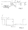
- Figure 1 shows a continuous switching power supply with its input terminals on which a voltage is applied input in slots, Ve, and, between the two input terminals, the primary of a transformer T, in series with a control circuit of cutting, A;
- the cutting control circuit is a circuit classic and, in the example described, this circuit comprises in association a MOTOROLA circuit bearing the reference SG3526 and a circuit current measurement; the SG3526 circuit performs a cutting, in the time, half-periods of the voltage Ve as a function of the value of the measured current.
- the transformer T has a mid-point secondary whose the midpoint is connected to ground and the two ends of which are respectively connected to the anodes of two diodes D1, D2. Cathodes of these two diodes are interconnected and coupled, through a filter low pass, at the first end of a load B of which the second end is connected to ground; the low pass filter has a inductance L connected between the point common to the diodes D1, D2, and a capacitor C mounted in parallel on the load B.
- the circuit of rectification consisting of the elements T, D1 and D2 provides a current, the, to the low-pass filter and this current which crosses the inductance L, is divided into two parts, one of which, lb, constitutes the current in the load B.
- the power supply is used to supply the energy required to amplify an image signal in television at French standard "L" standard. That is, in this example, the load B of Figure 1 is a variable load and that the current lb to it supply can be represented schematically, as a function of time, by the curve in strong lines of the graph of Figure 2, with weft tops of 160 ⁇ s and a frame period of 20ms.
- the current la in the inductance L has, for the rising edge of each white half-image, the shape indicated in broken lines at the start of one of these white half-images; these forms are given subject, in this representation, that the and lb, in the part of their course where they are parallel and apart one of the other are, in fact, confused.
- the shape of the current la is due to the presence of inductance L which delays the rise of current lb in the load B, and which therefore requires the current to reach it, at the start of half white image, a higher lc value than at steady state, lp.
- the ratio lc / lp is 1.3, the duration of the transient regime is 220 ⁇ s and the return, after transient regime, to normal steady state temperatures will take approximately 10 ms.
- the original part of the switching control circuit is that intended to supply a signal G of inhibition of switching, that is to say a signal which blocks the switching power supply bringing its output voltage to zero.
- This original part includes a voltage comparator 2 with, on one of its two inputs, a voltage preferably Vr supplied by a terminal of a voltage source whose other terminal is grounded. Between the other terminal of the comparator 2 and the ground is connected, an assembly made of a current source, 3, in parallel on a resistor r1.
- the current source is constituted by a rectifier assembly with a transformer comprising a primary in series with the primary of the transformer T of FIG.
- This new part comprises, a diode D whose anode is connected to the output of comparator 2, and whose cathode is coupled to ground by a resistor r3 and is connected to an input with inversion of an OR gate, 4.
- the OR gate, 4 has an output connected to the control input of a monostable flip-flop 5 whose duration of the quasi-stable state, 220 ⁇ s in the example described, is determined by the values of a resistance r5 connected between a first access of the flip-flop and a point with fixed potential Vp, and a capacitor C5 connected between the first access and a second access of flip-flop 5.
- the outputs Q and Q of the flip-flop 5 are respectively connected to a direct input and to an input with inversion of an OR gate, 6, the output of which is connected to the control input of a monostable flip-flop 7; the 10 ms that the quasi-stable state of flip-flop 7 lasts, in the example described, are determined by the values of a resistor r7 connected between a first access of flip-flop 7 and the point with fixed potential Vp, and a capacitor C7 connected between the first access and a second access of the flip-flop 7.
- the output Q of flip-flop 7 is connected to a direct input from the OR gate 4.
- the output Q of the monostable flip-flop 5 is also connected to the first common ends of two resistors r6, r8, the second ends of which are connected to ground for the resistor r8 and to the base of an npn transistor, Tr1, for the resistor r6.
- the transistor Tr1 has its emitter connected to ground and its collector connected to the gate of a MOSFET transistor, N channel, Tr2.
- the transistor Tr2 has its source connected to ground and its drain coupled by a resistor r2 to that of the ends of the resistor r1 which is not grounded.
- the role of the new part is to replace the resistor r1 alone with the resistors r1 and r2 in parallel for a time which will be specified later.
- the OR gate, 4 has its direct input at O, its input with inversion at 1 and therefore its output at 0.
- the outputs Q and Q of flip-flop 5 are therefore respectively at O and 1 which means that the output Q of flip-flop 7 is at O and, by the "logic 1" delivered in the form of a positive voltage by the output Q of flip-flop 5, the transistor Tr1 is on and the transistor Tr2 blocked. Only the resistor r1 is therefore connected to the current source 3.
- Monostable scales 5 and 7 are triggered by the front the transition from “logical O” to "logical 1" of the signal on their input ordered. So when K.la.r1 becomes greater than Vr the front of the switching from 1 to O of the comparator output practically triggers instantly the transition to the quasi-stable state of the two flip-flops 5 and 7. And, for a first duration given by the 220 ⁇ s of the quasi-stable state of flip-flop 5, the resistor r2 is connected in parallel to the resistance r1, thus bringing the output of comparator 2 to the value 1 of the less as long as K.la (r1.r2) / (r1 + r2) is less than Vr.
- the present invention is not limited to the example described and finds its application where it is asked to a feeding to cutting to provide, for very short moments, more power important than in normal operating conditions.
- the means to implement must authorize an overshoot of the normal operation but limiting it in amplitude, duration and maximum repetition frequency at acceptable values for food; such means can be designed in different ways manners of the art especially from delay lines and not of monostable scales; in the example described the amplitude was regulated by (r1.r2) / (r1 + r2), the duration was that of the quasi-stable state of the flip-flop 5 and the maximum repetition frequency was for the period duration of the quasi-stable state of the rocker 7.
Landscapes
- Engineering & Computer Science (AREA)
- Power Engineering (AREA)
- Dc-Dc Converters (AREA)
- Television Receiver Circuits (AREA)
- Emergency Protection Circuit Devices (AREA)
Description
- la figure 1, un schéma de principe d'une alimentation selon l'art connu,
- la figure 2, des signaux à obtenir
- la figure 3, un schéma détaillé qui montre comment modifier, selon l'invention, l'alimentation de la figure 1.
Tant que le produit K.la . r1 est inférieur à la tension de référence Vr, le comparateur 2 délivre un signal G = "1 logique" et le découpage peut s'effectuer normalement.
Claims (5)
- Alimentation continue à découpage comportant un circuit de redressement (T, D1, D2) pour fournir un premier courant (la), un filtre passe-bas (L, C) pour recevoir le premier courant et délivrer un second courant (lb) sur des bornes de sortie de l'alimentation, des moyens de commande comportant des moyens de comparaison (2, Vr, r1) pour surveiller le premier courant et, lorsque la valeur du premier courant est au moins égale à une valeur de référence (Vr/K.r1), délivrer un signal de blocage (G=0) pour bloquer le circuit de redressement, caractérisée par le fait qu'elle comporte un premier moyen (5) produisant un premier retard, branché à la sortie des moyens de comparaison et déclenché par le franchissement d'un premier seuil (Ip) par le premier courant (la), ce premier moyen commandant (Tr1, Tr2, un dispositif (2) augmentant ladite valeur de référence (Vr(r1+r2)/K.r1.r2), et par le fait qu'elle comporte un second moyen (7) produisant un second retard, relié au premier moyen de retard et inhibant celui-ci à la fin dudit premier retard.
- Alimentation selon la revendication 1, caractérisée par le fait que ladite valeur de référence est déterminée par une première résistance (r1) reliée à une entrée des moyens de comparaison et que le dispositif augmentant cette valeur de référence est une seconde résistance (r2) commutée en parallèle avec la première résistance sous l'effet du signal de sortie du premier moyen de retard.
- Alimentation selon la revendication 1 ou 2, caractérisée par le fait que les moyens de retard sont des bascules monostables.
- Alimentation selon la revendication 1 ou 2, caractérisée par le fait que les moyens de retard sont des lignes à retard.
- Alimentation selon l'une des revendications précédentes, caractérisée en ce que, étant destinée à fournir l'énergie nécessaire à l'amplification d'un signal image en télévision, elle est réglée avec une seconde durée inférieure à la durée d'une trame de télévision et une première durée de valeur très inférieure à la seconde durée.
Applications Claiming Priority (2)
| Application Number | Priority Date | Filing Date | Title |
|---|---|---|---|
| FR9606275 | 1996-05-21 | ||
| FR9606275A FR2749110B1 (fr) | 1996-05-21 | 1996-05-21 | Alimentation continue a decoupage, a limitation de courant |
Publications (2)
| Publication Number | Publication Date |
|---|---|
| EP0809348A1 EP0809348A1 (fr) | 1997-11-26 |
| EP0809348B1 true EP0809348B1 (fr) | 2002-07-31 |
Family
ID=9492306
Family Applications (1)
| Application Number | Title | Priority Date | Filing Date |
|---|---|---|---|
| EP19970401028 Expired - Lifetime EP0809348B1 (fr) | 1996-05-21 | 1997-05-07 | Alimentation continue à découpage, à limitation de courant |
Country Status (3)
| Country | Link |
|---|---|
| EP (1) | EP0809348B1 (fr) |
| DE (1) | DE69714345T2 (fr) |
| FR (1) | FR2749110B1 (fr) |
Family Cites Families (1)
| Publication number | Priority date | Publication date | Assignee | Title |
|---|---|---|---|---|
| US4811184A (en) * | 1988-05-10 | 1989-03-07 | General Electric Company | Switch-mode power supply with dynamic adjustment of current sense magnitude |
-
1996
- 1996-05-21 FR FR9606275A patent/FR2749110B1/fr not_active Expired - Fee Related
-
1997
- 1997-05-07 EP EP19970401028 patent/EP0809348B1/fr not_active Expired - Lifetime
- 1997-05-07 DE DE1997614345 patent/DE69714345T2/de not_active Expired - Lifetime
Also Published As
| Publication number | Publication date |
|---|---|
| FR2749110A1 (fr) | 1997-11-28 |
| DE69714345D1 (de) | 2002-09-05 |
| FR2749110B1 (fr) | 1998-08-14 |
| DE69714345T2 (de) | 2003-04-03 |
| EP0809348A1 (fr) | 1997-11-26 |
Similar Documents
| Publication | Publication Date | Title |
|---|---|---|
| EP0041883B1 (fr) | Dispositif d'alimentation à régulation par découpage, combiné au circuit de balayage-ligne d'un récepteur de télévision qu'il alimente | |
| EP1630961B1 (fr) | Dispositif de commande d'un transistor de puissance | |
| EP0002983A1 (fr) | Circuit de commande de puissance et alimentation à découpage l'utilisant | |
| EP0240434B1 (fr) | Circuit de protection d'alimentation à découpage | |
| EP0193435A1 (fr) | Circuit de commande d'alimentation à découpage à démarrage automatique | |
| EP0193436B1 (fr) | Circuit de commande d'alimentation à découpage à démarrage progressif | |
| FR2863118A1 (fr) | Circuit onduleur | |
| FR2519278A1 (fr) | Source electronique d'energie de soudage avec un comportement statique et dynamique pour le soudage a l'arc | |
| EP0815635B1 (fr) | Circuit d'alimentation a condensateur de stockage | |
| BE1012284A4 (fr) | Source d'alimentation a decoupage. | |
| EP0809348B1 (fr) | Alimentation continue à découpage, à limitation de courant | |
| FR2547133A1 (fr) | Circuit destine a prevenir une dissipation excessive d'energie dans les dispositifs commutateurs de puissance | |
| EP0022380B1 (fr) | Dispositif d'alimentation par découpage combiné avec un circuit de balayage-ligne d'un récepteur de télévision, régulé par déphasage variable | |
| EP0331592B1 (fr) | Dispositif de démarrage progressif d'une alimentation à découpage | |
| EP0265322B1 (fr) | Circuit de commande en mode veille d'une alimentation à découpage | |
| EP2230027A1 (fr) | Générateur pour transducteur piézoélectrique | |
| FR2494943A1 (fr) | Circuit d'effacement video avec allure controlee de deseffacement | |
| FR2559980A1 (fr) | Circuit de commutation des frequences pour dispositif de visualisation video a plusieurs frequences de balayage | |
| EP0021867B1 (fr) | Dispositif d'alimentation à découpage régulé contre les variations de tension d'entrée et de puissance de sortie, notamment pour récepteur de télévision | |
| EP0006785B1 (fr) | Dispositif de chauffage de cathode pour tube électronique de puissance, et émetteur comportant un tel dispositif | |
| FR2520958A1 (fr) | Circuit auxiliaire pour televiseur | |
| EP0080915B1 (fr) | Circuit de commande de balayage de récepteur de télévision, à démarrage progressif | |
| EP0108662A1 (fr) | Circuit de commande de base d'un transistor de puissance | |
| FR2577358A1 (fr) | Alimentation a decoupage protegee contre des surintensites tres fortes | |
| CH682019A5 (en) | Amplitude control circuit for oscillator circuit - includes current sources and current mirror in circuit to limit final output voltage of oscillator control circuit |
Legal Events
| Date | Code | Title | Description |
|---|---|---|---|
| PUAI | Public reference made under article 153(3) epc to a published international application that has entered the european phase |
Free format text: ORIGINAL CODE: 0009012 |
|
| AK | Designated contracting states |
Kind code of ref document: A1 Designated state(s): DE FR GB IT |
|
| 17P | Request for examination filed |
Effective date: 19980309 |
|
| 17Q | First examination report despatched |
Effective date: 19990325 |
|
| GRAG | Despatch of communication of intention to grant |
Free format text: ORIGINAL CODE: EPIDOS AGRA |
|
| RAP1 | Party data changed (applicant data changed or rights of an application transferred) |
Owner name: THALES |
|
| GRAG | Despatch of communication of intention to grant |
Free format text: ORIGINAL CODE: EPIDOS AGRA |
|
| GRAH | Despatch of communication of intention to grant a patent |
Free format text: ORIGINAL CODE: EPIDOS IGRA |
|
| GRAH | Despatch of communication of intention to grant a patent |
Free format text: ORIGINAL CODE: EPIDOS IGRA |
|
| GRAA | (expected) grant |
Free format text: ORIGINAL CODE: 0009210 |
|
| AK | Designated contracting states |
Kind code of ref document: B1 Designated state(s): DE FR GB IT |
|
| REG | Reference to a national code |
Ref country code: GB Ref legal event code: FG4D Free format text: NOT ENGLISH |
|
| REF | Corresponds to: |
Ref document number: 69714345 Country of ref document: DE Date of ref document: 20020905 |
|
| GBT | Gb: translation of ep patent filed (gb section 77(6)(a)/1977) |
Effective date: 20021004 |
|
| PLBE | No opposition filed within time limit |
Free format text: ORIGINAL CODE: 0009261 |
|
| STAA | Information on the status of an ep patent application or granted ep patent |
Free format text: STATUS: NO OPPOSITION FILED WITHIN TIME LIMIT |
|
| 26N | No opposition filed |
Effective date: 20030506 |
|
| PGFP | Annual fee paid to national office [announced via postgrant information from national office to epo] |
Ref country code: IT Payment date: 20070507 Year of fee payment: 11 |
|
| PG25 | Lapsed in a contracting state [announced via postgrant information from national office to epo] |
Ref country code: IT Free format text: LAPSE BECAUSE OF NON-PAYMENT OF DUE FEES Effective date: 20080507 |
|
| REG | Reference to a national code |
Ref country code: DE Ref legal event code: R082 Ref document number: 69714345 Country of ref document: DE Representative=s name: DREISS PATENTANWAELTE, DE |
|
| REG | Reference to a national code |
Ref country code: DE Ref legal event code: R082 Ref document number: 69714345 Country of ref document: DE Representative=s name: DREISS PATENTANWAELTE, DE |
|
| REG | Reference to a national code |
Ref country code: DE Ref legal event code: R082 Ref document number: 69714345 Country of ref document: DE Representative=s name: DREISS PATENTANWAELTE PARTG MBB, DE Effective date: 20110923 |
|
| REG | Reference to a national code |
Ref country code: GB Ref legal event code: 732E Free format text: REGISTERED BETWEEN 20120705 AND 20120711 |
|
| PGFP | Annual fee paid to national office [announced via postgrant information from national office to epo] |
Ref country code: GB Payment date: 20120531 Year of fee payment: 16 |
|
| REG | Reference to a national code |
Ref country code: FR Ref legal event code: TP Owner name: PL TECHNOLOGIES AG, CH Effective date: 20121207 |
|
| GBPC | Gb: european patent ceased through non-payment of renewal fee |
Effective date: 20130507 |
|
| PGFP | Annual fee paid to national office [announced via postgrant information from national office to epo] |
Ref country code: DE Payment date: 20131128 Year of fee payment: 17 |
|
| PGFP | Annual fee paid to national office [announced via postgrant information from national office to epo] |
Ref country code: FR Payment date: 20131128 Year of fee payment: 17 |
|
| PG25 | Lapsed in a contracting state [announced via postgrant information from national office to epo] |
Ref country code: GB Free format text: LAPSE BECAUSE OF NON-PAYMENT OF DUE FEES Effective date: 20130507 |
|
| REG | Reference to a national code |
Ref country code: DE Ref legal event code: R119 Ref document number: 69714345 Country of ref document: DE |
|
| REG | Reference to a national code |
Ref country code: DE Ref legal event code: R119 Ref document number: 69714345 Country of ref document: DE Effective date: 20141202 |
|
| REG | Reference to a national code |
Ref country code: FR Ref legal event code: ST Effective date: 20150130 |
|
| PG25 | Lapsed in a contracting state [announced via postgrant information from national office to epo] |
Ref country code: DE Free format text: LAPSE BECAUSE OF NON-PAYMENT OF DUE FEES Effective date: 20141202 |
|
| PG25 | Lapsed in a contracting state [announced via postgrant information from national office to epo] |
Ref country code: FR Free format text: LAPSE BECAUSE OF NON-PAYMENT OF DUE FEES Effective date: 20140602 |