EP0809348B1 - DC voltage switching power supply with current limitation - Google Patents
DC voltage switching power supply with current limitation Download PDFInfo
- Publication number
- EP0809348B1 EP0809348B1 EP19970401028 EP97401028A EP0809348B1 EP 0809348 B1 EP0809348 B1 EP 0809348B1 EP 19970401028 EP19970401028 EP 19970401028 EP 97401028 A EP97401028 A EP 97401028A EP 0809348 B1 EP0809348 B1 EP 0809348B1
- Authority
- EP
- European Patent Office
- Prior art keywords
- current
- power supply
- delay
- duration
- resistor
- Prior art date
- Legal status (The legal status is an assumption and is not a legal conclusion. Google has not performed a legal analysis and makes no representation as to the accuracy of the status listed.)
- Expired - Lifetime
Links
Images

Classifications
-
- H—ELECTRICITY
- H02—GENERATION; CONVERSION OR DISTRIBUTION OF ELECTRIC POWER
- H02M—APPARATUS FOR CONVERSION BETWEEN AC AND AC, BETWEEN AC AND DC, OR BETWEEN DC AND DC, AND FOR USE WITH MAINS OR SIMILAR POWER SUPPLY SYSTEMS; CONVERSION OF DC OR AC INPUT POWER INTO SURGE OUTPUT POWER; CONTROL OR REGULATION THEREOF
- H02M1/00—Details of apparatus for conversion
- H02M1/32—Means for protecting converters other than automatic disconnection
-
- H—ELECTRICITY
- H02—GENERATION; CONVERSION OR DISTRIBUTION OF ELECTRIC POWER
- H02M—APPARATUS FOR CONVERSION BETWEEN AC AND AC, BETWEEN AC AND DC, OR BETWEEN DC AND DC, AND FOR USE WITH MAINS OR SIMILAR POWER SUPPLY SYSTEMS; CONVERSION OF DC OR AC INPUT POWER INTO SURGE OUTPUT POWER; CONTROL OR REGULATION THEREOF
- H02M3/00—Conversion of DC power input into DC power output
- H02M3/22—Conversion of DC power input into DC power output with intermediate conversion into AC
- H02M3/24—Conversion of DC power input into DC power output with intermediate conversion into AC by static converters
- H02M3/28—Conversion of DC power input into DC power output with intermediate conversion into AC by static converters using discharge tubes with control electrode or semiconductor devices with control electrode to produce the intermediate AC
- H02M3/325—Conversion of DC power input into DC power output with intermediate conversion into AC by static converters using discharge tubes with control electrode or semiconductor devices with control electrode to produce the intermediate AC using devices of a triode or a transistor type requiring continuous application of a control signal
- H02M3/335—Conversion of DC power input into DC power output with intermediate conversion into AC by static converters using discharge tubes with control electrode or semiconductor devices with control electrode to produce the intermediate AC using devices of a triode or a transistor type requiring continuous application of a control signal using semiconductor devices only
- H02M3/33507—Conversion of DC power input into DC power output with intermediate conversion into AC by static converters using discharge tubes with control electrode or semiconductor devices with control electrode to produce the intermediate AC using devices of a triode or a transistor type requiring continuous application of a control signal using semiconductor devices only with automatic control of the output voltage or current, e.g. flyback converters
Definitions
- the present invention relates to the field of power supplies switching power supplies and in particular switching power supplies, current limitation, used with a load whose value may vary; it also relates to the protection of such power supplies against short circuits.
- the object of the present invention is to avoid or, at the very least, to reduce this drawback in the case of continuous power supplies at cutting.
- the present invention relates to power supplies such as described in the claims.
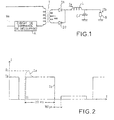
- Figure 1 shows a continuous switching power supply with its input terminals on which a voltage is applied input in slots, Ve, and, between the two input terminals, the primary of a transformer T, in series with a control circuit of cutting, A;
- the cutting control circuit is a circuit classic and, in the example described, this circuit comprises in association a MOTOROLA circuit bearing the reference SG3526 and a circuit current measurement; the SG3526 circuit performs a cutting, in the time, half-periods of the voltage Ve as a function of the value of the measured current.
- the transformer T has a mid-point secondary whose the midpoint is connected to ground and the two ends of which are respectively connected to the anodes of two diodes D1, D2. Cathodes of these two diodes are interconnected and coupled, through a filter low pass, at the first end of a load B of which the second end is connected to ground; the low pass filter has a inductance L connected between the point common to the diodes D1, D2, and a capacitor C mounted in parallel on the load B.
- the circuit of rectification consisting of the elements T, D1 and D2 provides a current, the, to the low-pass filter and this current which crosses the inductance L, is divided into two parts, one of which, lb, constitutes the current in the load B.
- the power supply is used to supply the energy required to amplify an image signal in television at French standard "L" standard. That is, in this example, the load B of Figure 1 is a variable load and that the current lb to it supply can be represented schematically, as a function of time, by the curve in strong lines of the graph of Figure 2, with weft tops of 160 ⁇ s and a frame period of 20ms.
- the current la in the inductance L has, for the rising edge of each white half-image, the shape indicated in broken lines at the start of one of these white half-images; these forms are given subject, in this representation, that the and lb, in the part of their course where they are parallel and apart one of the other are, in fact, confused.
- the shape of the current la is due to the presence of inductance L which delays the rise of current lb in the load B, and which therefore requires the current to reach it, at the start of half white image, a higher lc value than at steady state, lp.
- the ratio lc / lp is 1.3, the duration of the transient regime is 220 ⁇ s and the return, after transient regime, to normal steady state temperatures will take approximately 10 ms.
- the original part of the switching control circuit is that intended to supply a signal G of inhibition of switching, that is to say a signal which blocks the switching power supply bringing its output voltage to zero.
- This original part includes a voltage comparator 2 with, on one of its two inputs, a voltage preferably Vr supplied by a terminal of a voltage source whose other terminal is grounded. Between the other terminal of the comparator 2 and the ground is connected, an assembly made of a current source, 3, in parallel on a resistor r1.
- the current source is constituted by a rectifier assembly with a transformer comprising a primary in series with the primary of the transformer T of FIG.
- This new part comprises, a diode D whose anode is connected to the output of comparator 2, and whose cathode is coupled to ground by a resistor r3 and is connected to an input with inversion of an OR gate, 4.
- the OR gate, 4 has an output connected to the control input of a monostable flip-flop 5 whose duration of the quasi-stable state, 220 ⁇ s in the example described, is determined by the values of a resistance r5 connected between a first access of the flip-flop and a point with fixed potential Vp, and a capacitor C5 connected between the first access and a second access of flip-flop 5.
- the outputs Q and Q of the flip-flop 5 are respectively connected to a direct input and to an input with inversion of an OR gate, 6, the output of which is connected to the control input of a monostable flip-flop 7; the 10 ms that the quasi-stable state of flip-flop 7 lasts, in the example described, are determined by the values of a resistor r7 connected between a first access of flip-flop 7 and the point with fixed potential Vp, and a capacitor C7 connected between the first access and a second access of the flip-flop 7.
- the output Q of flip-flop 7 is connected to a direct input from the OR gate 4.
- the output Q of the monostable flip-flop 5 is also connected to the first common ends of two resistors r6, r8, the second ends of which are connected to ground for the resistor r8 and to the base of an npn transistor, Tr1, for the resistor r6.
- the transistor Tr1 has its emitter connected to ground and its collector connected to the gate of a MOSFET transistor, N channel, Tr2.
- the transistor Tr2 has its source connected to ground and its drain coupled by a resistor r2 to that of the ends of the resistor r1 which is not grounded.
- the role of the new part is to replace the resistor r1 alone with the resistors r1 and r2 in parallel for a time which will be specified later.
- the OR gate, 4 has its direct input at O, its input with inversion at 1 and therefore its output at 0.
- the outputs Q and Q of flip-flop 5 are therefore respectively at O and 1 which means that the output Q of flip-flop 7 is at O and, by the "logic 1" delivered in the form of a positive voltage by the output Q of flip-flop 5, the transistor Tr1 is on and the transistor Tr2 blocked. Only the resistor r1 is therefore connected to the current source 3.
- Monostable scales 5 and 7 are triggered by the front the transition from “logical O” to "logical 1" of the signal on their input ordered. So when K.la.r1 becomes greater than Vr the front of the switching from 1 to O of the comparator output practically triggers instantly the transition to the quasi-stable state of the two flip-flops 5 and 7. And, for a first duration given by the 220 ⁇ s of the quasi-stable state of flip-flop 5, the resistor r2 is connected in parallel to the resistance r1, thus bringing the output of comparator 2 to the value 1 of the less as long as K.la (r1.r2) / (r1 + r2) is less than Vr.
- the present invention is not limited to the example described and finds its application where it is asked to a feeding to cutting to provide, for very short moments, more power important than in normal operating conditions.
- the means to implement must authorize an overshoot of the normal operation but limiting it in amplitude, duration and maximum repetition frequency at acceptable values for food; such means can be designed in different ways manners of the art especially from delay lines and not of monostable scales; in the example described the amplitude was regulated by (r1.r2) / (r1 + r2), the duration was that of the quasi-stable state of the flip-flop 5 and the maximum repetition frequency was for the period duration of the quasi-stable state of the rocker 7.
Landscapes
- Engineering & Computer Science (AREA)
- Power Engineering (AREA)
- Dc-Dc Converters (AREA)
- Television Receiver Circuits (AREA)
- Emergency Protection Circuit Devices (AREA)
Description
La présente invention concerne le domaine des alimentations continues à découpage et en particulier des alimentations à découpage, à limitation de courant, utilisées avec une charge dont la valeur peut varier ; elle concerne également la protection de telles alimentations contre les courts-circuits.The present invention relates to the field of power supplies switching power supplies and in particular switching power supplies, current limitation, used with a load whose value may vary; it also relates to the protection of such power supplies against short circuits.
Lorsque l'énergie fournie par une alimentation doit pouvoir atteindre une valeur de crête donnée, il est classique de dimensionner cette alimentation de telle sorte que sa puissance nominale, généralement définie à 1 dB de compression, corresponde à cette valeur de crête.When the energy supplied by a food must be able to reach a given peak value, it is conventional to size this power supply so that its nominal power, generally defined at 1 dB compression, corresponds to this peak value.
Lorsque cette valeur de crête n'est atteinte que pendant des instants très courts et que, pendant le reste du temps de fonctionnement, l'alimentation n'a à fournir qu'une énergie relativement plus faible, il est frustrant et coûteux de devoir employer, du fait de ces très courts instants de fonctionnement à forte puissance, une alimentation sur-dimensionnée en régime normal.When this peak value is reached only for instants very short and that, during the rest of the operating time, food only has to provide relatively lower energy it is frustrating and costly to have to employ, due to these very short moments of high power operation, oversized power supply normal diet.
On connaít d'après le document US-A-4 811 184 un dispositif de limitation de courant pour alimentation à découpage nécessitant pour son fonctionnement des signaux extérieurs de synchronisation.We know from document US-A-4 811 184 a device for current limitation for switching power supply requiring for its operation of external synchronization signals.
Le but de la présente invention est d'éviter ou, pour le moins, de réduire cet inconvénient dans le cas des alimentations continues à découpage.The object of the present invention is to avoid or, at the very least, to reduce this drawback in the case of continuous power supplies at cutting.
Pour y parvenir il est proposé d'autoriser l'utilisation de l'alimentation au-dessus de sa puissance nominale pendant de très brefs instants, de séparer ces très brefs instants par des intervalles de temps pendant lesquels l'alimentation est utilisée, au plus, à sa puissance nominale et d'assortir ce fonctionnement de conditions : - limitation, pendant les très brefs instants, de la puissance disponible à une valeur telle que, même si des composants de l'alimentation atteignent des températures relativement élevées, ils ne soient pas détériorés - durée des intervalles de temps suffisante pour permettre aux composants qui ont atteint une température relativement élevée, de revenir à une température normale de fonctionnement.To achieve this, it is proposed to authorize the use of food above its nominal power for very short moments, separate these very brief moments by time intervals during which the power supply is used, at most, at its nominal power and to attach conditions to this operation: - limitation, during very brief moments, of the power available at a value such that, even if food components reach relatively high temperatures high, they are not deteriorated - length of time intervals sufficient to allow components that have reached a temperature relatively high, to return to a normal temperature of operation.
La présente invention a pour objet des alimentations telles que décrites dans les revendications. The present invention relates to power supplies such as described in the claims.
Il est à noter que selon le brevet US-A-4 811 184 il est proposé, avec une alimentation à découpage, d'autoriser une surcharge en courant de très courte durée par rapport au régime normal de fonctionnements ; mais dans ce document, l'autorisation de surcharge est donnée à partir d'un signal de synchronisation extérieur, prédéfini en fonction de la variation de charge. It should be noted that according to US-A-4,811,184 it is proposed, with a switching power supply, to allow an overload in current of very short duration compared to the normal regime of operations; but in this document, the authorization of overload is given from an external synchronization signal, preset according to the load variation.
La présente invention décrite à l'aide de la description ci-après et des figures s'y rapportant qui représentent :
- la figure 1, un schéma de principe d'une alimentation selon l'art connu,
- la figure 2, des signaux à obtenir
- la figure 3, un schéma détaillé qui montre comment modifier, selon l'invention, l'alimentation de la figure 1.
- FIG. 1, a block diagram of a power supply according to the known art,
- Figure 2, signals to obtain
- FIG. 3, a detailed diagram which shows how to modify, according to the invention, the power supply of FIG. 1.
La figure 1 représente une alimentation continue à découpage avec ses bornes d'entrée sur lesquelles est appliquée une tension d'entrée en créneaux, Ve, et, entre les deux bornes d'entrée, le primaire d'un transformateur T, en série avec un circuit de commande de découpage, A ; le circuit de commande de découpage est un circuit classique et, dans l'exemple décrit, ce circuit comporte en association un circuit MOTOROLA portant la référence SG3526 et un circuit de mesure de courant ; le circuit SG3526 réalise un découpage, dans le temps, des demi-périodes de la tension Ve en fonction de la valeur du courant mesuré.Figure 1 shows a continuous switching power supply with its input terminals on which a voltage is applied input in slots, Ve, and, between the two input terminals, the primary of a transformer T, in series with a control circuit of cutting, A; the cutting control circuit is a circuit classic and, in the example described, this circuit comprises in association a MOTOROLA circuit bearing the reference SG3526 and a circuit current measurement; the SG3526 circuit performs a cutting, in the time, half-periods of the voltage Ve as a function of the value of the measured current.
Le transformateur T comporte un secondaire à point milieu dont le point milieu est relié à la masse et dont les deux extrémités sont respectivement reliées aux anodes de deux diodes D1, D2. Les cathodes de ces deux diodes sont reliées entre elles et couplées, à travers un filtre passe-bas, à la première extrémité d'une charge B dont la seconde extrémité est reliée à la masse ; le filtre passe-bas comporte une inductance L branchée entre le point commun aux diodes D1, D2, et un condensateur C monté en parallèle sur la charge B. Le circuit de redressement constitué des éléments T, D1 et D2, fournit un courant, la, au filtre passe-bas et ce courant qui traverse l'inductance L, se divise en deux parties dont l'une, lb, constitue le courant dans la charge B.The transformer T has a mid-point secondary whose the midpoint is connected to ground and the two ends of which are respectively connected to the anodes of two diodes D1, D2. Cathodes of these two diodes are interconnected and coupled, through a filter low pass, at the first end of a load B of which the second end is connected to ground; the low pass filter has a inductance L connected between the point common to the diodes D1, D2, and a capacitor C mounted in parallel on the load B. The circuit of rectification consisting of the elements T, D1 and D2, provides a current, the, to the low-pass filter and this current which crosses the inductance L, is divided into two parts, one of which, lb, constitutes the current in the load B.
Dans le cas de l'exemple décrit l'alimentation sert à fournir l'énergie nécessaire à l'amplification d'un signal image en télévision au standard français norme "L". C'est-à-dire que, dans cet exemple, la charge B de la figure 1 est une charge variable et que le courant lb à lui fournir peut être représenté schématiquement, en fonction du temps, par la courbe en traits forts du graphique de la figure 2, avec des tops trame de 160µs et une période trame de 20ms. Pour obtenir un tel courant lb dans la charge il faut que le courant la dans l'inductance L ait, pour le flanc de montée de chaque demi-image blanche, la forme indiquée en traits interrompus au début de l'une de ces demi-images blanches ; ces formes sont données sous réserve, dans cette représentation, que la et lb, dans la partie de leur tracé où ils sont parallèles et écartés l'un de l'autre sont, en fait, confondus. La forme du courant la est due à la présence de l'inductance L qui retarde la montée du courant lb dans la charge B, et qui nécessite donc que le courant la atteigne, en début de demi-image blanche, une valeur lc plus élevée qu'en régime établi, lp.In the case of the example described, the power supply is used to supply the energy required to amplify an image signal in television at French standard "L" standard. That is, in this example, the load B of Figure 1 is a variable load and that the current lb to it supply can be represented schematically, as a function of time, by the curve in strong lines of the graph of Figure 2, with weft tops of 160µs and a frame period of 20ms. To obtain such a current lb in the load it is necessary that the current la in the inductance L has, for the rising edge of each white half-image, the shape indicated in broken lines at the start of one of these white half-images; these forms are given subject, in this representation, that the and lb, in the part of their course where they are parallel and apart one of the other are, in fact, confused. The shape of the current la is due to the presence of inductance L which delays the rise of current lb in the load B, and which therefore requires the current to reach it, at the start of half white image, a higher lc value than at steady state, lp.
Or le dépassement de la valeur lp, pour atteindre la valeur lc puis revenir à la valeur lp, ne dure qu'une infime fraction du temps d'une demi-image blanche. Il est donc possible d'accepter que, pendant ce régime transitoire au cours duquel l'alimentation fournit un courant la supérieur à la valeur lp, certains des composants atteignent des températures supérieures à celles qu'ils peuvent atteindre lors d'un fonctionnement en régime établi ; un tel fonctionnement est acceptable sous réserve que deux conditions soient remplies afin d'éviter une détérioration du matériel : - les températures atteintes en régime transitoire doivent pouvoir être supportées sans dommages, par les composants concernés, jusqu'au retour à des températures de régime établi, - le retour à des températures normales de fonctionnement en régime établi doit se faire, en tout état de cause, au plus tard en fin de trame pour les cas de deux demi-images blanches consécutives.Or exceeding the value lp, to reach the value lc then return to lp value, lasts only a tiny fraction of the time of a white half-image. It is therefore possible to accept that, during this transient state during which the supply provides a current the greater than the lp value, some of the components reach temperatures higher than they can reach during a steady state operation; such operation is acceptable provided that two conditions are met in order to avoid a deterioration of the equipment: - the temperatures reached in regime transient must be able to be supported without damage, by the components concerned, until return to operating temperatures established, - return to normal operating temperatures in established regime must be done, in any event, at the latest at the end of frame for cases of two consecutive white half-images.
En fait il s'agit de réaliser un compromis entre différentes valeurs: celle du courant lp qui doit permettre un retour à la température de régime établi, celle du courant lc et de la durée du régime transitoire qui sont liées pour obtenir le courant lb tel que désiré en début de demi-image blanche, et celle du temps à ne pas dépasser pour revenir à des températures normales de fonctionnement en régime établi ; et ces valeurs sont à choisir en fonction de ceux des composants de l'alimentation qui sont les plus susceptibles de chauffer en régime transitoire, c'est-à-dire lors du dépassement du courant lp. En règle général le courant lp ne sera pris que légèrement inférieur au courant maximum à ne pas dépasser en régime établi. Quant aux valeurs du courant lc, de la durée du régime transitoire et du temps nécessaire pour le retour à des températures normales de fonctionnement, les deux premières déterminant la troisième, il s'agit de les choisir, de préférence, pour une utilisation optimum de l'alimentation, à savoir une utilisation aussi proche que possible de ses possibilités lors d'un fonctionnement en régime établi, ce régime établi étant à considérer lors d'une demi-image blanche.In fact it is a question of achieving a compromise between different values: that of the current lp which should allow a return to the established operating temperature, that of the current lc and the duration of the transient regime which are linked to obtain the current lb as desired at the beginning of the white half-image, and that of the time not to be exceeded to return to normal operating temperature established ; and these values are to be chosen according to those of the components of food that are most likely to heat up transient, that is to say when the current lp is exceeded. In good standing general the current lp will be taken only slightly lower than the current maximum not to be exceeded in steady state. As for the values of current lc, the duration of the transient state and the time necessary for return to normal operating temperatures, both first determining the third, it is a question of choosing them, preferably, for optimum use of the food, namely use as close as possible to its possibilities during operation in established regime, this established regime being to be considered during a half-image white.
Dans l'exemple décrit le rapport lc/lp vaut 1,3 , la durée du régime transitoire est de 220 µs et le retour, après régime transitoire, à des températures normales de régime établi se fait environ en 10 ms.In the example described the ratio lc / lp is 1.3, the duration of the transient regime is 220 µs and the return, after transient regime, to normal steady state temperatures will take approximately 10 ms.
Le problème est donc, avec une alimentation à découpage qui comporte déjà un premier seuil de limitation de courant qui détermine la valeur lp selon la figure 2, de munir cette alimentation d'un second seuil de limitation supérieur au premier, ne pouvant être atteint que pendant une durée brève devant la durée d'une trame et qui ne doit pas pouvoir être utilisé plus d'une fois par trame afin d'éviter les risques d'échauffement lors d'une utilisation anormale de l'alimentation.So the problem is, with a switching power supply that already has a first current limitation threshold which determines the lp value according to FIG. 2, to provide this supply with a second threshold limitation higher than the first, can only be reached during a short duration before the duration of a frame and which should not be able be used more than once per frame to avoid risks overheating during abnormal use of the power supply.
Une solution à ce problème est proposée, dans l'exemple décrit, par la modification, selon la figure 3, du circuit A de la figure 1.A solution to this problem is proposed, in the example described, by modifying, according to FIG. 3, circuit A of FIG. 1.
Sur la figure 3, à gauche d'une ligne verticale en traits interrompus, sont dessinés les seuls éléments du circuit de commande de découpage classique, d'origine, nécessaires à la compréhension de l'invention ; à droite de cette ligne ont été représentés les éléments ajoutés pour déterminer le second seuil de limitation.In Figure 3, to the left of a vertical line in lines interrupted, the only elements of the control circuit are drawn classic cutting, original, necessary for the understanding of the invention; to the right of this line have been represented the elements added to determine the second limitation threshold.
La partie d'origine du circuit de commande de découpage est
celle destinée à fournir un signal G d'inhibition du découpage, c'est-à-dire
un signal qui bloque l'alimentation à découpage amenant à zéro sa
tension de sortie. Cette partie d'origine comporte un comparateur de
tensions 2 avec, sur l'une de ses deux entrées, une tension de préférence
Vr fournie par une borne d'une source de tension dont l'autre borne est
à la masse. Entre l'autre borne du comparateur 2 et la masse est
branché un montage fait d'une source de courant, 3, en parallèle sur une
résistance r1. La source de courant est constituée par un montage
redresseur avec un transformateur comportant un primaire en série avec
le primaire du transformateur T de la figure 1 et un secondaire à point
milieu relié à la masse et associé à deux diodes de redressement comme
le secondaire du transformateur T et les diodes D1, D2 de la figure 1 ;
un tel montage redresseur, là où il est placé, fournit à la résistance r1 un
courant K.la, identique, à un coefficient de proportionnalité K près, au
courant la dans l'inductance L de la figure 1.
Tant que le produit K.la . r1 est inférieur à la tension de référence Vr, le
comparateur 2 délivre un signal G = "1 logique" et le découpage peut
s'effectuer normalement.The original part of the switching control circuit is that intended to supply a signal G of inhibition of switching, that is to say a signal which blocks the switching power supply bringing its output voltage to zero. This original part includes a
As long as the product K.la. r1 is less than the reference voltage Vr, the
Si le produit K.la . r1 devient supérieur à la tension de référence
Vr le comparateur 2 délivre un signal G = "O logique". Dans un circuit
de commande de découpage classique, c'est-à-dire sans la partie
nouvelle constituée par le montage électronique représenté sur la figure
3, à droite de la ligne verticale en traits interrompus, le découpage est
alors arrêté pour la demi-période en cours de la tension d'entrée de
l'alimentation.If the product K.la. r1 becomes greater than the reference voltage
Vr the
Dans ce qui suit il va maintenant être question de ce qui se passe quand, au circuit de commande de découpage classique, est ajoutée la partie nouvelle représentée sur la figure 3 à droite de la ligne verticale en traits interrompus.In what follows there will now be a question of what is passes when, at the conventional switching control circuit, is added the new part represented on figure 3 on the right of the line vertical in broken lines.
Cette partie nouvelle comporte, une diode D dont l'anode est
reliée à la sortie du comparateur 2, et dont la cathode est couplée à la
masse par une résistance r3 et est reliée à une entrée avec inversion
d'une porte OU,4. La porte OU,4, a une sortie reliée à l'entrée de
commande d'une bascule monostable 5 dont la durée de l'état quasi-stable,
220 µs dans l'exemple décrit, est déterminée par les valeurs
d'une résistance r5 branchée entre un premier accès de la bascule et un
point à potentiel fixe Vp, et d'un condensateur C5 branché entre le
premier accès et un second accès de la bascule 5. Les sorties Q et
La partie nouvelle a pour rôle de remplacer la résistance r1 seule
par les résistances r1 et r2 en parallèle pendant un temps qui sera
précisé plus loin. Ce remplacement de r1 par r1 et r2 en parallèle fait
que le courant qui déclenche le signal G = "1 logique" et donc l'arrêt du
découpage, est augmenté dans le rapport 1 + (r1/r2) puisque, avec r1
seul, le déclenchement se fait pour
Avec la partie nouvelle, tant que le courant la est suffisamment
faible pour ne pas faire passer le comparateur 2 de la valeur "1 logique"
à la valeur "O logique", la porte OU,4, a son entrée directe à O, son
entrée avec inversion à 1 et donc sa sortie à 0. Les sorties Q et
Les bascules monostables 5 et 7 sont déclenchées par le front
du passage du "O logique" au "1 logique" du signal sur leur entrée de
commande. Ainsi lorsque K.la.r1 devient supérieur à Vr le front du
passage de 1 à O de la sortie du comparateur déclenche pratiquement
instantanément le passage à l'état quasi-stable des deux bascules 5 et
7. Et, pendant une première durée donnée par les 220 µs de l'état quasi-stable
de la bascule 5, la résistance r2 est branchée en parallèle sur la
résistance r1, ramenant donc la sortie du comparateur 2 à la valeur 1 du
moins tant que K.la(r1.r2)/(r1 +r2) est inférieur à Vr. De plus, pendant
les 10 ms de l'état quasi-stable de la bascule 7, le "1 logique" appliqué
par cette bascule sur l'entrée directe de la porte 4, maintient la sortie de
cette porte au "1 logique" empêchant ainsi qu'un nouveau changement
de 1 à 0 de la sortie du comparateur 2 puisse autoriser, par un front de
0 à 1 sur l'entrée de commande de la bascule 5, un nouveau
branchement pendant 220 µs de la résistance r2 sur la résistance r1.
Ceci revient à dire que, à la suite de la première durée de 220µs, les
moyens, comportant en particulier les éléments 4, 5, Tr1, Tr2, r1, qui
ont permis le dépassement, sont inhibés par des moyens comportant en
particulier les éléments 6 et 7 ; cette seconde durée, comptée à partir de
la fin de l'autorisation de dépassement, c'est-à-dire après la fin de la
première durée, vaut 10 ms-220 µs dans l'exemple décrit.
La présente invention n'est pas limitée à l'exemple décrit et
trouve son application là où il est demandé à une alimentation à
découpage de fournir, pendant de très brefs instants, une puissance plus
importante qu'en régime normal de fonctionnement. Les moyens à
mettre en oeuvre doivent autoriser un dépassement du régime normal de
fonctionnement mais en le limitant en amplitude, en durée et en
fréquence maximale de répétition à des valeurs acceptables pour
l'alimentation ; de tels moyens peuvent être conçus de différentes
manières par l'homme du métier en particulier à partir de lignes à retard
et non de bascules monostables ; dans l'exemple décrit l'amplitude était
réglée par (r1.r2)/(r1 +r2), la durée était celle de l'état quasi-stable de la
bascule 5 et la fréquence de répétition maximale avait pour période la
durée de l'état quasi-stable de la bascule 7.The present invention is not limited to the example described and
finds its application where it is asked to a feeding to
cutting to provide, for very short moments, more power
important than in normal operating conditions. The means to
implement must authorize an overshoot of the normal
operation but limiting it in amplitude, duration and
maximum repetition frequency at acceptable values for
food; such means can be designed in different ways
manners of the art especially from delay lines
and not of monostable scales; in the example described the amplitude was
regulated by (r1.r2) / (r1 + r2), the duration was that of the quasi-stable state of the
flip-
Claims (5)
- Chopped DC power supply comprising a rectifying circuit (T, D1, D2) for providing a first current (Ia), a low-pass filter (L, C) for receiving the first current and delivering a second current (Ib) on output terminals of the power supply, control means comprising comparison means (2, Vr, r1) for monitoring the first current and, when the value of the first current is at least equal to a reference value (Vr/K.r1), delivering a turn-off signal (G=0) for turning off the rectifying circuit, characterized in that it comprises a first means (5) producing a first delay, connected to the output of the comparison means and triggered by the crossing of a first threshold (Ip) by the first current (Ia), this first means controlling (Tr1, Tr2) a device (2) increasing the said reference value (Vr(r1+r2)/K.r1.r2), and in that it comprises a second means (7) producing a second delay, linked to the first means of delay and disabling the latter at the end of the said first delay.
- Power supply according to Claim 1, characterized in that the said reference value is determined by a first resistor (r1) linked to an input of the comparison means and that the device increasing this reference value is a second resistor (r2) switched in parallel with the first resistor under the effect of the output signal from the first means of delay.
- Power supply according to Claim 1 or 2, characterized in that the means of delay are monostable flip-flops.
- Power supply according to Claim 1 or 2, characterized in that the means of delay are delay lines.
- Power supply according to one of the preceding claims, characterized in that, being intended to provide the energy required for the amplification of a television picture signal, it is adjusted with a second duration less than the duration of a television frame and a first duration of much lesser value than the second duration.
Applications Claiming Priority (2)
| Application Number | Priority Date | Filing Date | Title |
|---|---|---|---|
| FR9606275 | 1996-05-21 | ||
| FR9606275A FR2749110B1 (en) | 1996-05-21 | 1996-05-21 | CONTINUOUS POWER SUPPLY WITH CURRENT LIMITATION |
Publications (2)
| Publication Number | Publication Date |
|---|---|
| EP0809348A1 EP0809348A1 (en) | 1997-11-26 |
| EP0809348B1 true EP0809348B1 (en) | 2002-07-31 |
Family
ID=9492306
Family Applications (1)
| Application Number | Title | Priority Date | Filing Date |
|---|---|---|---|
| EP19970401028 Expired - Lifetime EP0809348B1 (en) | 1996-05-21 | 1997-05-07 | DC voltage switching power supply with current limitation |
Country Status (3)
| Country | Link |
|---|---|
| EP (1) | EP0809348B1 (en) |
| DE (1) | DE69714345T2 (en) |
| FR (1) | FR2749110B1 (en) |
Family Cites Families (1)
| Publication number | Priority date | Publication date | Assignee | Title |
|---|---|---|---|---|
| US4811184A (en) * | 1988-05-10 | 1989-03-07 | General Electric Company | Switch-mode power supply with dynamic adjustment of current sense magnitude |
-
1996
- 1996-05-21 FR FR9606275A patent/FR2749110B1/en not_active Expired - Fee Related
-
1997
- 1997-05-07 EP EP19970401028 patent/EP0809348B1/en not_active Expired - Lifetime
- 1997-05-07 DE DE1997614345 patent/DE69714345T2/en not_active Expired - Lifetime
Also Published As
| Publication number | Publication date |
|---|---|
| EP0809348A1 (en) | 1997-11-26 |
| DE69714345D1 (en) | 2002-09-05 |
| DE69714345T2 (en) | 2003-04-03 |
| FR2749110B1 (en) | 1998-08-14 |
| FR2749110A1 (en) | 1997-11-28 |
Similar Documents
| Publication | Publication Date | Title |
|---|---|---|
| EP0041883B1 (en) | Regulated switching mode power supply device, combined with a line deflection circuit of a television receiver supplied by the device | |
| EP1630961B1 (en) | Power transistor control device | |
| EP0002983A1 (en) | Power control circuit and an intermittent voltage supply using such a circuit | |
| EP0240434B1 (en) | Protection circuit for a switching power supply | |
| EP0193435A1 (en) | Control circuit for a switching power supply with an automatic start | |
| EP0193436B1 (en) | Control circuit for a switching power supply with a progressive start | |
| FR2863118A1 (en) | INVERTER CIRCUIT | |
| FR2519278A1 (en) | ELECTRONIC POWER SOURCE FOR WELDING WITH STATIC AND DYNAMIC BEHAVIOR FOR ARC WELDING | |
| EP0815635B1 (en) | Power supply circuit with a storage capacitor | |
| BE1012284A4 (en) | Switching power source. | |
| EP0809348B1 (en) | DC voltage switching power supply with current limitation | |
| FR2547133A1 (en) | CIRCUIT FOR PREVENTING EXCESSIVE ENERGY DISSIPATION IN POWER SWITCH DEVICES | |
| EP2230027B1 (en) | Generator for a piezoelectric transducer | |
| EP0022380B1 (en) | Switched-mode power supply combined with a television receiver's line deflection circuit and controlled by variable phase-shifting | |
| EP0331592B1 (en) | Switching power supply with a progressive start | |
| EP0265322B1 (en) | Switching power supply stand-by mode control circuit | |
| FR2494943A1 (en) | VIDEO ERASURE CIRCUIT WITH CONTROLLED DELEGATION PATCH | |
| FR2559980A1 (en) | FREQUENCY SWITCHING CIRCUIT FOR MULTI-FREQUENCY SCREENING VIDEO VISUALIZATION DEVICE | |
| EP0021867B1 (en) | Supply means comprising a chopper, regulated against variations of input voltage and output power, particularly for a television receiver | |
| EP0006785B1 (en) | Cathode heating device for electron power tube and emitter including such a device | |
| FR2520958A1 (en) | AUXILIARY CIRCUIT FOR TELEVISION | |
| EP0080915B1 (en) | Television receiver deflection control circuit with a progressive start | |
| EP0108662A1 (en) | Base control circuit for a power transistor | |
| FR2874151A1 (en) | LAMP IGNITION APPARATUS | |
| FR2577358A1 (en) | CUTTING POWER PROTECTED AGAINST VERY STRONG OVERCURRENTS |
Legal Events
| Date | Code | Title | Description |
|---|---|---|---|
| PUAI | Public reference made under article 153(3) epc to a published international application that has entered the european phase |
Free format text: ORIGINAL CODE: 0009012 |
|
| AK | Designated contracting states |
Kind code of ref document: A1 Designated state(s): DE FR GB IT |
|
| 17P | Request for examination filed |
Effective date: 19980309 |
|
| 17Q | First examination report despatched |
Effective date: 19990325 |
|
| GRAG | Despatch of communication of intention to grant |
Free format text: ORIGINAL CODE: EPIDOS AGRA |
|
| RAP1 | Party data changed (applicant data changed or rights of an application transferred) |
Owner name: THALES |
|
| GRAG | Despatch of communication of intention to grant |
Free format text: ORIGINAL CODE: EPIDOS AGRA |
|
| GRAH | Despatch of communication of intention to grant a patent |
Free format text: ORIGINAL CODE: EPIDOS IGRA |
|
| GRAH | Despatch of communication of intention to grant a patent |
Free format text: ORIGINAL CODE: EPIDOS IGRA |
|
| GRAA | (expected) grant |
Free format text: ORIGINAL CODE: 0009210 |
|
| AK | Designated contracting states |
Kind code of ref document: B1 Designated state(s): DE FR GB IT |
|
| REG | Reference to a national code |
Ref country code: GB Ref legal event code: FG4D Free format text: NOT ENGLISH |
|
| REF | Corresponds to: |
Ref document number: 69714345 Country of ref document: DE Date of ref document: 20020905 |
|
| GBT | Gb: translation of ep patent filed (gb section 77(6)(a)/1977) |
Effective date: 20021004 |
|
| PLBE | No opposition filed within time limit |
Free format text: ORIGINAL CODE: 0009261 |
|
| STAA | Information on the status of an ep patent application or granted ep patent |
Free format text: STATUS: NO OPPOSITION FILED WITHIN TIME LIMIT |
|
| 26N | No opposition filed |
Effective date: 20030506 |
|
| PGFP | Annual fee paid to national office [announced via postgrant information from national office to epo] |
Ref country code: IT Payment date: 20070507 Year of fee payment: 11 |
|
| PG25 | Lapsed in a contracting state [announced via postgrant information from national office to epo] |
Ref country code: IT Free format text: LAPSE BECAUSE OF NON-PAYMENT OF DUE FEES Effective date: 20080507 |
|
| REG | Reference to a national code |
Ref country code: DE Ref legal event code: R082 Ref document number: 69714345 Country of ref document: DE Representative=s name: DREISS PATENTANWAELTE, DE |
|
| REG | Reference to a national code |
Ref country code: DE Ref legal event code: R082 Ref document number: 69714345 Country of ref document: DE Representative=s name: DREISS PATENTANWAELTE, DE |
|
| REG | Reference to a national code |
Ref country code: DE Ref legal event code: R082 Ref document number: 69714345 Country of ref document: DE Representative=s name: DREISS PATENTANWAELTE PARTG MBB, DE Effective date: 20110923 |
|
| REG | Reference to a national code |
Ref country code: GB Ref legal event code: 732E Free format text: REGISTERED BETWEEN 20120705 AND 20120711 |
|
| PGFP | Annual fee paid to national office [announced via postgrant information from national office to epo] |
Ref country code: GB Payment date: 20120531 Year of fee payment: 16 |
|
| REG | Reference to a national code |
Ref country code: FR Ref legal event code: TP Owner name: PL TECHNOLOGIES AG, CH Effective date: 20121207 |
|
| GBPC | Gb: european patent ceased through non-payment of renewal fee |
Effective date: 20130507 |
|
| PGFP | Annual fee paid to national office [announced via postgrant information from national office to epo] |
Ref country code: DE Payment date: 20131128 Year of fee payment: 17 |
|
| PGFP | Annual fee paid to national office [announced via postgrant information from national office to epo] |
Ref country code: FR Payment date: 20131128 Year of fee payment: 17 |
|
| PG25 | Lapsed in a contracting state [announced via postgrant information from national office to epo] |
Ref country code: GB Free format text: LAPSE BECAUSE OF NON-PAYMENT OF DUE FEES Effective date: 20130507 |
|
| REG | Reference to a national code |
Ref country code: DE Ref legal event code: R119 Ref document number: 69714345 Country of ref document: DE |
|
| REG | Reference to a national code |
Ref country code: DE Ref legal event code: R119 Ref document number: 69714345 Country of ref document: DE Effective date: 20141202 |
|
| REG | Reference to a national code |
Ref country code: FR Ref legal event code: ST Effective date: 20150130 |
|
| PG25 | Lapsed in a contracting state [announced via postgrant information from national office to epo] |
Ref country code: DE Free format text: LAPSE BECAUSE OF NON-PAYMENT OF DUE FEES Effective date: 20141202 |
|
| PG25 | Lapsed in a contracting state [announced via postgrant information from national office to epo] |
Ref country code: FR Free format text: LAPSE BECAUSE OF NON-PAYMENT OF DUE FEES Effective date: 20140602 |