EP0808041A2 - Datenverarbeitungsschaltung für die Verschlüsselung oder Entschlüsselung von Zusatzdaten eines Rundfunkprogramms - Google Patents
Datenverarbeitungsschaltung für die Verschlüsselung oder Entschlüsselung von Zusatzdaten eines Rundfunkprogramms Download PDFInfo
- Publication number
- EP0808041A2 EP0808041A2 EP97303248A EP97303248A EP0808041A2 EP 0808041 A2 EP0808041 A2 EP 0808041A2 EP 97303248 A EP97303248 A EP 97303248A EP 97303248 A EP97303248 A EP 97303248A EP 0808041 A2 EP0808041 A2 EP 0808041A2
- Authority
- EP
- European Patent Office
- Prior art keywords
- data
- circuit
- random numbers
- accordance
- control circuit
- Prior art date
- Legal status (The legal status is an assumption and is not a legal conclusion. Google has not performed a legal analysis and makes no representation as to the accuracy of the status listed.)
- Withdrawn
Links
- 238000004891 communication Methods 0.000 claims description 19
- 239000000284 extract Substances 0.000 claims 1
- 238000000034 method Methods 0.000 description 7
- 238000010586 diagram Methods 0.000 description 4
- 230000005540 biological transmission Effects 0.000 description 2
- 230000007704 transition Effects 0.000 description 2
- 230000007246 mechanism Effects 0.000 description 1
- 230000001360 synchronised effect Effects 0.000 description 1
Images


Classifications
-
- H—ELECTRICITY
- H04—ELECTRIC COMMUNICATION TECHNIQUE
- H04B—TRANSMISSION
- H04B1/00—Details of transmission systems, not covered by a single one of groups H04B3/00 - H04B13/00; Details of transmission systems not characterised by the medium used for transmission
- H04B1/06—Receivers
- H04B1/16—Circuits
-
- H—ELECTRICITY
- H04—ELECTRIC COMMUNICATION TECHNIQUE
- H04H—BROADCAST COMMUNICATION
- H04H60/00—Arrangements for broadcast applications with a direct linking to broadcast information or broadcast space-time; Broadcast-related systems
- H04H60/09—Arrangements for device control with a direct linkage to broadcast information or to broadcast space-time; Arrangements for control of broadcast-related services
- H04H60/14—Arrangements for conditional access to broadcast information or to broadcast-related services
- H04H60/15—Arrangements for conditional access to broadcast information or to broadcast-related services on receiving information
-
- H—ELECTRICITY
- H04—ELECTRIC COMMUNICATION TECHNIQUE
- H04H—BROADCAST COMMUNICATION
- H04H60/00—Arrangements for broadcast applications with a direct linking to broadcast information or broadcast space-time; Broadcast-related systems
- H04H60/09—Arrangements for device control with a direct linkage to broadcast information or to broadcast space-time; Arrangements for control of broadcast-related services
- H04H60/14—Arrangements for conditional access to broadcast information or to broadcast-related services
- H04H60/23—Arrangements for conditional access to broadcast information or to broadcast-related services using cryptography, e.g. encryption, authentication, key distribution
-
- H—ELECTRICITY
- H04—ELECTRIC COMMUNICATION TECHNIQUE
- H04L—TRANSMISSION OF DIGITAL INFORMATION, e.g. TELEGRAPHIC COMMUNICATION
- H04L9/00—Cryptographic mechanisms or cryptographic arrangements for secret or secure communications; Network security protocols
- H04L9/36—Cryptographic mechanisms or cryptographic arrangements for secret or secure communications; Network security protocols with means for detecting characters not meant for transmission
Definitions
- the present invention relates to an apparatus for scrambling or descrambling in an FM multiplex broadcast, and more specifically, it relates to an apparatus for scrambling or descrambling by the use of data included in a prefix of communication data.
- VICS Vehicle Information and Communication System Foundation
- the present applicant has disclosed a scrambling and descrambling method suitable for the FM multiplex broadcast in Japanese Patent Application No. 72740/1995.
- key data included in one part of a data packet is determined on the transmitter side, and a scramble key is generated in accordance with the key data.
- the scramble key is set to an initial value, and predetermined random numbers are generated.
- the PN code is created by nonlinear logic which is corrected and controlled by a data packet number. The data is scrambled by the PN code.
- the key data or the like is extracted from the transmitted data which is received at the receiver side.
- the scramble key and the PN code are generated.
- the data within a predetermined range of the received data packet is descrambled. Accordingly, a suitable scrambling and descrambling processing for the FM multiplex broadcast can be carried out.
- a concrete method for scramble control has not been proposed.
- the present invention has been developed in consideration of the above problems. It is an object of the present invention to provide an apparatus which can reduce a load of a broadcasting station and a receiver, and which can carry out good scramble control.
- a data processor for scrambling or descrambling data at the transmission or reception of an FM multiplex broadcast which comprises a random number generating circuit for determining an initial value in accordance with predetermined scramble key data included in communication data and for generating random numbers, a logic circuit for executing a logic operation on the generated random numbers and the transmitted data or the received data, and a control circuit for controlling the logic operation in the logic circuit in accordance with a scramble identification code included in the communication data.
- a service identification code indicating the service contents of the FM multiplex broadcast is utilized for the scramble identification code.
- the service identification code (hereinafter referred to as "SI") is the information for mainly identifying the contents of a program, and it is included in a prefix of a data packet.
- Table 1 Service Identification Code (SI) Contents 0 Not defined 1 General information (sequential reception) 2 General information level 1 (recording reception) 3 General information level 2 (recording reception) 4 Traffic information level 1 5 Traffic information level 2 6 Traffic information level 3 . . Not defined .
- E Optional information F Application signal
- the information from "watch radio" currently being broadcasted by JFN network belongs to the general information.
- the corresponding SI is provided for services such as a pager and DGPS.
- the service identification code indicates the service contents of the FM multiplex broadcast.
- the scramble control is carried out in accordance with the SI value, whereby the scramble can be controlled in accordance with the service contents. Accordingly, it is not necessary to introduce another new identification code, and the scramble control which reduces the load of the broadcasting station and the receiver can be carried out.
- the transmitter can determine whether or not the information is scrambled in accordance with the content of SI.
- the receiver can also judge whether or not the information is scrambled in accordance with SI.
- a random number signal for scrambling can be controlled by the service identification code included in the FM multiplex broadcast data.
- scrambling which reduces the load of the transmitter and receiver and has such a high security that it is difficult to decode can be carried out.
- a basic format of the FM multiplex broadcast is effectively used, whereby effective scramble control can be carried out.
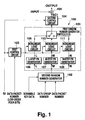
- Fig. 1 is a block diagram showing the overall constitution of a data processor 100 in an embodiment of the present invention.
- Fig. 2 shows a concrete circuit example of a first control circuit 103 and a nonlinear logic circuit 109 in the embodiment.
- Fig. 3 shows a constitutional example of a data packet.
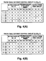
- Figs. 4(A) and 4(B) show truth tables for describing an operation of the first control circuit 103 in the embodiment.
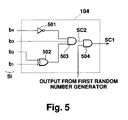
- Fig. 5 shows a concrete constitutional example of a second control circuit 104 in the embodiment.
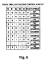
- Fig. 6 shows a truth table for describing the operation of the second control circuit 104 in the embodiment.
- Fig. 7 is a block diagram of an FM multiplex broadcasting receiver using the data processor in the embodiment.
- Fig. 8 shows another constitutional example of the first control circuit in the embodiment.
- Fig. 9 shows a state transition of the first control circuit shown in Fig. 8.
- Fig. 1 is a block diagram showing a schematic constitution of a data processor 100 in the embodiment.
- a first random number generator 101 outputs random numbers for scrambling or descrambling under the control of a first control circuit 103.
- a second random number generator 102 determines an initial value in accordance with scramble key data included in an FM multiplex broadcasting data, and it generates the random number, that is, a data to be input to the first random number generator 101, in accordance with a data group number and a data packet number included in a prefix.
- the first control circuit 103 executes an exclusive OR operation of a service identification code (SI) and low-order 4 bits of the data packet number, and supplies its output to nonlinear logic circuits (109 to 111).
- a second control circuit 104 controls whether the output from the first random number generator 101 is valid or invalid (zero output) in accordance with the service identification code (SI).
- SI service identification code
- a gate circuit 105 executes the exclusive OR operation of the FM multiplex broadcasting data and the output from the second control circuit 104.
- PN generators 106, 107, 108 generate an L-bit PN signal, an M-bit PN signal and an N-bit PN signal in accordance with the output from the second control circuit 104, respectively.
- the nonlinear logic circuits 109, 110, 111 receive the outputs from the PN generators 106, 107, 108 and the output from the first control circuit 103 as input signals, and they output a logic operation as a result of the input signals.
- a switch circuit 112 is controlled by the nonlinear logic circuit 110, and it outputs the PN signal corrected and controlled by the nonlinear logic circuit 109 or 111.
- the SI, the data packet number, the data group number and the scramble key data are determined in accordance with the data to be transmitted or the received data, and they are input to the data processor.
- the second random number generator 102 generates predetermined random numbers in accordance with the scramble key data, the data group number and the data packet number.
- the random numbers generated by the second random number generator 102 are divided into three, and the divided random numbers are supplied to the PN generators 106, 107, 108.
- the PN generators 106, 107, 108 use one part of the supplied random numbers, and they generate the corresponding PN signal independently.
- the outputs from the PN generators 106, 107, 108 are input to the nonlinear logic circuits 109, 110, 111, respectively.
- the signal from the first control circuit 103 is input to the respective nonlinear logic circuits 109, 110, 111.
- Each of the nonlinear logic circuits 109, 110, 111 executes a predetermined logical sum of the two signals to be input, and each nonlinear logic circuit outputs a 1-bit signal.
- the first control circuit 103 generates the signal from (the low-order 4 bits of) the data packet number.
- the outputs from the nonlinear logic circuits 109, 110, 111 are different from one another in accordance with the generated signal.
- the output from the first control circuit 103 is different. Accordingly, the outputs from the nonlinear logic circuits 109, 110, 111 are different from one another.
- the outputs from the nonlinear logic circuits 109, 110, 111 are input to the switch circuit 112.
- the switch circuit 112 selects the output from either nonlinear logic circuit 109 or 110 in accordance with the value from the nonlinear logic circuit 110. Accordingly, the 1-bit width random numbers are sequentially output as the output from the first random numbers generator 101 from the switch circuit 112. The random numbers are changed in accordance with the SI value.
- the output from the first random number generator 101 is input to the second control circuit 104.
- the SI is provided for the second control circuit 104.
- the second control circuit 104 controls whether or not the random numbers from the first random number generator 101 are output in accordance with the SI value.
- the output from the second control circuit 104 is provided for the gate circuit 105, and it is processed together with the input data. That is to say, at a transmitter side, the input data is the transmitted data to be scrambled. At a receiver side, the input data is the received data to be descrambled. The random numbers from the second control circuit 104 are processed together with the input data, whereby scrambling or descrambling processing is carried out.
- the second control circuit 104 controls whether or not the random numbers from the first random number generator 101 are output in accordance with the SI value. In the case where the service is not to be scrambled, the second control circuit 104 inhibits the output of the random numbers in accordance with the SI value. Accordingly, the scrambling or descrambling processing is not carried out in the gate circuit 105, and the input data is output as it is.
- the second control circuit 104 provides the random number from the first random number generator 101 for the gate circuit 105. Accordingly, the scrambling or descrambling processing is carried out in the gate circuit 105.
- the first control circuit 103 changes the output signal in accordance with the SI value. Accordingly, the random numbers output from the first random number generator 101 are changed in accordance with the SI value. Thus, the random numbers to be used for the scrambling processing can be easily changed in accordance with the contents of the service.
- Fig. 2 shows a concrete circuit example of the first control circuit 103 and the nonlinear logic circuit 109. Note that the nonlinear logic circuits 110 and 111 may also be the same as the nonlinear logic circuit 109.
- the first control circuit 103 comprises four exclusive OR circuits 201, 202, 203, 204.
- the 4-bit service identification codes (b1, b2, b3, b4) and the low-order four bits (b23, b24, b25, b26) of the data packet number are input to each of the exclusive OR circuits 201, 202, 203, 204, respectively.
- Each of the exclusive OR circuits executes the exclusive OR, and it outputs C1, C2, C3, C4. Accordingly, the outputs C1, C2, C3, C4 are determined in accordance with the SI value and (the low-order four bits of) the data packet number value, respectively.
- the AND gates 205, 206, 207, 208 are disposed in the nonlinear logic circuit 109, and they execute a logical product of the signal in the nonlinear logic circuit 109 and the outputs C1, C2, C3, C4.
- the AND gate 205 executes an AND of the output C1 and the inverted signal, that is, the second-bit signal from the PN generator 106 inverted by an inverter 211.
- the AND gate 206 executes the AND of the output C2 and the f-bit and g-bit signals from the PN generator 106.
- the AND gate 207 executes the AND of the output C3 and the inverted signal, that is, the i-bit signal from the PN generator 106 inverted by an inverter 212.
- the AND gate 208 executes the AND of the output C4 and the j-bit and k-bit signals from the PN generator 106.
- the outputs from the AND gates 206, 207 are input to an OR gate 209.
- the output from the AND gate 208 and the first-bit signal from the PN generator 106 are input to an OR gate 210.
- the first-bit signal from the PN generator 106, the outputs from the AND gates 205, 206 and the outputs from the OR gates 209, 210 are input to an exclusive OR circuit 213.
- the exclusive OR of the five signals is executed in the exclusive OR circuit 213, and it is output from the nonlinear logic circuit 109. In such a logic operation, the output from the PN generator 106 is modified in accordance with the SI value.
- Fig. 3 shows a constitutional example of the data packet.
- a 176-bit data packet comprises a prefix portion having a head of 32 bits (b1 to b32) and a data block portion having a tail of 144 bits.
- B1 to b4 in the prefix portion indicate the service identification number (SI)
- b9 to b22 indicate the data group number
- b23 to b32 indicate the data packet number.
- the SI, the data group number and the data packet number are determined in accordance with the data to be transmitted, and they are used so that the scrambling random numbers corresponding to the data packet are generated.
- the SI, the data group number and the data packet number are extracted from the prefix of the received data, and they are used so that the scrambling random numbers corresponding to the data packet are generated. Note that the scramble key data is also described at such a portion as to not be scrambled.
- Figs. 4(A) and 4(B) are truth tables for describing the operation of the first control circuit 103 shown in Fig. 2.
- Figs. 4(A) and 4(B) show such a case where there are only four kinds of the low-order four bits of the data packet number.
- the different outputs can be naturally obtained from the nonlinear logic circuits.
- Fig. 5 shows a concrete circuit example of the second control circuit 104.
- the second control circuit 104 comprises an inverter 501, an exclusive OR circuit 502 and AND gates 503, 504.
- B1 and b2 in SI are input to the exclusive OR circuit 502, and the output is input to the AND gate 503.
- b3 is input to the AND gate 503 as it is.
- B4 is inverted by the inverter 501, and it is input to the AND gate 503.
- the AND gate 503 executes the AND of the input three signals, and it outputs an output signal SC2.
- the output SC2 from the AND gate 503 and the output from the first random number generator 101 are input to the AND gate 504, and the AND gate 504 executes the AND of both these outputs.
- Fig. 6 is a truth table for describing the operation of the second control circuit.
- Fig. 7 is a block diagram of an FM multiplex broadcast receiver using the data processor in the embodiment.
- Fig. 7 shows an application example of the descrambling processing at the receiver side.
- the scrambling processing at the transmitter side of a broadcasting station is also substantially the same as the above method. That is, in the case of transmission, the output from the data processor is modulated and transmitted. In the case of reception, the received data is processed together with the random numbers so as to be descrambled.
- the signal which is transmitted from a desired station and received by an antenna 701 is extracted as an intermediate frequency (IF) signal at a front end 702.
- the signal is amplified in an IF amplifier 703, and it is detected in an FM detector 704.
- a usual FM broadcasting signal is output from the FM detector 704.
- the detected signal is also supplied to a 76-kHz band pass filter (BPF) 705, and an FM multiplex data signal is extracted.
- BPF band pass filter
- the signal output from the band pass filter 705 is demodulated in an L-MSK demodulating portion 706.
- the demodulated signal is regenerated in a synchronous reproducing circuit 707, and an error of the generated signal is corrected in an error correcting circuit 708.
- the corrected signal is supplied to the data processor 100 as the packet data. As described above, the descrambling processing is carried out.
- the output from the data processor 100 is supplied to an application microcomputer 709, where a necessary processing is carried out.
- the received FM multiplex data is displayed in a display 710.
- the first control circuit 103 is constituted of the four exclusive OR circuits, but this constitution is not restrictive.
- the first control circuit 103 may be constituted of a combination of the AND gate, the OR gate and the like, or a combination of a flip-flop circuit and the OR gate.
- Fig. 8 shows another constitutional example (example 2) of the first control circuit 103.
- the signals C1, C2, C3, C4 controlled by the SI alone are output. That is to say, this circuit is a PN generating circuit ( ⁇ 4+ ⁇ +1) in which the SI value is defined as the initial value.
- the first control circuit 103 comprises a timing generating circuit 801, flip-flop circuits 802, 803, 804, 805 and an exclusive OR circuit 806.
- the timing generating circuit 801 supplies a preset clock P which sets an initial timing (a timing in synchronization with the first random number generator 101) for generating the data and a clock CK in synchronization with a data clock to each preset terminal and clock input terminal of each flip-flop circuit 802 to 805. Furthermore, b1 to b4 in the SI is supplied to each initial value input terminal of each flip-flop circuit 802 to 805. Moreover, C1 to C4 are output from the flip-flop circuits 802 to 805, respectively.
- the output from the flip-flop circuit 805 is input to a data input terminal of the flip-flop circuit 802.
- the output from the flip-flop circuit 802 is input to the exclusive OR circuit 806.
- the output from the flip-flop circuit 805 is also input to the exclusive OR circuit 806.
- the exclusive OR of both the signals is executed in the exclusive OR circuit 806, and the output from the exclusive OR circuit 806 is input to the flip-flop circuit 803.
- the output from the flip-flop circuit 803 is input to the flip-flop circuit 804.
- the output from the flip-flop circuit 804 is input to the flip-flop circuit 805.
- the output states (C1, C2, C3, C4) are changed whenever the clock CK is input.
- the outputs (C1, C2, C3, C4) are (0, 1, 0, 1).
- the outputs (C1, C2, C3, C4) are (1, 1, 1, 0).
- the output states return to those of the first clock.
- Fig. 9 shows a state transition table of the first control circuit 103 in such a constitution.
- the nonlinear logic circuits 109, 110, 111 are controlled by the same first control circuit 103, but these nonlinear logic circuits 109, 110, 111 may also be controlled without any problem by a different first control circuit 103.
Landscapes
- Engineering & Computer Science (AREA)
- Signal Processing (AREA)
- Theoretical Computer Science (AREA)
- Computer Networks & Wireless Communication (AREA)
- Computer Security & Cryptography (AREA)
- Circuits Of Receivers In General (AREA)
- Two-Way Televisions, Distribution Of Moving Picture Or The Like (AREA)
Applications Claiming Priority (2)
| Application Number | Priority Date | Filing Date | Title |
|---|---|---|---|
| JP118032/96 | 1996-05-13 | ||
| JP11803296A JP3561574B2 (ja) | 1996-05-13 | 1996-05-13 | Fm多重放送のデータ加工装置 |
Publications (2)
| Publication Number | Publication Date |
|---|---|
| EP0808041A2 true EP0808041A2 (de) | 1997-11-19 |
| EP0808041A3 EP0808041A3 (de) | 1999-04-21 |
Family
ID=14726371
Family Applications (1)
| Application Number | Title | Priority Date | Filing Date |
|---|---|---|---|
| EP97303248A Withdrawn EP0808041A3 (de) | 1996-05-13 | 1997-05-13 | Datenverarbeitungsschaltung für die Verschlüsselung oder Entschlüsselung von Zusatzdaten eines Rundfunkprogramms |
Country Status (4)
| Country | Link |
|---|---|
| US (1) | US6128390A (de) |
| EP (1) | EP0808041A3 (de) |
| JP (1) | JP3561574B2 (de) |
| KR (1) | KR100255569B1 (de) |
Families Citing this family (4)
| Publication number | Priority date | Publication date | Assignee | Title |
|---|---|---|---|---|
| US7139397B2 (en) * | 2001-07-20 | 2006-11-21 | Stmicroelectronics S.R.L. | Hybrid architecture for realizing a random numbers generator |
| US8520851B2 (en) * | 2004-04-30 | 2013-08-27 | Blackberry Limited | Wireless communication device with securely added randomness and related method |
| JP5110956B2 (ja) * | 2007-05-10 | 2012-12-26 | 三菱電機株式会社 | 暗号化装置及び復号装置 |
| DE112013004985T5 (de) * | 2012-10-12 | 2015-07-09 | National Instruments Ireland Resources Limited | System und Verfahren zum Kalibrieren und Synchronisieren eines Empfängers |
Family Cites Families (9)
| Publication number | Priority date | Publication date | Assignee | Title |
|---|---|---|---|---|
| US4811394A (en) * | 1982-07-28 | 1989-03-07 | Communications Satellite Corporation | Variable starting state scrambling circuit |
| JP2581440B2 (ja) * | 1994-05-11 | 1997-02-12 | 日本電気株式会社 | スクランブル通信方式 |
| US5740246A (en) * | 1994-12-13 | 1998-04-14 | Mitsubishi Corporation | Crypt key system |
| JP3294739B2 (ja) * | 1995-03-30 | 2002-06-24 | 三洋電機株式会社 | Fm多重放送のスクランブルまたはデスクランブル方法 |
| FR2735311B1 (fr) * | 1995-06-07 | 1997-08-14 | Telediffusion Fse | Protocole d'emission de messages de controle d'acces a des applications rds, dispositifs d'emission et de reception correspondants. |
| SE518747C2 (sv) * | 1995-08-28 | 2002-11-12 | Sanyo Electric Co | Digital signalmottagare som kan mottaga data som har kodats och sänts med on-line behandling |
| JP3625540B2 (ja) * | 1995-09-11 | 2005-03-02 | 三洋電機株式会社 | スクランブル解除装置 |
| JP3059918B2 (ja) * | 1995-09-11 | 2000-07-04 | 三洋電機株式会社 | Fm多重放送受信機におけるデータ加工装置 |
| US5835499A (en) * | 1995-09-11 | 1998-11-10 | Sanyo Electric Co., Ltd. | Data processing device for FM multi-channel broadcasting |
-
1996
- 1996-05-13 JP JP11803296A patent/JP3561574B2/ja not_active Expired - Fee Related
-
1997
- 1997-05-12 US US08/854,602 patent/US6128390A/en not_active Expired - Lifetime
- 1997-05-12 KR KR1019970018311A patent/KR100255569B1/ko not_active Expired - Fee Related
- 1997-05-13 EP EP97303248A patent/EP0808041A3/de not_active Withdrawn
Also Published As
| Publication number | Publication date |
|---|---|
| US6128390A (en) | 2000-10-03 |
| KR100255569B1 (ko) | 2000-05-01 |
| JPH09307514A (ja) | 1997-11-28 |
| EP0808041A3 (de) | 1999-04-21 |
| KR970078061A (ko) | 1997-12-12 |
| JP3561574B2 (ja) | 2004-09-02 |
Similar Documents
| Publication | Publication Date | Title |
|---|---|---|
| EP0372499B1 (de) | Vorrichtung und Verfahren für Digitalton in dem FM-Rundfunkband | |
| US4531021A (en) | Two level encripting of RF signals | |
| KR100398718B1 (ko) | Fm다중방송의스크램블또는디스크램블방법 | |
| US4864614A (en) | Authorising coded signals | |
| CA2121565C (en) | Data broadcasting system | |
| US5333155A (en) | Method and system for transmitting digital audio signals from recording studios to the various master stations of a broadcasting network | |
| CN1274495A (zh) | 用于在音频无线电广播系统中减轻断续中断的系统和方法 | |
| US5544198A (en) | Procedure for the identification of transmitter or region in common-wave broadcasting networks | |
| EP0735787A2 (de) | Rufempfänger für FM-Multiplexrundfunk | |
| US4991207A (en) | One-way address transmission system of PCM music | |
| JPH10508162A (ja) | 多重サブキャリアを使用するデジタルデータ送信 | |
| US6128390A (en) | Data processor for FM multiplex broadcast | |
| US4688247A (en) | Pay TV scrambling by audio encryption | |
| NO323054B1 (no) | Digital signalmottaker som kan motta data som er krypterte og sendt i direkte behandling | |
| US7123875B1 (en) | System and method for multipoint distribution of satellite digital audio radio service | |
| ES8702756A1 (es) | Procedimiento de difusion de datos,tales como informaciones escritas de los datos numericos o alfanumericos o logiciales y sistema para poner en practica dicho procedimiento | |
| US5740518A (en) | FM character data multiplex broadcasting signal receiving apparatus | |
| MY137369A (en) | Receiver unit and method of setting the same | |
| KR100235428B1 (ko) | Fm 다중 방송에서의 데이타 가공 장치 | |
| US5960328A (en) | FM radio receiver and signal processing device used therein | |
| KR0173551B1 (ko) | Fm 수신기 및 이것에 이용되는 신호 처리 장치 | |
| JPH0511810B2 (de) | ||
| CN1134645A (zh) | 有线电视的加密方法 | |
| JP2885809B2 (ja) | 受信機 | |
| JP3373984B2 (ja) | デジタル信号受信装置 |
Legal Events
| Date | Code | Title | Description |
|---|---|---|---|
| PUAI | Public reference made under article 153(3) epc to a published international application that has entered the european phase |
Free format text: ORIGINAL CODE: 0009012 |
|
| AK | Designated contracting states |
Kind code of ref document: A2 Designated state(s): AT CH DE FR LI NL SE |
|
| PUAL | Search report despatched |
Free format text: ORIGINAL CODE: 0009013 |
|
| AK | Designated contracting states |
Kind code of ref document: A3 Designated state(s): AT CH DE FR LI NL SE |
|
| STAA | Information on the status of an ep patent application or granted ep patent |
Free format text: STATUS: THE APPLICATION IS DEEMED TO BE WITHDRAWN |
|
| 18D | Application deemed to be withdrawn |
Effective date: 19991022 |