EP0807983A2 - Dispositif semi-conducteur ayant une couche semi-conducteur du type II-VI contenant du tellure - Google Patents
Dispositif semi-conducteur ayant une couche semi-conducteur du type II-VI contenant du tellure Download PDFInfo
- Publication number
- EP0807983A2 EP0807983A2 EP97107468A EP97107468A EP0807983A2 EP 0807983 A2 EP0807983 A2 EP 0807983A2 EP 97107468 A EP97107468 A EP 97107468A EP 97107468 A EP97107468 A EP 97107468A EP 0807983 A2 EP0807983 A2 EP 0807983A2
- Authority
- EP
- European Patent Office
- Prior art keywords
- layer
- inp substrate
- semiconductor device
- znsete
- buffer layer
- Prior art date
- Legal status (The legal status is an assumption and is not a legal conclusion. Google has not performed a legal analysis and makes no representation as to the accuracy of the status listed.)
- Withdrawn
Links
Images

Classifications
-
- H—ELECTRICITY
- H10—SEMICONDUCTOR DEVICES; ELECTRIC SOLID-STATE DEVICES NOT OTHERWISE PROVIDED FOR
- H10H—INORGANIC LIGHT-EMITTING SEMICONDUCTOR DEVICES HAVING POTENTIAL BARRIERS
- H10H20/00—Individual inorganic light-emitting semiconductor devices having potential barriers, e.g. light-emitting diodes [LED]
- H10H20/01—Manufacture or treatment
- H10H20/011—Manufacture or treatment of bodies, e.g. forming semiconductor layers
- H10H20/012—Manufacture or treatment of bodies, e.g. forming semiconductor layers having light-emitting regions comprising only Group II-IV materials
- H10H20/0125—Manufacture or treatment of bodies, e.g. forming semiconductor layers having light-emitting regions comprising only Group II-IV materials with a substrate not being Group II-VI materials
Definitions
- the present invention relates to a semiconductor device which includes an InP substrate and a II-VI compound semiconductor layer containing Te, and more particularly to a semiconductor device which can be used as a light emitting device and which has a II-VI compound semiconductor layer containing Te.
- III-V compound semiconductors containing Group III elements such as Al, Ga, In, etc. and Group V elements such as As, P, Sb, etc. in a periodic table
- semiconductor lasers for emitting laser beams of wavelengths in the ranges from infrared rays up to red light, light emitting diodes for emitting light of wavelengths in the ranges up to yellow-green light, and/or the like have been brought into practical use.
- a larger bandgap energy band is required.
- the above-described III-V compound semiconductors cannot satisfy this requirement.
- II-VI compound semicondutors containing Group II elements such as Zn, Cd, Mg, etc. and Group VI elements such as S, Se, Te, etc. have relatively large bandgap energy, and can emit light of almost all wavelengths in a visible region.
- the II-VI compound semiconductors are anticipated as the materials of light emitting devices for emitting light of wavelengths in the ranges especially from green light up to ultraviolet rays, and in recent years, researches and development have been actively performed.
- a high-quality III-V bulk substrate crystal the access to which is easy, is generally used as a substrate.
- a GaAs substrate has a lattice constant approximate to that of ZnSe which is one of the II-VI compound semiconductors. Using mixed crystals like ZnSSe and MgZnSSe, therefore, a double heterostructure can be formed under the lattice-matching condition.
- the GaAs substrate is most widely used as the substrate for a II-VI compound semiconductor growth.
- the lattices of ZnSeTe or MgZnSeTe among the II-VI mixed crystals containing Te do not match with those of the GaAs substrate most commonly used in the prior art, under which condition it is difficult to form a high-quality crystal.
- a lattice-matched mixed crystal can be grown if an InP substrate is employed.
- ZnSeTe or MgZnSeTe when being grown on the InP substrate so that the lattice thereof aligns with that of the InP substrate, has orange to ultraviolet band gap wavelengths (2.1 eV to 3.5 eV), and therefore is also anticipated as the material of a short-wavelength laser diode (LD). If a laser diode structure including a p-type cladding layer of such a mixed crystal can be formed on an InP substrate, the insufficiency of a p-type carrier concentration, which is a drawback of a II-VI light emitting device on the convensional GaAs substrate, can be solved.
- LD short-wavelength laser diode
- Fig. 1 shows a semiconductor device wherein a ZnSeTe layer 3 is formed on an InP substrate by convensional method MBE (molecular beam epitaxy).
- MBE molecular beam epitaxy
- the ZnSeTe layer 3 grows three-dimensionally for one minute or more directly after the start of growing, and then grows two-dimensionally.
- the three dimensionally growth mode causes a large number of crystal defects, and is not desirable in the application of devices.
- the full width at half maximum of the double crystal X-ray diffraction rocking curve (XRC) of the layer as formed is 150 sec or wider, the emission intensity of photoluminescence (PL) is very weak, and the quality of crystal is problematic in use as a light emitting device.
- a semiconductor device comprises an InP substrate, a ZnCdSe buffer layer formed on the InP substrate, and a II-VI compound semiconductor layer containing Te and formed on the ZnCdSe buffer layer.
- a native oxide layer on a surface of the InP substrate is removed, a ZnCdSe buffer layer is deposited, and then a II-VI thin film containing Te is grown on the ZnCdSe buffer layer.
- the ZnCdSe layer which is easier than ZnSeTe in two-dimensionally growth from directly after the start of growing is grown as a buffer layer. This ensures considerably improved quality of the II-VI mixed crystal containing Te and which is grown on the ZnCdSe buffer layer.
- the substrate temperature is raised, with the Se irradiation being performed, up to the temperature at which the II-VI layer containing Te is grown. After the substrate temperature has became stable, the growing of the layer is initiated. Under these conditions, a high-quality II-VI layer is easily obtained.
- Use of a substrate formed by depositing a GaInAs buffer layer on InP substrate facilitates the removal of the native oxide layer on the surface of the substrate, and therefore is more advantageous.
- the above-described advantages do not depend on the thickness of the ZnCdSe layer.
- the thickness of the ZnCdSe layer be less than such a critical thickness that crystal defects due to lattice-mismatching to InP substrate would occur.
- Fig. 2 shows the semiconductor device according to the first embodiment of the present invention.
- This semiconductor device includes an InP substrate 1, a ZnCdSe buffer layer 2 grown on the InP substrate, and a ZnSeTe layer 3 grown on the ZnCdSe buffer layer 2 as a II-VI compound semiconductor layer containing Te.
- the above semiconductor device is manufactured in the following manner. After the removal of the native oxide layer on a surface of the InP substrate 1, the ZnCdSe buffer layer 2 having a given composition is grown, and the ZnSeTe layer 3 lattice-matched with the InP substrate 1 is formed on the ZnCdSe buffer layer 2.
- the ZnSeTe layer 3 when a growing surface thereof is observed by RHEED, grows two-dimensionally directly after the start of growing, and high quality ZnSeTe layer 3 having few crystal defects is obtained.
- the thickness (film thickness) of the ZnCdSe buffer layer 2 is set less than a critical thickness (critical film thickness) so that crystal defects due to lattice-mismatching between the InP substrate 1 and the ZnCdSe buffer layer 2 do not occur.
- a critical thickness critical film thickness
- the film thickness of the ZnCdSe buffer layer 2 is on the order of 0.1 ⁇ m which is less than a critical film thickness of, in this case, 0.15 ⁇ m.
- the critical film thickness of the ZnCdSe buffer layer 2 varies in accordance with the degree of lattice-mismatching between the InP substrate 1 and the ZnCdSe buffer layer 2, and can be calculated by, for example, the dynamical equilibrium theory studied by Matthews and Blakeslee and described in the Journal of Crystal Growth, Vol. 27, p.118, 1974.
- the ZnSeTe layer 3 whose lattice constant is matched with that of the InP substrate 1, is formed on the ZnCdSe buffer layer 2, it can be confirmed by the surface observation by RHEED that the ZnSeTe layer 3 grows two-dimensionally from directly after the start of growing, and high quality ZnSeTe layer 3 having few crystal defects is attained.
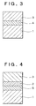
- Fig. 3 is a sectional view of the semiconductor device according to the second embodiment of the present invention.
- This semiconductor device includes an InP substrate 1, an Zn 0.48 Cd 0.52 Se buffer layer 4 grown on the InP substrate 1, and a ZnSeTe layer 3 grown on the Zn 0.48 Cd 0.52 Se buffer layer 4 as a II-VI compound semiconductor layer containing Te.
- This semiconductor device is manufactured in the following manner. After the removal of the native oxide layer on a surface of the InP substrate 1, the Zn 0.48 Cd 0.52 Se buffer layer 4 having such a composition that the lattice constant thereof substantially match with that of the InP substrate 1, is deposited on the InP substrate 1, and the ZnSeTe layer 3 lattice-matched with the InP substrate 1 is grown on the Zn 0.48 Cd 0.52 Se buffer layer 4.
- the ZnSeTe layer 3 when a growing surface thereof is observed by RHEED, grows two-dimensionally from directly after the start of growing, and high quality ZnSeTe layer 3 having few crystal defects is attained.
- the full width at half maximum of the double crystal X-ray diffraction rocking curve of the ZnSeTe layer 3 is on the order of 50 sec., which is not greater than 1/3 that of the prior art.
- the emission intensity of photoluminescence is at least one thousand times that of the ZnSeTe layer grown by the convensional method on the InP substrate.
- the ZnSeTe layer of considerably high quality which is applicable to a light emitting device, is obtained.
- the present invention is applicable also to the case where in place of the ZnSeTe layer 3, another II-VI compound semiconductor layer like MgZnSeTe, MgZnSTe, MgCdSTe, ZnCdSeTe, ZnCdSTe, etc., whose lattice constant are matched with that of the InP substrate 1, is formed above the InP substrate 1.
- the present invention is advantageous irrespective of the conductivity type of the ZnCdSe buffer layer 2 and the kind of an added impurity in the ZnCdSe buffer layer 2.
- a substrate formed by depositing a III-V compound semiconductor buffer layer like InGaAs on the InP substrate 1 may be used as a substrate on/above which the ZnCdSe buffer layer 2 is deposited.
- Fig. 4 shows a semiconductor device wherein an InGaAs layer 5 is formed on the InP substrate as the III-V compound semiconductor buffer layer and wherein a ZnCdSe buffer layer 2 and a ZnSeTe layer 3 are formed on/above the InGaAs layer 5.
- This semiconductor device has the same advantages as those of the semiconductor devices shown in Figs. 2 and 3.
Landscapes
- Led Devices (AREA)
- Semiconductor Lasers (AREA)
Applications Claiming Priority (3)
| Application Number | Priority Date | Filing Date | Title |
|---|---|---|---|
| JP11683696 | 1996-05-10 | ||
| JP11683696A JP2803722B2 (ja) | 1996-05-10 | 1996-05-10 | 半導体装置及びその製造方法 |
| JP116836/96 | 1996-05-10 |
Publications (2)
| Publication Number | Publication Date |
|---|---|
| EP0807983A2 true EP0807983A2 (fr) | 1997-11-19 |
| EP0807983A3 EP0807983A3 (fr) | 2000-04-26 |
Family
ID=14696834
Family Applications (1)
| Application Number | Title | Priority Date | Filing Date |
|---|---|---|---|
| EP97107468A Withdrawn EP0807983A3 (fr) | 1996-05-10 | 1997-05-06 | Dispositif semi-conducteur ayant une couche semi-conducteur du type II-VI contenant du tellure |
Country Status (3)
| Country | Link |
|---|---|
| US (1) | US5773850A (fr) |
| EP (1) | EP0807983A3 (fr) |
| JP (1) | JP2803722B2 (fr) |
Cited By (1)
| Publication number | Priority date | Publication date | Assignee | Title |
|---|---|---|---|---|
| EP1760850A3 (fr) * | 2005-09-05 | 2009-05-06 | Sophia School Corporation | Structure semiconductrice optique sur un substrat d'InP |
Families Citing this family (6)
| Publication number | Priority date | Publication date | Assignee | Title |
|---|---|---|---|---|
| US6178190B1 (en) * | 1997-08-04 | 2001-01-23 | Nec Corporation | II-VI compound semiconductor light emitting device |
| US6049099A (en) * | 1998-05-11 | 2000-04-11 | The United States Of America As Represented By The Secretary Of The Air Force | Cadmium sulfide layers for indium phosphide-based heterojunction bipolar transistors |
| JP3399392B2 (ja) * | 1999-02-19 | 2003-04-21 | 株式会社村田製作所 | 半導体発光素子、およびその製造方法 |
| US20110155208A1 (en) * | 2008-06-25 | 2011-06-30 | Michael Wang | Semiconductor heterojunction photovoltaic solar cell with a charge blocking layer |
| US8664524B2 (en) | 2008-07-17 | 2014-03-04 | Uriel Solar, Inc. | High power efficiency, large substrate, polycrystalline CdTe thin film semiconductor photovoltaic cell structures grown by molecular beam epitaxy at high deposition rate for use in solar electricity generation |
| US10077991B2 (en) | 2016-09-27 | 2018-09-18 | Mitutoyo Corporation | Optical encoder configured to mitigate undesired interfering light components |
Family Cites Families (5)
| Publication number | Priority date | Publication date | Assignee | Title |
|---|---|---|---|---|
| JPH02125477A (ja) * | 1988-11-04 | 1990-05-14 | Oki Electric Ind Co Ltd | 可視光発光素子 |
| US5081632A (en) * | 1989-01-26 | 1992-01-14 | Hitachi, Ltd. | Semiconductor emitting device |
| AU4104293A (en) * | 1992-05-19 | 1993-12-13 | California Institute Of Technology | Wide band-gap semiconductor light emitters |
| US5488233A (en) * | 1993-03-11 | 1996-01-30 | Kabushiki Kaisha Toshiba | Semiconductor light-emitting device with compound semiconductor layer |
| JPH07254755A (ja) * | 1994-03-16 | 1995-10-03 | Hitachi Ltd | 半導体発光素子 |
-
1996
- 1996-05-10 JP JP11683696A patent/JP2803722B2/ja not_active Expired - Fee Related
-
1997
- 1997-05-06 EP EP97107468A patent/EP0807983A3/fr not_active Withdrawn
- 1997-05-07 US US08/852,283 patent/US5773850A/en not_active Expired - Fee Related
Cited By (2)
| Publication number | Priority date | Publication date | Assignee | Title |
|---|---|---|---|---|
| EP1760850A3 (fr) * | 2005-09-05 | 2009-05-06 | Sophia School Corporation | Structure semiconductrice optique sur un substrat d'InP |
| US7772586B2 (en) | 2005-09-05 | 2010-08-10 | Sophia School Corporation | Optical semiconductor devices on InP substrate |
Also Published As
| Publication number | Publication date |
|---|---|
| EP0807983A3 (fr) | 2000-04-26 |
| JPH09307142A (ja) | 1997-11-28 |
| JP2803722B2 (ja) | 1998-09-24 |
| US5773850A (en) | 1998-06-30 |
Similar Documents
| Publication | Publication Date | Title |
|---|---|---|
| US8507365B2 (en) | Growth of coincident site lattice matched semiconductor layers and devices on crystalline substrates | |
| Ponce et al. | Homoepitaxy of GaN on polished bulk single crystals by metalorganic chemical vapor deposition | |
| Matsuoka et al. | Wide-gap semiconductor InGaN and InGaAln grown by MOVPE | |
| US6072189A (en) | III-nitride optoelectronic semiconductor device containing Lattice mismatched III-nitride semiconductor materials | |
| DE69738008T2 (de) | Halbleiterbauelement | |
| EP0977279A2 (fr) | AlGaInN LED et laser à diode | |
| Gokhale et al. | Growth and characterization of small band gap (∼ 0.6 eV) InGaAsN layers on InP | |
| Luo et al. | Molecular beam epitaxy of a low strain II‐VI heterostructure: ZnTe/CdSe | |
| EP0487822B1 (fr) | Elément semi-conducteur émettant de la lumière | |
| Fujita et al. | Lattice-mismatch effects on properties in ZnSe layer grown on GaAs substrate by low pressure OMVPE | |
| US5773850A (en) | Semiconductor device having a ZnCdSe buffer layer with a II-VI compound semiconductor layer containing Te grown thereon | |
| Razeghi et al. | Disorder of a GaxIn1-xAsyP1-y-InP quantum well by Zn diffusion | |
| Zyskind et al. | Liquid‐phase‐epitaxial InAs y Sb1− y on GaSb substrates using GaInAsSb buffer layers: Growth, characterization, and application to mid‐IR photodiodes | |
| Maksimov et al. | Be‐Chalcogenide Alloys for Improved R‐G‐B LEDs: BexZnyCd1–x–ySe on InP | |
| EP0487823A2 (fr) | Dispositif émetteur de lumière à semi-conducteur | |
| US6072202A (en) | II-VI compound semiconductor device with III-V buffer layer | |
| JP3334598B2 (ja) | InP基板上II−VI族化合物半導体薄膜 | |
| JP3333346B2 (ja) | 半導体装置 | |
| Xiuying et al. | Liquid phase epitaxy growth and properties of GaInAsSb/AlGaAsSb/GaSb heterostructures | |
| JP2001015803A (ja) | AlGaInP発光ダイオード | |
| US5540786A (en) | Light emitting material | |
| JP2653901B2 (ja) | 化合物半導体発光素子 | |
| Tomasulo et al. | Molecular beam epitaxy of wide-bandgap InAlAsSb on InP substrates for an all lattice-matched triple-junction solar cell | |
| Haque et al. | Study of Nonradiative Recombination Centers in n-GaN Grown on LT-GaN and AlN Buffer Layer by Below-Gap Excitation | |
| JP2644992B2 (ja) | 化合物半導体結晶の製造方法 |
Legal Events
| Date | Code | Title | Description |
|---|---|---|---|
| PUAI | Public reference made under article 153(3) epc to a published international application that has entered the european phase |
Free format text: ORIGINAL CODE: 0009012 |
|
| AK | Designated contracting states |
Kind code of ref document: A2 Designated state(s): DE GB |
|
| PUAL | Search report despatched |
Free format text: ORIGINAL CODE: 0009013 |
|
| AK | Designated contracting states |
Kind code of ref document: A3 Designated state(s): DE GB |
|
| RIC1 | Information provided on ipc code assigned before grant |
Free format text: 7H 01L 33/00 A, 7H 01S 3/19 B |
|
| 17P | Request for examination filed |
Effective date: 20000317 |
|
| 17Q | First examination report despatched |
Effective date: 20031113 |
|
| STAA | Information on the status of an ep patent application or granted ep patent |
Free format text: STATUS: THE APPLICATION HAS BEEN WITHDRAWN |
|
| 18W | Application withdrawn |
Effective date: 20031222 |