EP0807295B1 - Connector for a smart card reader apparatus and card reader comprising same - Google Patents
Connector for a smart card reader apparatus and card reader comprising same Download PDFInfo
- Publication number
- EP0807295B1 EP0807295B1 EP96902309A EP96902309A EP0807295B1 EP 0807295 B1 EP0807295 B1 EP 0807295B1 EP 96902309 A EP96902309 A EP 96902309A EP 96902309 A EP96902309 A EP 96902309A EP 0807295 B1 EP0807295 B1 EP 0807295B1
- Authority
- EP
- European Patent Office
- Prior art keywords
- contact elements
- card
- connector
- electronic circuit
- microcircuit
- Prior art date
- Legal status (The legal status is an assumption and is not a legal conclusion. Google has not performed a legal analysis and makes no representation as to the accuracy of the status listed.)
- Expired - Lifetime
Links
- 238000003780 insertion Methods 0.000 claims abstract description 9
- 230000037431 insertion Effects 0.000 claims abstract description 9
- 238000001514 detection method Methods 0.000 claims description 7
- 239000012777 electrically insulating material Substances 0.000 claims description 2
- 230000000903 blocking effect Effects 0.000 claims 1
- 230000006870 function Effects 0.000 description 14
- 238000012360 testing method Methods 0.000 description 6
- 238000000034 method Methods 0.000 description 3
- 230000005540 biological transmission Effects 0.000 description 2
- 238000011161 development Methods 0.000 description 2
- 238000005538 encapsulation Methods 0.000 description 2
- 235000021183 entrée Nutrition 0.000 description 2
- 230000010354 integration Effects 0.000 description 2
- 238000007726 management method Methods 0.000 description 2
- 238000003466 welding Methods 0.000 description 2
- 208000031968 Cadaver Diseases 0.000 description 1
- 240000008042 Zea mays Species 0.000 description 1
- 238000012550 audit Methods 0.000 description 1
- 238000010276 construction Methods 0.000 description 1
- 238000007796 conventional method Methods 0.000 description 1
- 230000007547 defect Effects 0.000 description 1
- 238000013461 design Methods 0.000 description 1
- 230000006866 deterioration Effects 0.000 description 1
- 238000006073 displacement reaction Methods 0.000 description 1
- 230000000694 effects Effects 0.000 description 1
- 239000012634 fragment Substances 0.000 description 1
- 238000010348 incorporation Methods 0.000 description 1
- 238000009413 insulation Methods 0.000 description 1
- 239000000463 material Substances 0.000 description 1
- 238000005259 measurement Methods 0.000 description 1
- 238000012986 modification Methods 0.000 description 1
- 230000004048 modification Effects 0.000 description 1
- 210000000056 organ Anatomy 0.000 description 1
- 238000012545 processing Methods 0.000 description 1
- 230000004044 response Effects 0.000 description 1
- 239000004065 semiconductor Substances 0.000 description 1
- 238000012163 sequencing technique Methods 0.000 description 1
- 238000012795 verification Methods 0.000 description 1
Images


Classifications
-
- G—PHYSICS
- G06—COMPUTING; CALCULATING OR COUNTING
- G06K—GRAPHICAL DATA READING; PRESENTATION OF DATA; RECORD CARRIERS; HANDLING RECORD CARRIERS
- G06K7/00—Methods or arrangements for sensing record carriers, e.g. for reading patterns
- G06K7/06—Methods or arrangements for sensing record carriers, e.g. for reading patterns by means which conduct current when a mark is sensed or absent, e.g. contact brush for a conductive mark
-
- H—ELECTRICITY
- H01—ELECTRIC ELEMENTS
- H01R—ELECTRICALLY-CONDUCTIVE CONNECTIONS; STRUCTURAL ASSOCIATIONS OF A PLURALITY OF MUTUALLY-INSULATED ELECTRICAL CONNECTING ELEMENTS; COUPLING DEVICES; CURRENT COLLECTORS
- H01R13/00—Details of coupling devices of the kinds covered by groups H01R12/70 or H01R24/00 - H01R33/00
- H01R13/02—Contact members
- H01R13/22—Contacts for co-operating by abutting
- H01R13/24—Contacts for co-operating by abutting resilient; resiliently-mounted
- H01R13/2442—Contacts for co-operating by abutting resilient; resiliently-mounted with a single cantilevered beam
-
- E—FIXED CONSTRUCTIONS
- E04—BUILDING
- E04B—GENERAL BUILDING CONSTRUCTIONS; WALLS, e.g. PARTITIONS; ROOFS; FLOORS; CEILINGS; INSULATION OR OTHER PROTECTION OF BUILDINGS
- E04B2/00—Walls, e.g. partitions, for buildings; Wall construction with regard to insulation; Connections specially adapted to walls
- E04B2/74—Removable non-load-bearing partitions; Partitions with a free upper edge
- E04B2/7407—Removable non-load-bearing partitions; Partitions with a free upper edge assembled using frames with infill panels or coverings only; made-up of panels and a support structure incorporating posts
- E04B2/7453—Removable non-load-bearing partitions; Partitions with a free upper edge assembled using frames with infill panels or coverings only; made-up of panels and a support structure incorporating posts with panels and support posts, extending from floor to ceiling
-
- G—PHYSICS
- G06—COMPUTING; CALCULATING OR COUNTING
- G06K—GRAPHICAL DATA READING; PRESENTATION OF DATA; RECORD CARRIERS; HANDLING RECORD CARRIERS
- G06K7/00—Methods or arrangements for sensing record carriers, e.g. for reading patterns
- G06K7/0013—Methods or arrangements for sensing record carriers, e.g. for reading patterns by galvanic contacts, e.g. card connectors for ISO-7816 compliant smart cards or memory cards, e.g. SD card readers
- G06K7/0021—Methods or arrangements for sensing record carriers, e.g. for reading patterns by galvanic contacts, e.g. card connectors for ISO-7816 compliant smart cards or memory cards, e.g. SD card readers for reading/sensing record carriers having surface contacts
-
- G—PHYSICS
- G06—COMPUTING; CALCULATING OR COUNTING
- G06K—GRAPHICAL DATA READING; PRESENTATION OF DATA; RECORD CARRIERS; HANDLING RECORD CARRIERS
- G06K7/00—Methods or arrangements for sensing record carriers, e.g. for reading patterns
- G06K7/0013—Methods or arrangements for sensing record carriers, e.g. for reading patterns by galvanic contacts, e.g. card connectors for ISO-7816 compliant smart cards or memory cards, e.g. SD card readers
- G06K7/0056—Methods or arrangements for sensing record carriers, e.g. for reading patterns by galvanic contacts, e.g. card connectors for ISO-7816 compliant smart cards or memory cards, e.g. SD card readers housing of the card connector
- G06K7/0069—Methods or arrangements for sensing record carriers, e.g. for reading patterns by galvanic contacts, e.g. card connectors for ISO-7816 compliant smart cards or memory cards, e.g. SD card readers housing of the card connector including means for detecting correct insertion of the card, e.g. end detection switches notifying that the card has been inserted completely and correctly
-
- H—ELECTRICITY
- H01—ELECTRIC ELEMENTS
- H01R—ELECTRICALLY-CONDUCTIVE CONNECTIONS; STRUCTURAL ASSOCIATIONS OF A PLURALITY OF MUTUALLY-INSULATED ELECTRICAL CONNECTING ELEMENTS; COUPLING DEVICES; CURRENT COLLECTORS
- H01R13/00—Details of coupling devices of the kinds covered by groups H01R12/70 or H01R24/00 - H01R33/00
- H01R13/66—Structural association with built-in electrical component
- H01R13/665—Structural association with built-in electrical component with built-in electronic circuit
-
- E—FIXED CONSTRUCTIONS
- E04—BUILDING
- E04B—GENERAL BUILDING CONSTRUCTIONS; WALLS, e.g. PARTITIONS; ROOFS; FLOORS; CEILINGS; INSULATION OR OTHER PROTECTION OF BUILDINGS
- E04B2/00—Walls, e.g. partitions, for buildings; Wall construction with regard to insulation; Connections specially adapted to walls
- E04B2/74—Removable non-load-bearing partitions; Partitions with a free upper edge
- E04B2002/7481—Locating rails with adjustable curvature
Definitions
- the invention relates to a connector for a card reader device. microcircuit.
- the invention also relates to a card reader device with microcircuit comprising such a connector.
- the term “card” means all the cards comprising a monolithic or hybrid integrated circuit, called “chip”. This is, by example, a card in the “credit card” format, also known under the name “CAM” (Memory Card “).
- the microcircuit on the card includes a microprocessor or a microcontroller, comprising, in particular circuits for memory, for example of the "PROM” type.
- This type of card is intended to be inserted in specific data reading and / or writing devices. To simplify, these devices will be called “readers” in the following, it being understood that can also write data and other related functions (power supply, tests, etc.)
- the data is stored in the aforementioned memory circuits, generally in encrypted form. They are therefore read at from memory positions or on the contrary written in these memory positions.
- input-output members constituted by contact pads flush with the surface of one of the main faces of the card.
- Various standards define the position of these contact pads. They serve, no only for the above-mentioned data inputs and outputs, but also for the supply of electrical energy to the microcircuit as well as for carrying out various verifications, depending on the applications considered (presence test, etc.).
- the reader includes brush contacts which come into galvanic contact with the pads above, when the card is correctly inserted in a connector provided for this effect.
- the first category consists of detection systems electronic.
- an electrical test is carried out, for example the resistance measurement between the brush contacts. If these tests do not match expected values, in a given range, it is deduced from this that the card is inserted incorrectly or that an object stranger is introduced in his place.
- the second category consists of so-called "to landing".
- An example of such a system is described in the patent application French FR-A-2 628 901.
- the card is positioned against a stop before contacting the brushes. Contact is made by relative displacement from the card to the brushes, perpendicular to the surface of the card (faces main).
- the third category consists of brush contact systems rubbing with "limit switch" contact. Such a system is disclosed, for example, by French patent application FR-A-2 623 314.
- the connectors in which are cards inserted have a "limit switch” contact which triggers the bet on the microcircuit when the card is in the correct position.
- the mechanical arrangement is simple and inexpensive, however it has at least the disadvantage of requiring the incorporation, in the electronics of the reader, circuits for managing the aforementioned "limit switch" contact.
- the invention sets itself the goal of providing a solution to the problems mentioned above, while overcoming the disadvantages of Art systems Known.
- the connector for a card reader device microcircuit comprising a body supporting brush contact elements intended to be brought into electrical contact with conductive pads associated with said microcircuit of the card when it is inserted in the connector; at least one part of the brush contact elements being connected to an electronic circuit comprising means for controlling operations of insertion or removal of the card in the reader, said circuit being connected, on the other hand, with the electronic circuit the card reader; said connector being characterized in that it comprises and carries said electronic circuit.
- the invention also relates to a card reader device comprising such a connector.
- the connector according to the invention carries itself and not the reader, an electronic circuit which makes it possible to control the various operations inserting or removing the card in the card reader.
- the connector 1 for a card reader device C with a microcircuit 3 comprises a body 2 supporting brush contact elements C 1 to C 8 , intended to be brought into electrical contact with conductive pads associated with said microcircuit I C when card C is inserted in connector 1.
- this connector 1 comprises an electronic circuit I C connected, on the one hand, with at least part of said brush contact elements C 1 to C 8 and, on the other hand, with the electronic circuit 4 of the card reader.
- the electronic circuit I C carried by the connector 1 comprises means which will be detailed below to control operations of insertion or removal of the card C in the card reader.
- Figure 2 schematically illustrates, in exploded view, the arrangement of a connector 1 according to a particular embodiment of the invention. More specifically, in this figure, only the provisions relating to the different connector contact elements.
- the circuit I C there is an integrated circuit I C within the same connector 1. More specifically, the circuit I C is arranged in a housing formed in the thickness of the insulation of the connector frame (not shown in this figure).
- the connector includes two sets of contact elements.
- a first set located substantially in a first plane P 1 , or lower plane in FIG. 2, comprises a series of pairs of brush contacts; four pairs in the example illustrated, C 1 to C 8 .
- These brush contacts, C 1 to C 8 consist of flexible blades, mutually parallel and whose opposite opposite ends, 10 to 80, have a curvature and are intended to be brought into contact with corresponding contact pads. (not shown) of the microcircuit card, symbolized by the arrow C, after insertion of the latter into the connector 1.
- the first set of contacts also advantageously includes a pair of "limit switch" contacts C fc1 and C fc2 , respectively.
- the connector 1 comprises a second set of contact elements, C ' 1 to C' 8 , C ' fc1 -C' fc2 and S 1 to S 11 , arranged in a second plane P 2 , higher in the figure and substantially parallel at first.
- This set of contact elements, C ' 1 to C' 8 , C ' fc1 -C' fc2 and S 1 to S 11 is connected between the brush contact elements, C 1 to C 8 , the inputs-outputs of the microcircuit I C and the electronic circuits of the microcircuit card reader device (not shown).
- the above connector is usually mounted on a printed circuit supporting reader electronics, for example by welding input-output pins in metallized holes made on the printed circuit. So it's by through conductive tracks, connected, on the one hand, to the metallized holes, and, on the other hand, to the electronic circuits of the reader device, that the electrical connections between the second set of contact elements and these circuits electronic.
- the contact elements, C ' 2 to C' 4 , C ' 5 to C' 8 , of the upper clearance are extended by elongated contact elements, S 3 to S 1 , S 4 to S 7 , respectively, substantially parallel to each other, in a direction orthogonal to the direction of the contact elements, C ' 2 to C' 4 , C ' 5 to It's 8 .
- the integrated circuit I C comprises a ground connection connected to ground, that is to say to C ' 5 -S 4 (in the example illustrated).
- the planes P 1 and P 2 have been removed in an exaggerated manner.
- the two sets are in planes, P 1 and P 2 , slightly spaced apart, so that the second ends, 11 to 81, of the brush elements, C 1 to C 8 , opposite the first ends 10 to 80, are brought into galvanic contact with the ends, 12 to 82, in relation to opposite, of the corresponding contact elements of the upper clearance, C ' 1 to C' 8 .
- the ends of facing contact elements can be welded.
- connectors of various designs, differing mainly in circuit capabilities integrated, expressed in terms of functionality, for example.
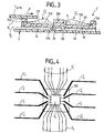
- FIG. 3 illustrates, in section, an example of a connector 1 ′ according to a another embodiment. This figure highlights the hardware configuration body 10 of the connector.
- the body 10 of the connector 1 ′ is conventionally supported by a printed circuit 4 on which the electronics of the reader device are installed (not shown). Facing upwards (in the example illustrated), it comprises two cavities, 100 and 101, located on either side of a central elevation 103.
- the brush contact elements are arranged , for example C " 2 and C" 6 , or more exactly the upper parts, 23 and 63, respectively, thereof.
- the brush contact elements have an elongated shape and are folded back on themselves so as to be embedded in determined zones of the body 10 of the connector 1 ′ and that they open into an internal cavity 105, containing the integrated circuit I C.
- This arrangement advantageously makes it possible to directly connect the appropriate inputs-outputs of the integrated circuit IC to the brush contact elements, without passing through intermediate contacts (such as C ′ 1 or C ′ 5 in FIG. 2).
- the set defines a frame on which the C arte card slides when it is inserted in the reader (arrow f).
- the central elevation 103 advantageously has the same height h as the lateral flanges to facilitate guiding the card C.
- the non-free ends of the brush contact elements, C " 2 and C" 6 are embedded in these lateral flanges, 102 and 104, which lock them in a slightly inclined upward position, relative to the plane P 1 . Consequently, due to the elasticity of the material composing them, the free parts of the contacts play the role of springs rubbing on the underside of the card, which includes the contact areas of the microcircuit (not shown).
- the brushes are folded, as indicated above. They then sink in a substantially vertical direction (in the figure) and are folded a second time (plane P 2 ) in order to be able to end up in the central cavity 105: parts 24 and 64.
- FIG. 4 more particularly illustrates the wiring of the integrated circuit I C. This is shown in its cavity 105, seen from above with respect to FIG. 3.
- the brushes all end up in this cavity 105, on the left side, for the brushes C “ 1 to C” 4 , and on the right, for the brushes C " 5 to C” 8 , and they are connected to the I / O of the integrated circuit I C.
- two bundles of contact elements S i and S ' i , respectively, also connected to inputs-outputs of the integrated circuit I C.
- These contact elements play a role similar to the contact elements S 1 to S 11 of FIG. 2. They are connected, via the printed circuit 4, to the electronic circuits of the reader (not shown).
- FIG. 5a illustrates another embodiment of a 1 "connector according to the invention.
- the zone 105 ′ in which the integrated circuit is located (I C ) is offset laterally with respect to the pairs of contacts C 1 to C 8
- the contact pads to be connected to the inputs / outputs of the integrated circuit I C are located in a plane coincident with the plane P 2 , as defined above. They are connected, as described, either directly to the electronic circuits of the reader, or to the pair of limit switches C fc1 -C fc2 , or to the ground and to the corresponding brush C 5 , or again to the brush d power supply C 1 (and possibly to certain signal brushes in an exemplary embodiment not described).
- the bundle of direct links with the electronic circuits of the reader is identified under the general reference f Si .
- the ground link to the reader is labeled S ' 5 .
- the rear ends, 82 'to 84' and 86 'to 88', of the signal brushes (not connected to the inputs / outputs of the integrated circuit), C 2 to C 4 and C 6 to C 8 are raised and bent in the form of "S" flattened, so as to be flush in a plane P 3 situated at a higher level (in FIG. 5a) at the level of the plane P 2 . It is the same for the ends of the bundle of connections f Si which are flush with the plane P 3 , as well as the end of S ' 5 (ground connection).
- the ends of the supply brushes, C 1 , and of the ground brushes, C 5 are raised and curved but are substantially flush with the plane P 2 .
- This arrangement makes it possible to connect the appropriate pads of the circuit IC by means of conductive strips, CS 1 and CS 5 , respectively, to the brushes C 1 and C 5 . These blades are included in the plane P 2 .
- FIG. 5b illustrates, in partial section, in more detail, the arrangement of the brushes and blades CS 1 and CS 2 mentioned above in the body 10 "of the connector 1".
- the fragment illustrated shows the three brushes C1, C2 and C3 as well as the conductive strip CS 1 .
- the latter is arranged in a groove 106 ", orthogonal to the blades constituting the brushes. It can be seen that the ends 82 'and 83' are flush with the plane P 3 , while the end 81 'is just below the plane P 2 , so as to be connected with the CS 1 blade.
- the flexible blades forming the brushes are located substantially in the plane P 1 , over most of their length.
- the circuit I C provides the interface between at least part of the contact elements (brushes, "limit switch” contacts, etc.) usually used in connectors of Art Connu and l reader electronics.
- the management of the functions related to the control of the insertion, removal and correct positioning of the card C is “transparent” for this electronics. It suffices in particular to provide, via the contact elements S 1 to S 11 , the supply of electrical energy to the microcircuit of the card, which also serves to supply the integrated circuit I C.
- the main advantage is that the designer of a particular application, using a card reader, is relieved of the above management. He just has to select a connector, possibly of a particular model, offering such or such functionalities, in as an active component.
- the invention applies in many fields: cards bank or credit, phone card, "electronic wallet”, toll, staff pointing, access card (security), etc.
Abstract
Description
L'invention concerne un connecteur pour appareil lecteur de carte à microcircuit.The invention relates to a connector for a card reader device. microcircuit.
L'invention concerne également un appareil lecteur de carte à microcircuit comprenant un tel connecteur.The invention also relates to a card reader device with microcircuit comprising such a connector.
Dans le cadre de l'invention, on entend par "carte" toutes les cartes comportant un circuit intégré monolithique ou hybride, dit "puce". Il s'agit, par exemple, de carte du format "carte de crédit", connue encore sous la dénomination "CAM" (Carte A Mémoire"). Le plus souvent, le microcircuit de la carte comprend un microprocesseur ou un microcontrôleur, comportant, notamment des circuits de mémoire, par exemple de type "PROM". Ce type de carte est destiné à être inséré dans des dispositifs spécifiques de lecture et/écriture de données. Pour simplifier, ces dispositifs seront appelés "lecteurs" dans ce qui suit, étant bien entendu qu'il peut également assurer l'écriture de données et d'autres fonctions annexes (alimentation en énergie électrique, tests, etc...) Les données sont stockées dans les circuits mémoires précités, généralement sous forme cryptée. Elles sont donc lues à partir de positions mémoires ou au contraires écrites dans ces positions mémoires.In the context of the invention, the term "card" means all the cards comprising a monolithic or hybrid integrated circuit, called "chip". This is, by example, a card in the "credit card" format, also known under the name "CAM" (Memory Card "). Most often, the microcircuit on the card includes a microprocessor or a microcontroller, comprising, in particular circuits for memory, for example of the "PROM" type. This type of card is intended to be inserted in specific data reading and / or writing devices. To simplify, these devices will be called "readers" in the following, it being understood that can also write data and other related functions (power supply, tests, etc.) The data is stored in the aforementioned memory circuits, generally in encrypted form. They are therefore read at from memory positions or on the contrary written in these memory positions.
Dans tous les cas, il existe des organes d'entrée-sortie constitués par des plages de contact affleurant en surface d'une des faces principales de la carte. Diverses normes définissent la position de ces plages de contact. Ils servent, non seulement pour les entrées-sorties de données précitées, mais aussi pour l'alimentation en énergie électrique du microcircuit ainsi que pour effectuer diverses vérifications, selon les applications considérées (test de présence, etc.). Le lecteur comporte des contacts balais qui viennent en contact galvanique avec les plages précitées, lorsque la carte est correctement insérée dans un connecteur prévu à cet effet.In all cases, there are input-output members constituted by contact pads flush with the surface of one of the main faces of the card. Various standards define the position of these contact pads. They serve, no only for the above-mentioned data inputs and outputs, but also for the supply of electrical energy to the microcircuit as well as for carrying out various verifications, depending on the applications considered (presence test, etc.). The reader includes brush contacts which come into galvanic contact with the pads above, when the card is correctly inserted in a connector provided for this effect.
Dans cette application un certain nombre de problèmes doivent être
résolus simultanément, dont les suivants :
Dans tous ces cas, il est nécessaire de bloquer le fonctionnement du lecteur et couper l'alimentation en énergie électrique pour limiter les risques de détérioration des circuits et/ou tentatives de fraude.In all these cases, it is necessary to block the operation of the drive and cut off the power supply to limit the risk of deterioration of circuits and / or fraud attempts.
Il existe de nombreux systèmes de lecteurs visant à résoudre tout ou partie de ces problèmes. Il est possible de les classer en trois grandes catégories.There are many reader systems aimed at solving all or part of these problems. It is possible to classify them into three main categories.
La première catégorie est constituée par des systèmes de détection électronique.The first category consists of detection systems electronic.
Dans ce type de systèmes, avant d'envoyer une tension électrique au microcircuit, on procède à un test électrique, par exemple la mesure de la résistance entre les contacts balais. Si ces tests ne correspondent pas à des valeurs prévues, dans une gamme donnée, il en est déduit que la carte est mal insérée ou qu'un objet étranger est introduit à sa place.In this type of system, before sending an electrical voltage to the microcircuit, an electrical test is carried out, for example the resistance measurement between the brush contacts. If these tests do not match expected values, in a given range, it is deduced from this that the card is inserted incorrectly or that an object stranger is introduced in his place.
Ce type de système comporte plusieurs inconvénients et parmi lesquels, les suivants :
- Le système devrait fonctionner pour tous les types de microcircuits dont sont équipées les cartes du marché, du moins pour une application donnée (cartes bancaires, etc.). Or la variété de microcircuits est trop importante pour permettre une procédure simple et unique.
- La détection s'effectue juste au passage entre une zone interdite et une zone de fonctionnement. Il est aisé de comprendre, qu'en cas d'arrachement, le système doit réagir très rapidement. L'électronique appropriée à cette fonction est complexe et donc coûteuse.
- The system should work for all types of microcircuits with which market cards are fitted, at least for a given application (bank cards, etc.). However, the variety of microcircuits is too great to allow a simple and unique procedure.
- Detection is carried out just at the passage between a prohibited zone and an operating zone. It is easy to understand that in the event of a wrench, the system must react very quickly. The appropriate electronics for this function are complex and therefore expensive.
La deuxième catégorie est constituée par des systèmes dits "à atterrissage". Un exemple d'un tel système est décrit dans la demande de brevet français FR-A-2 628 901. The second category consists of so-called "to landing ". An example of such a system is described in the patent application French FR-A-2 628 901.
Conformément à ces systèmes, la carte est positionnée contre une butée avant mise en contact avec les balais. Le contact s'effectue par déplacement relatif de la carte vers les balais, perpendiculairement à la surface de la carte (faces principales).According to these systems, the card is positioned against a stop before contacting the brushes. Contact is made by relative displacement from the card to the brushes, perpendicular to the surface of the card (faces main).
La sécurité peut n'être assurée que par le bon fonctionnement des organes mécaniques du système. On peut cependant les doubler par un contact type "fin de course" qui bloque la séquence de mise sous tension au cas où la carte ne serait pas en position correcte. Un séquencement de la mise sous tension peut être assurée par la hauteur des balais, ou par une initialisation de l'électronique par fermeture d'un contact "présence carte". Un tel système est décrit par exemple dans le brevet européen EP 0 139 593. Ce brevet décrit en effet, un appareil lecteur de carte à microcircuit comprenant:
- un connecteur comportant un corps supportant des éléments de contact balais destinés à être mis en contact électrique avec des plages conductrices associées audit microcircuit de la carte lorsque celle-ci est insérée dans le connecteur; et
- un circuit intégré comportant des moyens pour contrôler des opérations d'insertion ou de retrait de la carte dans le lecteur, ledit circuit étant relié, d'une part, avec au moins une partie desdits éléments de contact balais et, d'autre part, avec le circuit électronique du lecteur de carte.
- a connector comprising a body supporting brush contact elements intended to be brought into electrical contact with conductive pads associated with said microcircuit of the card when the latter is inserted in the connector; and
- an integrated circuit comprising means for controlling operations of inserting or removing the card in the reader, said circuit being connected, on the one hand, with at least part of said brush contact elements and, on the other hand, with the electronic circuit of the card reader.
Le principal inconvénient de ce système est constitué par le fait que l'agencement mécanique nécessaire pour réaliser les fonctions précitées est complexe et coûteux.The main drawback of this system is that the mechanical arrangement necessary to perform the above functions is complex and expensive.
La troisième catégorie est constituée par des systèmes à contact balais frottants avec contact de "fin de course". Un tel système est divulgué, par exemple, par la demande de brevet français FR-A-2 623 314.The third category consists of brush contact systems rubbing with "limit switch" contact. Such a system is disclosed, for example, by French patent application FR-A-2 623 314.
Conformément à ces systèmes, les connecteurs dans lesquels sont insérées les cartes sont munis d'un contact de "fin de course" qui déclenche la mise sous tension du microcircuit lorsque la carte est en position correcte.In accordance with these systems, the connectors in which are cards inserted have a "limit switch" contact which triggers the bet on the microcircuit when the card is in the correct position.
L'agencement mécanique est simple et peu coûteux, cependant il présente au moins l'inconvénient de nécessiter l'incorporation, dans l'électronique du lecteur, de circuits de gestion du contact "fin de course" précité.The mechanical arrangement is simple and inexpensive, however it has at least the disadvantage of requiring the incorporation, in the electronics of the reader, circuits for managing the aforementioned "limit switch" contact.
Des inconvénients sont en outre communs à plusieurs systèmes.Disadvantages are also common to several systems.
Dans le cas des systèmes de détection électronique ou utilisant des contacts "fin de course", des fonctions propres à la gestion de la position de la carte doivent être implémentées dans l'électronique du lecteur, donc être prises en compte dans les études de chaque application.In the case of electronic detection systems or using "limit switch" contacts, functions specific to managing the position of the card must be implemented in the electronics of the reader, so be taken into account in the studies of each application.
Pour des raisons de rapidité de développement et de diminution des coûts, les concepteurs d'appareils lecteurs utilisent le plus souvent des systèmes à microprocesseurs. Ils présentent naturellement une bonne souplesse puisqu'il suffit de modifier le programme lorsque les caractéristiques d'une application donnée évoluent, pour une raison ou une autre. Cependant, comme il est bien connu, une logique programmée est plus lente qu'une logique câblée effectuant les mêmes fonctions.For reasons of rapid development and decrease in costs, the designers of reader devices most often use microprocessors. They naturally have good flexibility since it is sufficient modify the program when the characteristics of a given application evolve, for one reason or another. However, as is well known, a programmed logic is slower than wired logic performing the same functions.
L'invention se fixe pour but d'apporter une solution aux problèmes mentionnés ci-dessus, tout en palliant les inconvénients des systèmes de l'Art Connu.The invention sets itself the goal of providing a solution to the problems mentioned above, while overcoming the disadvantages of Art systems Known.
Suivant l'invention, telle que définie dans la revendication 1, le connecteur pour un appareil lecteur de carte à
microcircuit comportant un corps supportant des éléments de contact balais destinés
à être mis en contact électrique avec des plages conductrices associées audit
microcircuit de la carte lorsque celle-ci est insérée dans le connecteur; au moins une
partie des éléments de contact balais étant reliée à un circuit électronique
comportant des moyens pour contrôler des opérations d'insertion ou de retrait de la
carte dans le lecteur, ledit circuit étant relié, d'autre part, avec le circuit électronique
du lecteur de carte; ledit connecteur étant caractérisé en ce qu'il comprend et porte
ledit circuit électronique.According to the invention, as defined in
L'invention a encore pour objet un appareil lecteur de carte comprenant un tel connecteur.The invention also relates to a card reader device comprising such a connector.
Ainsi, le connecteur selon l'invention porte lui-même et non pas le lecteur, un circuit électronique qui permet de contrôler les différentes opérations d'insertion ou de retrait de la carte dans le lecteur de carte.Thus, the connector according to the invention carries itself and not the reader, an electronic circuit which makes it possible to control the various operations inserting or removing the card in the card reader.
De ce fait, on simplifie la construction du lecteur de carte. Ce dernier peut être connecté à différents connecteurs comprenant chacun un circuit électronique intégré apte à contrôler l'insertion de cartes à microcircuit de différentes natures.As a result, the construction of the card reader is simplified. This last can be connected to different connectors each comprising a circuit integrated electronics capable of controlling the insertion of microcircuit cards different natures.
L'invention sera mieux comprise et d'autres caractéristiques et avantages apparaítront à la lecture de la description qui suit en référence aux figures annexées, et parmi lesquelles:
- La figure 1 représente en perspective un connecteur selon l'invention, une carte à puce et schématiquement le circuit électronique avec lequel le connecteur est destiné à être relié,
- La figure 2 illustre schématiquement en éclaté, un exemple de connecteur pour appareil lecteur de carte à microcircuit,
- La figure 3 illustre schématiquement, en coupe longitudinale, un exemple de connecteur pour appareil lecteur de carte à microcircuit, selon un autre mode de réalisation de l'invention;
- La Figure 4 illustre, vue de haut, la disposition d'un circuit intégré spécifique utilisé dans cet autre mode de réalisation de connecteur selon l'invention.
- La figure 5a illustre schématiquement, en éclaté, un exemple de connecteur pour appareil lecteur de carte à microcircuit, selon le mode de réalisation de l'invention représenté à la figure 1;
- La figure 5b illustre une vue partielle en coupe de ce connecteur.
- FIG. 1 shows in perspective a connector according to the invention, a smart card and schematically the electronic circuit with which the connector is intended to be connected,
- FIG. 2 schematically illustrates an exploded view, an example of a connector for a microcircuit card reader device,
- FIG. 3 schematically illustrates, in longitudinal section, an example of a connector for a microcircuit card reader device, according to another embodiment of the invention;
- Figure 4 illustrates, seen from above, the arrangement of a specific integrated circuit used in this other embodiment of the connector according to the invention.
- FIG. 5a schematically illustrates, in exploded view, an example of a connector for a microcircuit card reader device, according to the embodiment of the invention shown in FIG. 1;
- Figure 5b illustrates a partial sectional view of this connector.
Dans la réalisation de la figure 1, le connecteur 1 pour appareil lecteur
de carte C à microcircuit 3 comporte un corps 2 supportant des éléments de contacts
balais C1 à C8, destinés à être mis en contact électrique avec des plages conductrices
associées audit microcircuit IC lorsque la carte C est insérée dans le connecteur 1.In the embodiment of FIG. 1, the
Conformément à l'invention, ce connecteur 1 comporte un circuit
électronique IC relié,d'une part, avec au moins une partie desdits éléments de contact
balais C1 à C8 et, d'autre part, avec le circuit électronique 4 du lecteur de carte. Le
circuit électronique IC porté par le connecteur 1 comporte des moyens qui seront
détaillés plus loin pour contrôler des opérations d'insertion ou de retrait de la carte C
dans le lecteur de carte.According to the invention, this
La figure 2 illustre schématiquement, en éclaté, l'agencement d'un
connecteur 1 selon un mode de réalisation particulier de l'invention. Plus
précisément, sur cette figure, on n'a illustré que les dispositions relatives aux
différents éléments de contacts du connecteur.Figure 2 schematically illustrates, in exploded view, the arrangement of a
Selon une caractéristique essentielle de l'invention, on dispose un circuit
intégré IC au sein même du connecteur 1. Plus précisément, le circuit IC est disposé
dans un logement ménagé dans l'épaisseur de l'isolant du cadre du connecteur (non
représenté sur cette figure).According to an essential characteristic of the invention, there is an integrated circuit I C within the
Le connecteur comprend deux jeux d'éléments de contacts.The connector includes two sets of contact elements.
Un premier jeu, situé sensiblement dans un premier plan P1, ou plan
inférieur sur la figure 2, comprend une série de paires de contacts balais ; quatre
paires dans l'exemple illustré, C1 à C8. Ces contacts balais, C1 à C8, sont constitués
de lames flexibles, parallèles entre elles et dont des premières extrémités en vis à
vis, 10 à 80, présentent une courbure et sont destinées à être mises en contact avec
des plages de contacts correspondantes (non représentées) de la carte à microcircuit,
symbolisée par la flèche C, après insertion de celle-ci dans le connecteur 1. Le
premier jeu de contacts comprend également, avantageusement, une paire de
contacts de "fin de course" Cfc1 et Cfc2, respectivement.A first set, located substantially in a first plane P 1 , or lower plane in FIG. 2, comprises a series of pairs of brush contacts; four pairs in the example illustrated, C 1 to C 8 . These brush contacts, C 1 to C 8 , consist of flexible blades, mutually parallel and whose opposite opposite ends, 10 to 80, have a curvature and are intended to be brought into contact with corresponding contact pads. (not shown) of the microcircuit card, symbolized by the arrow C, after insertion of the latter into the
Dans l'exemple illustré, l'allocation des balais est la suivante :
- élément de contact C1 : amenée de la tension d'alimentation ;
- élément de contact C5 : mise à la masse ;
- éléments de contact C2 à C4 et C6 à C8 : contacts balais de "signaux" (entrées et/ou sorties).
- contact element C 1 : supply voltage;
- contact element C 5 : earthing;
- contact elements C 2 to C 4 and C 6 to C 8 : brush contacts of "signals" (inputs and / or outputs).
En soi, ces dispositions sont entièrement communes à l'art connu.In themselves, these provisions are entirely common to known art.
Le connecteur 1 comprend un second jeu d'élément de contacts, C'1 à
C'8, C'fc1-C'fc2 et S1 à S11, disposés dans un second plan P2, supérieur sur la figure
et sensiblement parallèle au premier. Ce jeu d'éléments de contacts, C'1 à C'8, C'fc1-C'fc2
et S1 à S11, est connecté entre les éléments de contacts balais, C1 à C8, les
entrées-sorties du microcircuit IC et les circuits électroniques de l'appareil lecteur de
carte à microcircuit (non représenté).The
Le connecteur ci-dessus est généralement monté sur un circuit imprimé supportant l'électronique du lecteur, par exemple par soudage de broches d'entrées-sorties dans des trous métallisés réalisés sur le circuit imprimé. C'est donc par l'intermédiaire de pistes conductrices, connectées, d'une part, aux trous métallisés, et, d'autre part, aux circuits électroniques de l'appareil lecteur, que s'effectuent les liaisons électriques entre le second jeu d'éléments de contacts et ces circuits électroniques.The above connector is usually mounted on a printed circuit supporting reader electronics, for example by welding input-output pins in metallized holes made on the printed circuit. So it's by through conductive tracks, connected, on the one hand, to the metallized holes, and, on the other hand, to the electronic circuits of the reader device, that the electrical connections between the second set of contact elements and these circuits electronic.
Parmi les éléments de contacts du second jeu, on peut distinguer trois types, selon leurs raccordements :
- Une première partie, C'2 à C'8 (dans l'exemple illustré), établit une connexion directe entre les éléments de contact balais du connecteur 1 et l'électronique de l'appareil lecteur, via le circuit imprimé précité. Il s'agit, en général de tout ou partie des éléments de contact balais "signaux" (soit C2 à C4 et C6 à C8) dans l'exemple illustré. Contrairement à ce qui est représenté sur la figure 2, le balai élément de contact "masse" C5, peut éventuellement être connecté de cette manière à l'électronique de l'appareil lecteur.
- Une deuxième partie, C'fc1, C'fc2, C1 (dans l'exemple illustré), établit une connexion entre des éléments de contact balais du connecteur et certaines entrées-sorties du circuit intégré IC. Il s'agit de contacts auxiliaires, généralement les balais éléments de contacts "fin de course", Cfc1 et Cfc2, les balais éléments de contact tension d'alimentation, C1, et éventuellement certains balais éléments de contact "signaux" ou le balais élément de contact "masse" C5.
- Enfin, une troisième partie, S4, S8 à S11, connecte directement des sorties et/ou entrées du circuit intégré IC, aux circuits électroniques de l'appareil lecteur, via le circuit imprimé précité. Un des éléments de contact ci-dessus, véhicule l'alimentation en énergie électrique, qui transite par le circuit intégré IC.
- A first part, C ' 2 to C' 8 (in the example illustrated), establishes a direct connection between the brush contact elements of the
connector 1 and the electronics of the reader device, via the aforementioned printed circuit. These are, in general, all or part of the "signal" brush contact elements (ie C 2 to C 4 and C 6 to C 8 ) in the example illustrated. Contrary to what is shown in FIG. 2, the brush "mass" contact element C 5 , can possibly be connected in this way to the electronics of the reader device. - A second part, C ' fc1 , C' fc2 , C 1 (in the example illustrated), establishes a connection between brush contact elements of the connector and certain inputs-outputs of the integrated circuit I C. These are auxiliary contacts, generally the brushes for "limit switch" contact elements, C fc1 and C fc2 , the brushes for supply voltage contact elements, C 1 , and possibly certain brushes for "signal" contact elements or the brush "mass" contact element C 5 .
- Finally, a third part, S 4 , S 8 to S 11 , directly connects outputs and / or inputs of the integrated circuit I C , to the electronic circuits of the reader device, via the aforementioned printed circuit. One of the above contact elements conveys the supply of electrical energy, which passes through the integrated circuit I C.
Dans la configuration matérielle particulière, représentée sur la figure 2,
pour des raisons de facilité de réalisation du connecteur 1, les éléments de contacts,
C'2 à C'4, C'5 à C'8, du jeu supérieur, sont prolongés par des éléments de contacts
allongés, S3 à S1, S4 à S7, respectivement, sensiblement parallèles entre eux, suivant
une direction orthogonale à la direction des éléments de contacts, C'2 à C'4, C'5 à
C'8.In the particular hardware configuration, shown in FIG. 2, for reasons of ease of making the
Naturellement, quelle que soit la solution retenue pour l'élément balais de "masse" C5, connexion directe ou non, le circuit intégré IC comporte une connexion de masse reliée à la masse, c'est-à-dire à C'5-S4 (dans l'exemple illustré).Naturally, whatever the solution adopted for the “mass” brush element C 5 , direct or not connection, the integrated circuit I C comprises a ground connection connected to ground, that is to say to C ' 5 -S 4 (in the example illustrated).
Pour mieux mettre en évidence la disposition des éléments de contacts des deux jeux, on a éloigné les plans P1 et P2 de façon exagérée. En réalité, les deux jeux sont dans des plans, P1 et P2, faiblement écartés, de manière à ce que les secondes extrémités, 11 à 81, des éléments balais, C1 à C8, opposées premières extrémités 10 à 80, soient mises en contact galvanique avec les extrémités, 12 à 82, en relation de vis à vis, des éléments de contacts correspondants du jeu supérieur, C'1 à C'8. Il en est de même des extrémités en vis à vis des éléments de contacts de "fin de course", Cfc1-Cfc2, d'une part, et C'fc1-C'fc2, d'autre part.To better highlight the arrangement of the contact elements of the two sets, the planes P 1 and P 2 have been removed in an exaggerated manner. In reality, the two sets are in planes, P 1 and P 2 , slightly spaced apart, so that the second ends, 11 to 81, of the brush elements, C 1 to C 8 , opposite the first ends 10 to 80, are brought into galvanic contact with the ends, 12 to 82, in relation to opposite, of the corresponding contact elements of the upper clearance, C ' 1 to C' 8 . The same is true of the opposite ends of the "end-of-travel" contact elements, C fc1 -C fc2 , on the one hand, and C ' fc1 -C' fc2 , on the other hand.
Les extrémités d'éléments de contact en vis à vis peuvent être soudées.The ends of facing contact elements can be welded.
Pour établir les liaisons avec les entrées-sorties du circuit intégré IC, on peut faire appel à la technique classique de soudage de fils.To establish the connections with the inputs-outputs of the integrated circuit I C , it is possible to use the conventional technique of wire welding.
L'étude et la réalisation du circuit intégré sont réalisées en faisant appel également aux techniques de développement classiques de circuits intégrés spécifiques. On englobe sous le terme,"circuit intégré" notamment, aussi bien les circuits intégrés monolithiques que les circuits hybrides.The study and the realization of the integrated circuit are carried out by calling also to the classical development techniques of integrated circuits specific. We include under the term, "integrated circuit" in particular, both monolithic integrated circuits as hybrid circuits.
Les principales fonctions accomplies par le circuit intégré IC sont les suivantes :
- la scrutation de l'état de la paire de contacts "fin de course", Cfc1-Cfc2 ;
- la commande des mises sous et hors tension du microcircuit de la carte Carte, en fonction de l'état précité ; la fonction interrupteur étant intégrée dans le circuit IC ;
- des fonctions de tests éventuels de certaines caractéristiques électriques entre éléments de contact balais : par exemple, la résistance ou l'impédance entre deux éléments de contact balais ou la réponse à un signal impulsionnel;
- l'intégration éventuelle de certaines fonctions standards relatives à la transmission de données.
- scanning the state of the "limit switch" contact pair, C fc1 -C fc2 ;
- the control of power on and off of the microcircuit of the card C arte , according to the aforementioned state; the switch function being integrated in the circuit I C ;
- possible test functions for certain electrical characteristics between brush contact elements: for example, the resistance or impedance between two brush contact elements or the response to a pulse signal;
- the possible integration of certain standard functions relating to data transmission.
Les techniques actuelles d'intégration à large échelle permettent d'intégrer des fonctions supplémentaires, telles que des fonctions relatives à l'exploitation de la carte à microcircuit C.Current large-scale integration techniques allow to integrate additional functions, such as functions relating to the operation of the microcircuit card C.
Il est également possible d'implémenter sur le connecteur 1, à l'aide du
circuit intégré IC, la totalité des fonctions logiques de l'appareil lecteur,
l'électronique extérieure au connecteur se limitant, dans ce cas, aux organes
d'entrées-sorties.It is also possible to implement on the
Il est alors possible de proposer, en tant que composant actif, des connecteurs, de divers modèles, différant essentiellement par les capacités du circuit intégré, exprimées en termes de fonctionnalités, par exemple.It is then possible to propose, as an active component, connectors, of various designs, differing mainly in circuit capabilities integrated, expressed in terms of functionality, for example.
La figure 3 illustre, en coupe, un exemple de connecteur 1' selon un
autre mode de réalisation. Cette figure met en évidence la configuration matérielle
du corps 10 du connecteur.FIG. 3 illustrates, in section, an example of a
. Une seule paire d'éléments balais, C"2-C"6, est visible sur cette figure 3, paire qui correspond fonctionnellement à la paire C2-C6 de la figure 2. Toutefois il existe le même nombre de paires de balais pour un type de carte C donnée. Il en est de même des paires de contacts de "fin de course" (non visibles sur cette figure 3).. Only one pair of brush elements, C " 2 -C" 6 , is visible in this figure 3, a pair which corresponds functionally to the pair C 2 -C 6 of figure 2. However, there are the same number of pairs of brushes for a given type of card C. The same is true for pairs of "limit switch" contacts (not visible in this figure 3).
Le corps 10 du connecteur 1', en matériau électriquement isolant, est
supporté, de façon classique, par-un circuit imprimé 4 sur lequel est implantée
l'électronique de l'appareil lecteur (non représentée). Tournées vers le haut (dans
l'exemple illustré), il comprend deux cavités, 100 et 101, situées de part et d'autre
d'une surélévation centrale 103. On dispose dans ces cavités, 100 et 101, les
éléments de contact balais, par exemple C"2 et C"6, ou plus exactement les parties
supérieures, 23 et 63, respectivement, de ceux-ci. Dans ce mode de réalisation, les
éléments de contact balais ont une forme allongée et sont repliés sur eux-mêmes de
manière à être noyés dans des zones déterminées du corps 10 du connecteur 1' et
qu'ils débouchent dans une cavité interne 105, contenant le circuit intégré IC. Cette
disposition permet, avantageusement, de connecter directement les entrées-sorties
appropriées du circuit intégré IC aux éléments de contact balais, sans passer par des
contacts intermédiaires (tels que C'1 ou C'5 sur la figure 2).The
On peut également faire transiter tous les éléments de contact balais par le circuit intégré IC, même si, fonctionnellement, ce transit n'est nécessaire que pour quelques uns des éléments de contact balais : tension d'alimentation, etc. Il suffit alors de prévoir des liaisons internes appropriées. It is also possible to pass all the brush contact elements through the integrated circuit I C , even if, functionally, this transit is only necessary for some of the brush contact elements: supply voltage, etc. It then suffices to provide appropriate internal links.
Des rebords latéraux, 102 et 104, bordent les cavités 101 et 100,
respectivement. L'ensemble définit un cadre sur lequel glisse la carte Carte
lorsqu'elle est introduite dans le lecteur (flèche f). La surélévation centrale 103
présente avantageusement de la même hauteur h que les rebords latéraux pour
faciliter le guidage de la carte C. Les extrémités non libres des éléments de contact
balais, C"2 et C"6, sont noyées dans ces rebords latéraux, 102 et 104, qui les
verrouillent en position légèrement inclinée vers le haut, par rapport au plan P1. En
conséquence, en raison de l'élasticité du matériau les composant, les parties libres
des contacts jouent le rôle de ressorts frottant sur la face inférieure de la carte, qui
comporte les plages de contacts du microcircuit (non représentées). C'est dans
l'épaisseur des rebords latéraux que les balais sont repliés, comme il a été indiqué
précédemment. Ils s'enfoncent alors selon une direction sensiblement verticale (sur
la figure) et sont repliés une seconde fois (plan P2) pour pouvoir aboutir dans la
cavité centrale 105 : parties 24 et 64.Side edges, 102 and 104, line the
La figure 4 illustre plus particulièrement le câblage du circuit intégré IC.
Celui-ci est représenté dans sa cavité 105, vu de haut par rapport à la figure 3. Dans
cet exemple, les balais aboutissent tous dans cette cavité 105, sur la partie gauche,
pour les balais C"1 à C"4, et sur la partie droite, pour les balais C"5 à C"8, et ils sont
connectés à des entrées-sorties du circuit intégré IC.FIG. 4 more particularly illustrates the wiring of the integrated circuit I C. This is shown in its
On a également représenté, sur les parties basse et haute de la figure 4,
deux faisceaux d'éléments de contacts, Si et S'i, respectivement, également
connectés à des entrées-sorties du circuit intégré IC. Ces éléments de contact jouent
un rôle similaire aux éléments de contacts S1 à S11 de la figure 2. Ils sont connectés,
via le circuit imprimé 4, aux circuits électroniques du lecteur (non représentés).Also shown, on the lower and upper parts of FIG. 4, two bundles of contact elements, S i and S ' i , respectively, also connected to inputs-outputs of the integrated circuit I C. These contact elements play a role similar to the contact elements S 1 to S 11 of FIG. 2. They are connected, via the printed
Dans ce qui précède, on a supposé que la puce de semi-conducteur IC.
était "nue", les éléments de contacts remplaçant les broches d'entrée-sortie. Cela
suppose également que, une fois les connexions réalisées entre les éléments de
contact et les entrées-sorties de la puce IC, il est nécessaire de procéder à des
opérations d'encapsulation spécifiques, de manière à protéger la puce. On peut aussi,
en tant qu'alternative, monter la puce dans un boítier "ISO" standard, puis installer
ce boítier dans la cavité 105 du corps 10 du connecteur 1'. Cette disposition permet
d'éviter les opérations de connexion et d'encapsulation spécifiques.In the foregoing, it has been assumed that the semiconductor chip I C. was "naked", the contact elements replacing the input-output pins. This also assumes that, once the connections have been made between the contact elements and the input-output of the chip I C , it is necessary to carry out specific encapsulation operations, so as to protect the chip. One can also, as an alternative, mount the chip in a standard "ISO" box, then install this box in the
La figure 5a illustre un autre mode de réalisation d'un connecteur 1" selon l'invention.FIG. 5a illustrates another embodiment of a 1 "connector according to the invention.
Dans ce mode de réalisation la zone 105' dans laquelle se trouve le
circuit intégré (IC) est déportée latéralement par rapport aux paires de contacts C1 à
C8 Cette disposition permet, comme on va le montrer, de n'utiliser qu'un seul cadre
de montage. Les plages de contacts à connecter aux entrées/sorties du circuit intégré
IC sont situées dans un plan confondu avec le plan P2, tel que défini précédemment.
Elles sont reliées, comme il a été décrit, soit directement aux circuits électroniques
du lecteur, soit à la paire de contacts de fin de course Cfc1-Cfc2, soit à la masse et
au balai correspondant C5, soit encore au balai d'alimentation C1 (et éventuellement
à certains balais de signaux dans un exemple de réalisation non décrit). Le faisceau
de liaisons directes avec les circuits électroniques du lecteur est repéré sous la
référence générale fSi. La liaison de masse vers le lecteur porte la référence S'5. Les
extrémités arrières, 82' à 84' et 86' à 88', des balais de signaux (non connectés aux
entrées/sorties du circuit intégré), C2 à C4 et C6 à C8 sont relevées et courbées en
forme de "S" aplati, de manière à affleurer dans un plan P3 situé à un niveau
supérieur (sur la figure 5a) au niveau du plan P2. Il en est de même des extrémités
du faisceau de connexions fSi qui affleurent au niveau du plan P3, ainsi que de
l'extrémité de S'5 (connexion de masse). Par contre les extrémités des balais
d'alimentation, C1, et de masse, C5, sont relevées et courbées mais affleurent
sensiblement au niveau du plan P2. Cette disposition permet de connecter les plages
appropriées du circuit IC par l'intermédiaire de lames conductrices, CS1 et CS5,
respectivement, aux balais C1 et C5. Ces lames sont comprises dans le plan P2.In this embodiment, the
La figure 5b illustre,- en coupe partielle, de façon plus détaillée,
l'agencement des balais et des lames CS1 et CS2 précitées dans le corps 10" du
connecteur 1". Le fragment illustré montre les trois balais C1, C2 et C3 ainsi que la
lame conductrice CS1. Cette dernière est disposée dans une rainure 106",
orthogonale aux lames constituant les balais. On constate que les extrémités 82' et
83' affleurent au niveau du plan P3, alors que l'extrémité 81' est juste en dessous du
plan P2, de manière à être connectée avec la lame CS1.FIG. 5b illustrates, in partial section, in more detail, the arrangement of the brushes and blades CS 1 and CS 2 mentioned above in the
On peut donc souder directement (dans le plan P3) toutes les extrémités des connexions du faisceau fSi, la connexion de masse S'5 et toutes les extrémités des balais "signaux", c'est-à-dire les balais non directement reliés aux entrées-sorties du circuit intégré, ou encore aux plages de contact du circuit IC.. On a supposé que les signaux générés par la paire de contacts de "fin de course" Cfc1-Cfc2 transitaient par le circuit intégré pour y être traités. Les extrémités de cette paire de contact affleurent donc également sensiblement au niveau du plan P2, pour être connectées à deux plages de contact du circuit IC.It is therefore possible to directly weld (in the plane P 3 ) all the ends of the connections of the beam f Si , the ground connection S ' 5 and all the ends of the "signal" brushes, that is to say the brushes not directly connected to the I / O of the integrated circuit, or to the contact pads of the I C circuit. It was assumed that the signals generated by the pair of "limit switch" contacts C fc1 -C fc2 passed through the integrated circuit to be treated there. The ends of this contact pair are therefore also flush with the plane P 2 , to be connected to two contact pads of the circuit I C.
Comme précédemment, les lames souples formant les balais sont situées sensiblement dans le plan P1, sur la plus grande partie de leur longueur. As before, the flexible blades forming the brushes are located substantially in the plane P 1 , over most of their length.
La description ci-dessus montre que le circuit IC assure l'interface entre au moins une partie des éléments de contact (balais, contacts de "fin de course", etc.) habituellement utilisés dans les connecteurs de l'Art Connu et l'électronique du lecteur. En d'autres termes, la gestion des fonctions liées au contrôle de l'introduction, du retrait et du positionnement correct de la carte C est "transparente" pour cette électronique. Il suffit notamment de fournir, via les éléments de contacts S1 à S11, l'alimentation en énergie électrique du microcircuit de la carte, qui sert également à alimenter le circuit intégré IC. Une fois la carte C correctement introduite, ou de façon plus générale, lorsque les règle de fonctionnement normal sont respectées (hors condition "d'arrachage", de tentative de fraude, etc.), les circuits électroniques du lecteur envoient et/ou reçoivent les signaux habituels à ce type d'application.The above description shows that the circuit I C provides the interface between at least part of the contact elements (brushes, "limit switch" contacts, etc.) usually used in connectors of Art Connu and l reader electronics. In other words, the management of the functions related to the control of the insertion, removal and correct positioning of the card C is "transparent" for this electronics. It suffices in particular to provide, via the contact elements S 1 to S 11 , the supply of electrical energy to the microcircuit of the card, which also serves to supply the integrated circuit I C. Once the card C has been correctly inserted, or more generally, when the normal operating rules are respected (except for the "tear-off" condition, attempted fraud, etc.), the electronic circuits of the reader send and / or receive the usual signals for this type of application.
Le principal avantage, parmi les autres précédemment énoncés, est que le concepteur d'une application particulière, utilisant un lecteur de carte, est déchargé de la gestion précitée. Il lui suffit de sélectionner un connecteur, éventuellement d'un modèle particulier, offrant telles ou telles fonctionnalités, en tant que composant actif.The main advantage, among the others previously stated, is that the designer of a particular application, using a card reader, is relieved of the above management. He just has to select a connector, possibly of a particular model, offering such or such functionalities, in as an active component.
Bien entendu, l'invention n'est pas limitée aux exemples et aux applications que l'on vient de décrire et on peut y apporter de nombreuses modifications sans sortir du cadre de l'invention.Of course, the invention is not limited to the examples and to the applications that we have just described and we can bring many modifications without departing from the scope of the invention.
Ainsi, l'invention s'applique dans de nombreux domaines : cartes bancaires ou de crédit, carte de téléphone, "porte-monnaie électronique", péage, pointage de personnels, carte d'accès (sécurité), etc.Thus, the invention applies in many fields: cards bank or credit, phone card, "electronic wallet", toll, staff pointing, access card (security), etc.
Claims (10)
- Connector (1) for an apparatus for reading a smart card (C), which comprises a body (2) supporting brush contact elements (C1 to C8) intended to be brought into electrical contact with conducting areas (3) associated with the said microcircuit of the card (C) when the latter is inserted into the connector (1), at least part of the brush contact elements (C1 to C8) being connected to an electronic circuit (IC) which includes means for controlling the operations of inserting the card (C) into the reader or for removing it therefrom, the said circuit (IC) being connected, moreover, to the electronic circuit (4) of the card reader, the said connector being characterized in that it comprises and carries the said electronic circuit (IC).
- Connector according to Claim 1, characterized in that it includes additional contact elements (S1 to S11) intended to be connected to the electronic circuit (4) of the reader, the electronic circuit (IC) carried by the body of the connector being connected to at least part of the said additional contact elements (S1 to S11).
- Connector according to either of Claims 1 and 2, characterized in that the said electronic circuit is an integrated circuit chip and in that input/output pads on the said chip (IC) are connected directly to elements of the said brush contacts (C1, C5) and input/output pads on the said chip (IC) are connected directly to elements of the said additional contacts (S8 to S11), via a second end.
- Connector according to Claim 3, characterized in that furthermore at least some of the said brush contact elements (C2 to C4, C5 to C8) are connected directly to at least some of the said additional contact elements (S1 to S7), via a second end, without passing through input/output pads on the said chip (IC).
- Connector according to any one of the preceding claims, characterized in that it furthermore comprises "end of travel"-detection contact elements (Cfc1 - Cfc2) so as to detect correct insertion of the card (Card) into the connector (1).
- Connector according to Claim 5, characterized in that the said "end of travel"-detection contact elements (Cfc1 - Cfc2) are connected to additional contact elements which are themselves connected directly to input/output pads on the said chip (IC) so that the state of these "end of travel"-detection contact elements (Cfc1 - Cfc2) is controlled by the said electronic circuit (IC).
- Connector according to Claim 6, characterized in that one of the said brush contact elements (C1) is intended to convey the supply of electrical energy for the said microcircuit and the said electronic circuit (IC) receives the energy supply via one of the said additional contact elements, in that it includes an integrated switching function and in that the element is effectively supplied, under the control of the said integrated switching function, when the electronic circuit (IC) detects a state of the said "end of travel"-detection contact elements (Cfc1 - Cfc2) indicating that the card (C) is correctly inserted and blocking this supply in the opposite case, so as to control the switching-on and switching-off of the microcircuit of the said card (C).
- Connector according to one of Claims 1 to 7, characterized in that the said body (10) is trade of an electrically insulating material and includes two open cavities (100, 101), in which the said brush contact elements (C"1 to C"8) are placed, and rims (102, 104) which form a frame guiding the said card (C) during its insertion.
- Connector according to Claim 8, characterized in that the said brush contact elements (C"1 to C"8) each comprise a blade (23, 63) forming a spring in the region covering the said cavities (100, 101) so as to rub against the said conducting areas carried by the said microcircuit when the card (C) is inserted into the connector (1'), these blades being held captive in the said rims and being extended by bent-over parts (24, 64), which emerge in a cavity in the body in which the integrated circuit chip (Ic) is housed, in order to be connected to input/output pads on this chip.
- Apparatus for reading a smart card (C), characterized in that it comprises a connector according to any one of the preceding claims.
Applications Claiming Priority (3)
| Application Number | Priority Date | Filing Date | Title |
|---|---|---|---|
| FR9501271 | 1995-02-03 | ||
| FR9501271A FR2730328B1 (en) | 1995-02-03 | 1995-02-03 | CONNECTOR FOR MICROCIRCUIT CARD READING APPARATUS AND MICROCIRCUIT CARD READING APPARATUS INCLUDING SAME |
| PCT/FR1996/000156 WO1996024111A1 (en) | 1995-02-03 | 1996-01-30 | Connector for a smart card reader apparatus and card reader comprising same |
Publications (2)
| Publication Number | Publication Date |
|---|---|
| EP0807295A1 EP0807295A1 (en) | 1997-11-19 |
| EP0807295B1 true EP0807295B1 (en) | 1998-10-21 |
Family
ID=9475817
Family Applications (1)
| Application Number | Title | Priority Date | Filing Date |
|---|---|---|---|
| EP96902309A Expired - Lifetime EP0807295B1 (en) | 1995-02-03 | 1996-01-30 | Connector for a smart card reader apparatus and card reader comprising same |
Country Status (13)
| Country | Link |
|---|---|
| US (1) | US6165021A (en) |
| EP (1) | EP0807295B1 (en) |
| JP (1) | JPH11500549A (en) |
| KR (1) | KR100420883B1 (en) |
| CN (1) | CN1173232A (en) |
| AT (1) | ATE172563T1 (en) |
| AU (1) | AU701547B2 (en) |
| CA (1) | CA2211344A1 (en) |
| DE (1) | DE69600834T2 (en) |
| ES (1) | ES2125096T3 (en) |
| FR (1) | FR2730328B1 (en) |
| RU (1) | RU2181908C2 (en) |
| WO (1) | WO1996024111A1 (en) |
Families Citing this family (18)
| Publication number | Priority date | Publication date | Assignee | Title |
|---|---|---|---|---|
| FR2743170B1 (en) * | 1995-12-28 | 1998-02-06 | Framatome Connectors Int | ACTIVE CONNECTOR FOR CHIP CARD |
| FI991002A (en) * | 1999-05-03 | 2000-11-04 | Nokia Mobile Phones Ltd | Active card adapter and telecommunicator |
| DE19935188C2 (en) * | 1999-07-27 | 2002-06-13 | Amphenol Tuchel Elect | Contact block for a chip card reader |
| US6942154B1 (en) * | 2000-02-24 | 2005-09-13 | Matsushita Electric Industrial Co, Ltd. | Card connector and portable telephone having the same |
| FR2805671B1 (en) * | 2000-02-25 | 2002-07-26 | Sagem | CONNECTOR FOR CHIP CARDS |
| US6769036B1 (en) * | 2000-05-16 | 2004-07-27 | Palm Source, Inc. | Method and system for enabling personal digital assistants and protecting stored private data |
| US6856595B1 (en) * | 2000-05-19 | 2005-02-15 | Mosaid Technologies, Inc. | Method and apparatus for providing input back pressure in an output buffered switch |
| US7344074B2 (en) * | 2002-04-08 | 2008-03-18 | Nokia Corporation | Mobile terminal featuring smart card interrupt |
| TW555110U (en) * | 2002-08-28 | 2003-09-21 | Carry Computer Eng Co Ltd | Adapter for xD memory card |
| WO2004029858A1 (en) * | 2002-09-25 | 2004-04-08 | Koninklijke Philips Electronics N.V. | Connector for chip-card |
| WO2006057049A1 (en) * | 2004-11-26 | 2006-06-01 | Kabushiki Kaisha Toshiba | Card and host device |
| CN100583121C (en) * | 2005-03-30 | 2010-01-20 | Nxp股份有限公司 | A portable object connectable package |
| TWM308521U (en) * | 2006-09-26 | 2007-03-21 | Jess Link Products Co Ltd | Adapter card structure |
| US8061609B2 (en) * | 2007-05-14 | 2011-11-22 | Sony Ericsson Mobile Communications Ab | Space efficient card readers and electronic devices incorporating same |
| CN101242047B (en) | 2008-02-26 | 2010-06-09 | 华为终端有限公司 | USB connection member and USB device |
| ES2413164R1 (en) * | 2011-10-10 | 2013-10-10 | Televes Sa | CHEST FOR ELECTRONIC EQUIPMENT WITH CONNECTION SYSTEM FOR PRINTED CIRCUIT PLATE |
| CN106033850B (en) | 2015-03-13 | 2019-01-04 | 小米科技有限责任公司 | Smart card deck and electronic equipment |
| CN113723122A (en) * | 2021-08-30 | 2021-11-30 | 百富计算机技术(深圳)有限公司 | Card reading circuit, card reader and card reading system |
Family Cites Families (7)
| Publication number | Priority date | Publication date | Assignee | Title |
|---|---|---|---|---|
| FR2554260B1 (en) * | 1983-10-27 | 1987-10-30 | Flonic Sa | ELECTRONIC MEMORY CARD READING APPARATUS |
| FR2623313B1 (en) * | 1987-11-13 | 1991-10-04 | Cit Alcatel | CONTACT FRAME FOR CHIP CARD READER |
| GB2214680B (en) * | 1988-01-19 | 1991-07-31 | Technophone Ltd | Card reader |
| JPH0255355U (en) * | 1988-10-11 | 1990-04-20 | ||
| FR2668627A1 (en) * | 1990-10-25 | 1992-04-30 | Cit Alcatel | CONTACT FRAME FOR CARD READER. |
| US5161992A (en) * | 1992-01-17 | 1992-11-10 | Amp Incorporated | Electrical connector assembly for a card containing an integrated circuit chip |
| RU2150745C1 (en) * | 1995-03-22 | 2000-06-10 | Фраматом Коннектор Энтернасьональ | Device for reading card with embedded chip |
-
1995
- 1995-02-03 FR FR9501271A patent/FR2730328B1/en not_active Expired - Fee Related
-
1996
- 1996-01-30 DE DE69600834T patent/DE69600834T2/en not_active Expired - Fee Related
- 1996-01-30 ES ES96902309T patent/ES2125096T3/en not_active Expired - Lifetime
- 1996-01-30 CA CA002211344A patent/CA2211344A1/en not_active Abandoned
- 1996-01-30 RU RU97114852/09A patent/RU2181908C2/en not_active IP Right Cessation
- 1996-01-30 EP EP96902309A patent/EP0807295B1/en not_active Expired - Lifetime
- 1996-01-30 AU AU46672/96A patent/AU701547B2/en not_active Ceased
- 1996-01-30 WO PCT/FR1996/000156 patent/WO1996024111A1/en active IP Right Grant
- 1996-01-30 US US08/875,694 patent/US6165021A/en not_active Expired - Fee Related
- 1996-01-30 CN CN96191765A patent/CN1173232A/en active Pending
- 1996-01-30 AT AT96902309T patent/ATE172563T1/en not_active IP Right Cessation
- 1996-01-30 JP JP8523312A patent/JPH11500549A/en active Pending
- 1996-01-30 KR KR1019970705297A patent/KR100420883B1/en not_active IP Right Cessation
Also Published As
| Publication number | Publication date |
|---|---|
| CA2211344A1 (en) | 1996-08-08 |
| ATE172563T1 (en) | 1998-11-15 |
| KR19980701900A (en) | 1998-06-25 |
| AU4667296A (en) | 1996-08-21 |
| RU2181908C2 (en) | 2002-04-27 |
| FR2730328B1 (en) | 1997-04-04 |
| EP0807295A1 (en) | 1997-11-19 |
| US6165021A (en) | 2000-12-26 |
| CN1173232A (en) | 1998-02-11 |
| FR2730328A1 (en) | 1996-08-09 |
| DE69600834D1 (en) | 1998-11-26 |
| JPH11500549A (en) | 1999-01-12 |
| DE69600834T2 (en) | 1999-04-15 |
| WO1996024111A1 (en) | 1996-08-08 |
| ES2125096T3 (en) | 1999-02-16 |
| AU701547B2 (en) | 1999-01-28 |
| KR100420883B1 (en) | 2004-05-20 |
Similar Documents
| Publication | Publication Date | Title |
|---|---|---|
| EP0807295B1 (en) | Connector for a smart card reader apparatus and card reader comprising same | |
| EP0815528B1 (en) | Reading frame for a smart card reader apparatus | |
| EP0343030B1 (en) | Flexible printed circuit, particularly for electronic microcircuit cards, and card incorporating this circuit | |
| EP0139593B1 (en) | Reading apparatus for electronic memory cards | |
| EP0262036B2 (en) | Data processing system with memory cards having a plurality of electronic modules | |
| EP0696010B2 (en) | Portable interface for electronic chip card | |
| EP0274288B1 (en) | Connection unit for electronic memory cards, and reading/writing device using the same | |
| EP0323347B1 (en) | Reading/writing device for memory cards with an anti-fraud device | |
| EP0819283B1 (en) | Data collection system for card readers | |
| FR2554262A1 (en) | Anti-fraud device for electronic-memory card reader | |
| FR2808608A1 (en) | ELECTRONIC MEMORY CARD INTENDED TO BE INTRODUCED INTO A PROCESSING DEVICE | |
| EP0338900A1 (en) | Device for electrical contacting of conductors distributed over two elements and particularly between those of a memory card and those of its reader | |
| CA2212951C (en) | Connector for an apparatus for reading smart cards | |
| EP1659492B1 (en) | Stand-alone electronic device, in particular an ambulatory medical recorder, with a reprogrammable microcontroller | |
| CA2224484C (en) | Removable card with a plug-in connector forming a smart card reader for a microcomputer | |
| EP2790124B1 (en) | Secured connector | |
| EP1045338B1 (en) | Electronic memory card with card security element | |
| FR2619941A1 (en) | System for controlling the link between two terminals of a data processing installation | |
| FR2997570A1 (en) | SECURE MEMORY CARD CONNECTOR. | |
| FR2880713A1 (en) | Chip card`s circuits communication paths switching method for e.g. mobile telephone, involves emitting communication paths switching control signal on electrical contact situated in inserted part of card and not on card`s connection button | |
| FR2695751A1 (en) | Partially modifiable memory card for card reader system - has series of fusible memory elements of known operating characteristics on printed circuit on support card, and access contacts for coupling to card terminals | |
| EP0624750B1 (en) | Device for branching and logically combining a plurality of pairs of switching elements | |
| FR2770668A1 (en) | Smart card reader with contact resistance diagnostics | |
| FR2693295A1 (en) | Gaming machine including continuously operating timer |
Legal Events
| Date | Code | Title | Description |
|---|---|---|---|
| PUAI | Public reference made under article 153(3) epc to a published international application that has entered the european phase |
Free format text: ORIGINAL CODE: 0009012 |
|
| 17P | Request for examination filed |
Effective date: 19970807 |
|
| AK | Designated contracting states |
Kind code of ref document: A1 Designated state(s): AT BE CH DE ES FR GB IT LI NL SE |
|
| GRAG | Despatch of communication of intention to grant |
Free format text: ORIGINAL CODE: EPIDOS AGRA |
|
| 17Q | First examination report despatched |
Effective date: 19980108 |
|
| GRAG | Despatch of communication of intention to grant |
Free format text: ORIGINAL CODE: EPIDOS AGRA |
|
| GRAH | Despatch of communication of intention to grant a patent |
Free format text: ORIGINAL CODE: EPIDOS IGRA |
|
| GRAH | Despatch of communication of intention to grant a patent |
Free format text: ORIGINAL CODE: EPIDOS IGRA |
|
| GRAA | (expected) grant |
Free format text: ORIGINAL CODE: 0009210 |
|
| AK | Designated contracting states |
Kind code of ref document: B1 Designated state(s): AT BE CH DE ES FR GB IT LI NL SE |
|
| PG25 | Lapsed in a contracting state [announced via postgrant information from national office to epo] |
Ref country code: AT Free format text: LAPSE BECAUSE OF FAILURE TO SUBMIT A TRANSLATION OF THE DESCRIPTION OR TO PAY THE FEE WITHIN THE PRESCRIBED TIME-LIMIT Effective date: 19981021 |
|
| REF | Corresponds to: |
Ref document number: 172563 Country of ref document: AT Date of ref document: 19981115 Kind code of ref document: T |
|
| REG | Reference to a national code |
Ref country code: CH Ref legal event code: NV Representative=s name: SCHMAUDER & PARTNER AG PATENTANWALTSBUERO Ref country code: CH Ref legal event code: EP |
|
| GBT | Gb: translation of ep patent filed (gb section 77(6)(a)/1977) |
Effective date: 19981022 |
|
| REF | Corresponds to: |
Ref document number: 69600834 Country of ref document: DE Date of ref document: 19981126 |
|
| ITF | It: translation for a ep patent filed |
Owner name: STUDIO TORTA S.R.L. |
|
| REG | Reference to a national code |
Ref country code: ES Ref legal event code: FG2A Ref document number: 2125096 Country of ref document: ES Kind code of ref document: T3 |
|
| PLBE | No opposition filed within time limit |
Free format text: ORIGINAL CODE: 0009261 |
|
| STAA | Information on the status of an ep patent application or granted ep patent |
Free format text: STATUS: NO OPPOSITION FILED WITHIN TIME LIMIT |
|
| 26N | No opposition filed | ||
| PGFP | Annual fee paid to national office [announced via postgrant information from national office to epo] |
Ref country code: CH Payment date: 20010122 Year of fee payment: 6 |
|
| PGFP | Annual fee paid to national office [announced via postgrant information from national office to epo] |
Ref country code: ES Payment date: 20011211 Year of fee payment: 7 |
|
| REG | Reference to a national code |
Ref country code: GB Ref legal event code: IF02 |
|
| PG25 | Lapsed in a contracting state [announced via postgrant information from national office to epo] |
Ref country code: LI Free format text: LAPSE BECAUSE OF NON-PAYMENT OF DUE FEES Effective date: 20020131 Ref country code: CH Free format text: LAPSE BECAUSE OF NON-PAYMENT OF DUE FEES Effective date: 20020131 |
|
| REG | Reference to a national code |
Ref country code: CH Ref legal event code: PL |
|
| PG25 | Lapsed in a contracting state [announced via postgrant information from national office to epo] |
Ref country code: ES Free format text: LAPSE BECAUSE OF NON-PAYMENT OF DUE FEES Effective date: 20030131 |
|
| PGFP | Annual fee paid to national office [announced via postgrant information from national office to epo] |
Ref country code: NL Payment date: 20030131 Year of fee payment: 8 |
|
| PG25 | Lapsed in a contracting state [announced via postgrant information from national office to epo] |
Ref country code: NL Free format text: LAPSE BECAUSE OF NON-PAYMENT OF DUE FEES Effective date: 20040801 |
|
| REG | Reference to a national code |
Ref country code: ES Ref legal event code: FD2A Effective date: 20030131 |
|
| NLV4 | Nl: lapsed or anulled due to non-payment of the annual fee |
Effective date: 20040801 |
|
| PGFP | Annual fee paid to national office [announced via postgrant information from national office to epo] |
Ref country code: BE Payment date: 20050119 Year of fee payment: 10 |
|
| PGFP | Annual fee paid to national office [announced via postgrant information from national office to epo] |
Ref country code: GB Payment date: 20051215 Year of fee payment: 11 |
|
| PGFP | Annual fee paid to national office [announced via postgrant information from national office to epo] |
Ref country code: SE Payment date: 20051222 Year of fee payment: 11 Ref country code: FR Payment date: 20051222 Year of fee payment: 11 |
|
| PG25 | Lapsed in a contracting state [announced via postgrant information from national office to epo] |
Ref country code: BE Free format text: LAPSE BECAUSE OF NON-PAYMENT OF DUE FEES Effective date: 20060131 |
|
| PGFP | Annual fee paid to national office [announced via postgrant information from national office to epo] |
Ref country code: IT Payment date: 20060131 Year of fee payment: 11 Ref country code: DE Payment date: 20060131 Year of fee payment: 11 |
|
| PG25 | Lapsed in a contracting state [announced via postgrant information from national office to epo] |
Ref country code: SE Free format text: LAPSE BECAUSE OF NON-PAYMENT OF DUE FEES Effective date: 20070131 |
|
| PG25 | Lapsed in a contracting state [announced via postgrant information from national office to epo] |
Ref country code: DE Free format text: LAPSE BECAUSE OF NON-PAYMENT OF DUE FEES Effective date: 20070801 |
|
| EUG | Se: european patent has lapsed | ||
| GBPC | Gb: european patent ceased through non-payment of renewal fee |
Effective date: 20070130 |
|
| REG | Reference to a national code |
Ref country code: FR Ref legal event code: ST Effective date: 20070930 |
|
| PG25 | Lapsed in a contracting state [announced via postgrant information from national office to epo] |
Ref country code: GB Free format text: LAPSE BECAUSE OF NON-PAYMENT OF DUE FEES Effective date: 20070130 |
|
| BERE | Be: lapsed |
Owner name: *FRAMATOME CONNECTORS INTERNATIONAL Effective date: 20060131 |
|
| PG25 | Lapsed in a contracting state [announced via postgrant information from national office to epo] |
Ref country code: FR Free format text: LAPSE BECAUSE OF NON-PAYMENT OF DUE FEES Effective date: 20070131 |
|
| PG25 | Lapsed in a contracting state [announced via postgrant information from national office to epo] |
Ref country code: IT Free format text: LAPSE BECAUSE OF NON-PAYMENT OF DUE FEES Effective date: 20070130 |