EP0807295B1 - Verbinder für mikroschaltungskartenlesegerät und kartenleser mit einem derartigen verbinder - Google Patents
Verbinder für mikroschaltungskartenlesegerät und kartenleser mit einem derartigen verbinder Download PDFInfo
- Publication number
- EP0807295B1 EP0807295B1 EP96902309A EP96902309A EP0807295B1 EP 0807295 B1 EP0807295 B1 EP 0807295B1 EP 96902309 A EP96902309 A EP 96902309A EP 96902309 A EP96902309 A EP 96902309A EP 0807295 B1 EP0807295 B1 EP 0807295B1
- Authority
- EP
- European Patent Office
- Prior art keywords
- contact elements
- card
- connector
- electronic circuit
- microcircuit
- Prior art date
- Legal status (The legal status is an assumption and is not a legal conclusion. Google has not performed a legal analysis and makes no representation as to the accuracy of the status listed.)
- Expired - Lifetime
Links
Images


Classifications
-
- G—PHYSICS
- G06—COMPUTING OR CALCULATING; COUNTING
- G06K—GRAPHICAL DATA READING; PRESENTATION OF DATA; RECORD CARRIERS; HANDLING RECORD CARRIERS
- G06K7/00—Methods or arrangements for sensing record carriers, e.g. for reading patterns
- G06K7/06—Methods or arrangements for sensing record carriers, e.g. for reading patterns by means which conduct current when a mark is sensed or absent, e.g. contact brush for a conductive mark
-
- H—ELECTRICITY
- H01—ELECTRIC ELEMENTS
- H01R—ELECTRICALLY-CONDUCTIVE CONNECTIONS; STRUCTURAL ASSOCIATIONS OF A PLURALITY OF MUTUALLY-INSULATED ELECTRICAL CONNECTING ELEMENTS; COUPLING DEVICES; CURRENT COLLECTORS
- H01R13/00—Details of coupling devices of the kinds covered by groups H01R12/70 or H01R24/00 - H01R33/00
- H01R13/02—Contact members
- H01R13/22—Contacts for co-operating by abutting
- H01R13/24—Contacts for co-operating by abutting resilient; resiliently-mounted
- H01R13/2442—Contacts for co-operating by abutting resilient; resiliently-mounted with a single cantilevered beam
-
- E—FIXED CONSTRUCTIONS
- E04—BUILDING
- E04B—GENERAL BUILDING CONSTRUCTIONS; WALLS, e.g. PARTITIONS; ROOFS; FLOORS; CEILINGS; INSULATION OR OTHER PROTECTION OF BUILDINGS
- E04B2/00—Walls, e.g. partitions, for buildings; Wall construction with regard to insulation; Connections specially adapted to walls
- E04B2/74—Removable non-load-bearing partitions; Partitions with a free upper edge
- E04B2/7407—Removable non-load-bearing partitions; Partitions with a free upper edge assembled using frames with infill panels or coverings only; made-up of panels and a support structure incorporating posts
- E04B2/7453—Removable non-load-bearing partitions; Partitions with a free upper edge assembled using frames with infill panels or coverings only; made-up of panels and a support structure incorporating posts with panels and support posts, extending from floor to ceiling
-
- G—PHYSICS
- G06—COMPUTING OR CALCULATING; COUNTING
- G06K—GRAPHICAL DATA READING; PRESENTATION OF DATA; RECORD CARRIERS; HANDLING RECORD CARRIERS
- G06K7/00—Methods or arrangements for sensing record carriers, e.g. for reading patterns
- G06K7/0013—Methods or arrangements for sensing record carriers, e.g. for reading patterns by galvanic contacts, e.g. card connectors for ISO-7816 compliant smart cards or memory cards, e.g. SD card readers
- G06K7/0021—Methods or arrangements for sensing record carriers, e.g. for reading patterns by galvanic contacts, e.g. card connectors for ISO-7816 compliant smart cards or memory cards, e.g. SD card readers for reading/sensing record carriers having surface contacts
-
- G—PHYSICS
- G06—COMPUTING OR CALCULATING; COUNTING
- G06K—GRAPHICAL DATA READING; PRESENTATION OF DATA; RECORD CARRIERS; HANDLING RECORD CARRIERS
- G06K7/00—Methods or arrangements for sensing record carriers, e.g. for reading patterns
- G06K7/0013—Methods or arrangements for sensing record carriers, e.g. for reading patterns by galvanic contacts, e.g. card connectors for ISO-7816 compliant smart cards or memory cards, e.g. SD card readers
- G06K7/0056—Methods or arrangements for sensing record carriers, e.g. for reading patterns by galvanic contacts, e.g. card connectors for ISO-7816 compliant smart cards or memory cards, e.g. SD card readers housing of the card connector
- G06K7/0069—Methods or arrangements for sensing record carriers, e.g. for reading patterns by galvanic contacts, e.g. card connectors for ISO-7816 compliant smart cards or memory cards, e.g. SD card readers housing of the card connector including means for detecting correct insertion of the card, e.g. end detection switches notifying that the card has been inserted completely and correctly
-
- H—ELECTRICITY
- H01—ELECTRIC ELEMENTS
- H01R—ELECTRICALLY-CONDUCTIVE CONNECTIONS; STRUCTURAL ASSOCIATIONS OF A PLURALITY OF MUTUALLY-INSULATED ELECTRICAL CONNECTING ELEMENTS; COUPLING DEVICES; CURRENT COLLECTORS
- H01R13/00—Details of coupling devices of the kinds covered by groups H01R12/70 or H01R24/00 - H01R33/00
- H01R13/66—Structural association with built-in electrical component
- H01R13/665—Structural association with built-in electrical component with built-in electronic circuit
-
- E—FIXED CONSTRUCTIONS
- E04—BUILDING
- E04B—GENERAL BUILDING CONSTRUCTIONS; WALLS, e.g. PARTITIONS; ROOFS; FLOORS; CEILINGS; INSULATION OR OTHER PROTECTION OF BUILDINGS
- E04B2/00—Walls, e.g. partitions, for buildings; Wall construction with regard to insulation; Connections specially adapted to walls
- E04B2/74—Removable non-load-bearing partitions; Partitions with a free upper edge
- E04B2002/7481—Locating rails with adjustable curvature
Definitions
- the invention relates to a connector for a card reader device. microcircuit.
- the invention also relates to a card reader device with microcircuit comprising such a connector.
- the term “card” means all the cards comprising a monolithic or hybrid integrated circuit, called “chip”. This is, by example, a card in the “credit card” format, also known under the name “CAM” (Memory Card “).
- the microcircuit on the card includes a microprocessor or a microcontroller, comprising, in particular circuits for memory, for example of the "PROM” type.
- This type of card is intended to be inserted in specific data reading and / or writing devices. To simplify, these devices will be called “readers” in the following, it being understood that can also write data and other related functions (power supply, tests, etc.)
- the data is stored in the aforementioned memory circuits, generally in encrypted form. They are therefore read at from memory positions or on the contrary written in these memory positions.
- input-output members constituted by contact pads flush with the surface of one of the main faces of the card.
- Various standards define the position of these contact pads. They serve, no only for the above-mentioned data inputs and outputs, but also for the supply of electrical energy to the microcircuit as well as for carrying out various verifications, depending on the applications considered (presence test, etc.).
- the reader includes brush contacts which come into galvanic contact with the pads above, when the card is correctly inserted in a connector provided for this effect.
- the first category consists of detection systems electronic.
- an electrical test is carried out, for example the resistance measurement between the brush contacts. If these tests do not match expected values, in a given range, it is deduced from this that the card is inserted incorrectly or that an object stranger is introduced in his place.
- the second category consists of so-called "to landing".
- An example of such a system is described in the patent application French FR-A-2 628 901.
- the card is positioned against a stop before contacting the brushes. Contact is made by relative displacement from the card to the brushes, perpendicular to the surface of the card (faces main).
- the third category consists of brush contact systems rubbing with "limit switch" contact. Such a system is disclosed, for example, by French patent application FR-A-2 623 314.
- the connectors in which are cards inserted have a "limit switch” contact which triggers the bet on the microcircuit when the card is in the correct position.
- the mechanical arrangement is simple and inexpensive, however it has at least the disadvantage of requiring the incorporation, in the electronics of the reader, circuits for managing the aforementioned "limit switch" contact.
- the invention sets itself the goal of providing a solution to the problems mentioned above, while overcoming the disadvantages of Art systems Known.
- the connector for a card reader device microcircuit comprising a body supporting brush contact elements intended to be brought into electrical contact with conductive pads associated with said microcircuit of the card when it is inserted in the connector; at least one part of the brush contact elements being connected to an electronic circuit comprising means for controlling operations of insertion or removal of the card in the reader, said circuit being connected, on the other hand, with the electronic circuit the card reader; said connector being characterized in that it comprises and carries said electronic circuit.
- the invention also relates to a card reader device comprising such a connector.
- the connector according to the invention carries itself and not the reader, an electronic circuit which makes it possible to control the various operations inserting or removing the card in the card reader.
- the connector 1 for a card reader device C with a microcircuit 3 comprises a body 2 supporting brush contact elements C 1 to C 8 , intended to be brought into electrical contact with conductive pads associated with said microcircuit I C when card C is inserted in connector 1.
- this connector 1 comprises an electronic circuit I C connected, on the one hand, with at least part of said brush contact elements C 1 to C 8 and, on the other hand, with the electronic circuit 4 of the card reader.
- the electronic circuit I C carried by the connector 1 comprises means which will be detailed below to control operations of insertion or removal of the card C in the card reader.
- Figure 2 schematically illustrates, in exploded view, the arrangement of a connector 1 according to a particular embodiment of the invention. More specifically, in this figure, only the provisions relating to the different connector contact elements.
- the circuit I C there is an integrated circuit I C within the same connector 1. More specifically, the circuit I C is arranged in a housing formed in the thickness of the insulation of the connector frame (not shown in this figure).
- the connector includes two sets of contact elements.
- a first set located substantially in a first plane P 1 , or lower plane in FIG. 2, comprises a series of pairs of brush contacts; four pairs in the example illustrated, C 1 to C 8 .
- These brush contacts, C 1 to C 8 consist of flexible blades, mutually parallel and whose opposite opposite ends, 10 to 80, have a curvature and are intended to be brought into contact with corresponding contact pads. (not shown) of the microcircuit card, symbolized by the arrow C, after insertion of the latter into the connector 1.
- the first set of contacts also advantageously includes a pair of "limit switch" contacts C fc1 and C fc2 , respectively.
- the connector 1 comprises a second set of contact elements, C ' 1 to C' 8 , C ' fc1 -C' fc2 and S 1 to S 11 , arranged in a second plane P 2 , higher in the figure and substantially parallel at first.
- This set of contact elements, C ' 1 to C' 8 , C ' fc1 -C' fc2 and S 1 to S 11 is connected between the brush contact elements, C 1 to C 8 , the inputs-outputs of the microcircuit I C and the electronic circuits of the microcircuit card reader device (not shown).
- the above connector is usually mounted on a printed circuit supporting reader electronics, for example by welding input-output pins in metallized holes made on the printed circuit. So it's by through conductive tracks, connected, on the one hand, to the metallized holes, and, on the other hand, to the electronic circuits of the reader device, that the electrical connections between the second set of contact elements and these circuits electronic.
- the contact elements, C ' 2 to C' 4 , C ' 5 to C' 8 , of the upper clearance are extended by elongated contact elements, S 3 to S 1 , S 4 to S 7 , respectively, substantially parallel to each other, in a direction orthogonal to the direction of the contact elements, C ' 2 to C' 4 , C ' 5 to It's 8 .
- the integrated circuit I C comprises a ground connection connected to ground, that is to say to C ' 5 -S 4 (in the example illustrated).
- the planes P 1 and P 2 have been removed in an exaggerated manner.
- the two sets are in planes, P 1 and P 2 , slightly spaced apart, so that the second ends, 11 to 81, of the brush elements, C 1 to C 8 , opposite the first ends 10 to 80, are brought into galvanic contact with the ends, 12 to 82, in relation to opposite, of the corresponding contact elements of the upper clearance, C ' 1 to C' 8 .
- the ends of facing contact elements can be welded.
- connectors of various designs, differing mainly in circuit capabilities integrated, expressed in terms of functionality, for example.
- FIG. 3 illustrates, in section, an example of a connector 1 ′ according to a another embodiment. This figure highlights the hardware configuration body 10 of the connector.
- the body 10 of the connector 1 ′ is conventionally supported by a printed circuit 4 on which the electronics of the reader device are installed (not shown). Facing upwards (in the example illustrated), it comprises two cavities, 100 and 101, located on either side of a central elevation 103.
- the brush contact elements are arranged , for example C " 2 and C" 6 , or more exactly the upper parts, 23 and 63, respectively, thereof.
- the brush contact elements have an elongated shape and are folded back on themselves so as to be embedded in determined zones of the body 10 of the connector 1 ′ and that they open into an internal cavity 105, containing the integrated circuit I C.
- This arrangement advantageously makes it possible to directly connect the appropriate inputs-outputs of the integrated circuit IC to the brush contact elements, without passing through intermediate contacts (such as C ′ 1 or C ′ 5 in FIG. 2).
- the set defines a frame on which the C arte card slides when it is inserted in the reader (arrow f).
- the central elevation 103 advantageously has the same height h as the lateral flanges to facilitate guiding the card C.
- the non-free ends of the brush contact elements, C " 2 and C" 6 are embedded in these lateral flanges, 102 and 104, which lock them in a slightly inclined upward position, relative to the plane P 1 . Consequently, due to the elasticity of the material composing them, the free parts of the contacts play the role of springs rubbing on the underside of the card, which includes the contact areas of the microcircuit (not shown).
- the brushes are folded, as indicated above. They then sink in a substantially vertical direction (in the figure) and are folded a second time (plane P 2 ) in order to be able to end up in the central cavity 105: parts 24 and 64.
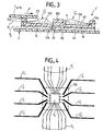
- FIG. 4 more particularly illustrates the wiring of the integrated circuit I C. This is shown in its cavity 105, seen from above with respect to FIG. 3.
- the brushes all end up in this cavity 105, on the left side, for the brushes C “ 1 to C” 4 , and on the right, for the brushes C " 5 to C” 8 , and they are connected to the I / O of the integrated circuit I C.
- two bundles of contact elements S i and S ' i , respectively, also connected to inputs-outputs of the integrated circuit I C.
- These contact elements play a role similar to the contact elements S 1 to S 11 of FIG. 2. They are connected, via the printed circuit 4, to the electronic circuits of the reader (not shown).
- FIG. 5a illustrates another embodiment of a 1 "connector according to the invention.
- the zone 105 ′ in which the integrated circuit is located (I C ) is offset laterally with respect to the pairs of contacts C 1 to C 8
- the contact pads to be connected to the inputs / outputs of the integrated circuit I C are located in a plane coincident with the plane P 2 , as defined above. They are connected, as described, either directly to the electronic circuits of the reader, or to the pair of limit switches C fc1 -C fc2 , or to the ground and to the corresponding brush C 5 , or again to the brush d power supply C 1 (and possibly to certain signal brushes in an exemplary embodiment not described).
- the bundle of direct links with the electronic circuits of the reader is identified under the general reference f Si .
- the ground link to the reader is labeled S ' 5 .
- the rear ends, 82 'to 84' and 86 'to 88', of the signal brushes (not connected to the inputs / outputs of the integrated circuit), C 2 to C 4 and C 6 to C 8 are raised and bent in the form of "S" flattened, so as to be flush in a plane P 3 situated at a higher level (in FIG. 5a) at the level of the plane P 2 . It is the same for the ends of the bundle of connections f Si which are flush with the plane P 3 , as well as the end of S ' 5 (ground connection).
- the ends of the supply brushes, C 1 , and of the ground brushes, C 5 are raised and curved but are substantially flush with the plane P 2 .
- This arrangement makes it possible to connect the appropriate pads of the circuit IC by means of conductive strips, CS 1 and CS 5 , respectively, to the brushes C 1 and C 5 . These blades are included in the plane P 2 .
- FIG. 5b illustrates, in partial section, in more detail, the arrangement of the brushes and blades CS 1 and CS 2 mentioned above in the body 10 "of the connector 1".
- the fragment illustrated shows the three brushes C1, C2 and C3 as well as the conductive strip CS 1 .
- the latter is arranged in a groove 106 ", orthogonal to the blades constituting the brushes. It can be seen that the ends 82 'and 83' are flush with the plane P 3 , while the end 81 'is just below the plane P 2 , so as to be connected with the CS 1 blade.
- the flexible blades forming the brushes are located substantially in the plane P 1 , over most of their length.
- the circuit I C provides the interface between at least part of the contact elements (brushes, "limit switch” contacts, etc.) usually used in connectors of Art Connu and l reader electronics.
- the management of the functions related to the control of the insertion, removal and correct positioning of the card C is “transparent” for this electronics. It suffices in particular to provide, via the contact elements S 1 to S 11 , the supply of electrical energy to the microcircuit of the card, which also serves to supply the integrated circuit I C.
- the main advantage is that the designer of a particular application, using a card reader, is relieved of the above management. He just has to select a connector, possibly of a particular model, offering such or such functionalities, in as an active component.
- the invention applies in many fields: cards bank or credit, phone card, "electronic wallet”, toll, staff pointing, access card (security), etc.
Landscapes
- Engineering & Computer Science (AREA)
- Physics & Mathematics (AREA)
- Theoretical Computer Science (AREA)
- Artificial Intelligence (AREA)
- Computer Vision & Pattern Recognition (AREA)
- General Physics & Mathematics (AREA)
- Architecture (AREA)
- Electromagnetism (AREA)
- Civil Engineering (AREA)
- Structural Engineering (AREA)
- Microelectronics & Electronic Packaging (AREA)
- Coupling Device And Connection With Printed Circuit (AREA)
- Credit Cards Or The Like (AREA)
- Details Of Connecting Devices For Male And Female Coupling (AREA)
- Adornments (AREA)
Claims (10)
- Verbindungsstück (1) für eine eine Mikroschaltung aufweisende Kartenleseeinheit (C), mit einem Gehäuse (2), das Bürstenkontaktelemente (C1 bis C8) trägt, die dazu bestimmt sind in elektrischen Kontakt mit den Leiterbereichen (3) zu gelangen, die mit der Mikroschaltung der Karte (C) verbunden sind, wenn diese Karte in das Verbindungsstück (1) eingeführt ist, wobei mindestens ein Teil der Bürstenkontaktelemente (C1 bis C8) an einer elektronischen Schaltung (Ic) angeschlossen ist, wobei die Schaltung Mittel umfaßt, um das Hineinführen oder das Entnehmen der in der Leseeinheit befindlichen Karte (C) zu überwachen, wobei diese Schaltung (Ic) andererseits an die elektronische Schaltung (4) des Kartenlesers angeschlossen ist, dadurch gekennzeichnet, daß das Verbindungsstück diese elektronische Schaltung (Ic) aufweist und trägt.
- Verbindungsstück nach Anspruch 1, dadurch gekennzeichnet, daß es zusätzliche Kontaktelemente (S1 bis S11) umfaßt, die dazu bestimmt sind an die elektronische Schaltung (4) der Leseeinheit angeschlossen zu werden, wobei die elektronische Schaltung (IC) vom Gehäuse des Verbindungsstücks getragen wird, das an mindestens einem Teil der zusätzlichen Kontaktelemente (S1 bis S11) angeschlossen ist.
- Verbindungsstück nach einem der Ansprüche 1 oder 2, dadurch gekennzeichnet, daß die elektronische Schaltung, ein IC-Chip und die Ein- und Ausgänge des Chips (IC) direkt an den Bürstenkontaktelementen (C1, C5) angeschlossen sind, und daß die Ein- und Ausgänge des Chips (IC) direkt an den zusätzlichen Kontaktelementen (S8 bis S11) an einem zweiten Ende angeschlossen sind.
- Verbindungsstück nach Anspruch 3, dadurch gekennzeichnet, daß ferner mindestens ein Teil der Bürstenkontaktelemente (C2 bis C4, C6 bis C8) direkt an mindestens einem Teil der zusätzlichen Kontaktelemente (S1 bis S7) an einem zweiten Ende angeschlossen sind, ohne über die Ein- und Ausgänge des Chips (IC) geleitet zu werden.
- Verbindungsstück nach einem der vorhergehenden Ansprüche, dadurch gekennzeichnet, daß es ferner Kontaktelemente zum Auffinden der "Endposition" (Cfc1-Cfc2) umfaßt, so daß das korrekte Einführen der Karte (Carte) in das Verbindungsstück (1) ermittelt wird.
- Verbindungsstück nach Anspruch 5, dadurch gekennzeichnet, daß die Kontaktelemente zum Auffinden der "Endposition" (Cfc1-Cfc2) an zusätzliche Kontaktelemente angeschlossen sind, die selber direkt an die Ein- und Ausgänge des Chips (IC) in der Weise angeschlossen sind, daß der Zustand dieser Kontaktelemente zum Auffinden der "Endposition" (Cfc1-Cfc2) durch die elektronische Schaltung (IC) überwacht wird.
- Verbindungsstück nach Anspruch 6, dadurch gekennzeichnet, daß die elektronische Schaltung (IC) die Energieversorgung von einem der zusätzlichen Kontaktelemente erhält, wobei eines dieser Bürstenkontaktelemente (C1) dazu bestimmt ist, die elektronische Energieversorgung an die Mikroschaltung weiterzuleiten, daß das Verbindungsstück eine integrierte Schaltfunktion umfaßt, und daß die effektive Versorgung des Elementes durch Betätigen der integrierten Schaltfunktion durchgeführt wird, wenn die elektronische Schaltung (IC) einen Zustand der Kontaktelemente zum Auffinden der "Endposition" (Cfc1-Cfc2) ermittelt, die angeben, daß die Karte (C) richtig eingeführt wurde, und diese Versorgung im umgekehrten Fall belegen, so daß das Anlegen und Zurücknehmen der Spannung an der Mikroschaltung der Karte (C) gesteuert wird.
- Verbindungsstück nach einem der Ansprüche 1 bis 7, dadurch gekennzeichnet, daß das Gehäuse (10) ein elektrisch isolierendes Material und zwei offene Ausbuchtungen (100, 101) aufweist, in denen die Bürstenkontaktelemente (C"1 bis C"8) und Ränder (102, 104) angeordnet sind, die für die Führung der Karte (C) bei ihrem Einführen einen Rahmen bilden.
- Verbindungsstück nach Anspruch 8, dadurch gekennzeichnet, daß jedes der Bürstenkontaktelemente (C"1 bis C"8) ein Blatt (23, 63) umfaßt, das in der die Ausbuchtungen (100, 101) überdeckenden Zone eine Feder bildet, so daß die Feder auf den durch die Mikroschaltung getragenen Leiterbereichen schleift, wenn die Karte (C) in das Verbindungsstück (1') eingeführt ist, wobei die Blätter zwischen den Rändern eingeschlossen sind und durch gebogene Teile (24, 64) verlängert werden, die in eine Ausbuchtung des Gehäuses münden, in der sich der IC-Chip (IC) befindet, und um an den Ein- und Ausgängen dieses Chips angeschlossen werden zu können.
- Kartenleseeinheit (C) mit Mikroschaltung, gekennzeichnet durch ein Verbindungsstück nach einem der vorhergehenden Ansprüche.
Applications Claiming Priority (3)
| Application Number | Priority Date | Filing Date | Title |
|---|---|---|---|
| FR9501271 | 1995-02-03 | ||
| FR9501271A FR2730328B1 (fr) | 1995-02-03 | 1995-02-03 | Connecteur pour appareil lecteur de carte a microcircuit et appareil lecteur de carte a microcircuit le comprenant |
| PCT/FR1996/000156 WO1996024111A1 (fr) | 1995-02-03 | 1996-01-30 | Connecteur pour appareil lecteur de carte a microcircuit et lecteur de carte comprenant un tel connecteur |
Publications (2)
| Publication Number | Publication Date |
|---|---|
| EP0807295A1 EP0807295A1 (de) | 1997-11-19 |
| EP0807295B1 true EP0807295B1 (de) | 1998-10-21 |
Family
ID=9475817
Family Applications (1)
| Application Number | Title | Priority Date | Filing Date |
|---|---|---|---|
| EP96902309A Expired - Lifetime EP0807295B1 (de) | 1995-02-03 | 1996-01-30 | Verbinder für mikroschaltungskartenlesegerät und kartenleser mit einem derartigen verbinder |
Country Status (13)
| Country | Link |
|---|---|
| US (1) | US6165021A (de) |
| EP (1) | EP0807295B1 (de) |
| JP (1) | JPH11500549A (de) |
| KR (1) | KR100420883B1 (de) |
| CN (1) | CN1173232A (de) |
| AT (1) | ATE172563T1 (de) |
| AU (1) | AU701547B2 (de) |
| CA (1) | CA2211344A1 (de) |
| DE (1) | DE69600834T2 (de) |
| ES (1) | ES2125096T3 (de) |
| FR (1) | FR2730328B1 (de) |
| RU (1) | RU2181908C2 (de) |
| WO (1) | WO1996024111A1 (de) |
Families Citing this family (20)
| Publication number | Priority date | Publication date | Assignee | Title |
|---|---|---|---|---|
| FR2743170B1 (fr) * | 1995-12-28 | 1998-02-06 | Framatome Connectors Int | Connecteur actif pour carte a puce |
| US5790659A (en) * | 1996-08-30 | 1998-08-04 | Telefonaktiebolaget Lm Ericsson | Subscriber identity module (SIM) card holder |
| FI991002L (fi) * | 1999-05-03 | 2000-11-04 | Nokia Mobile Phones Ltd | Toimikorttiliitin ja matkaviestin |
| DE19935188C2 (de) * | 1999-07-27 | 2002-06-13 | Amphenol Tuchel Elect | Kontaktblock für einen Chipkartenleser |
| US6942154B1 (en) * | 2000-02-24 | 2005-09-13 | Matsushita Electric Industrial Co, Ltd. | Card connector and portable telephone having the same |
| FR2805671B1 (fr) * | 2000-02-25 | 2002-07-26 | Sagem | Connecteur pour cartes a puce |
| US6769036B1 (en) * | 2000-05-16 | 2004-07-27 | Palm Source, Inc. | Method and system for enabling personal digital assistants and protecting stored private data |
| US6856595B1 (en) * | 2000-05-19 | 2005-02-15 | Mosaid Technologies, Inc. | Method and apparatus for providing input back pressure in an output buffered switch |
| US7344074B2 (en) * | 2002-04-08 | 2008-03-18 | Nokia Corporation | Mobile terminal featuring smart card interrupt |
| TW555110U (en) * | 2002-08-28 | 2003-09-21 | Carry Computer Eng Co Ltd | Adapter for xD memory card |
| CN100375100C (zh) * | 2002-09-25 | 2008-03-12 | Nxp股份有限公司 | 用于芯片卡的连接器 |
| WO2006057049A1 (ja) * | 2004-11-26 | 2006-06-01 | Kabushiki Kaisha Toshiba | カードおよびホスト機器 |
| EP1866830B1 (de) * | 2005-03-30 | 2008-12-24 | Nxp B.V. | Anschliessbares gehäuse für ein tragbares objekt |
| US7347731B1 (en) * | 2006-09-22 | 2008-03-25 | Motorola, Inc. | Submersible accessory connector |
| TWM308521U (en) * | 2006-09-26 | 2007-03-21 | Jess Link Products Co Ltd | Adapter card structure |
| US8061609B2 (en) * | 2007-05-14 | 2011-11-22 | Sony Ericsson Mobile Communications Ab | Space efficient card readers and electronic devices incorporating same |
| CN101242047B (zh) | 2008-02-26 | 2010-06-09 | 华为终端有限公司 | Usb连接件及usb装置 |
| ES2413164R1 (es) * | 2011-10-10 | 2013-10-10 | Televes Sa | Cofre para equipos electronicos con sistema de conexionado para placa de circuito impreso |
| CN106033850B (zh) | 2015-03-13 | 2019-01-04 | 小米科技有限责任公司 | 智能卡卡座及电子设备 |
| CN113723122B (zh) * | 2021-08-30 | 2024-09-13 | 百富计算机技术(深圳)有限公司 | 读卡电路、读卡器及读卡系统 |
Family Cites Families (10)
| Publication number | Priority date | Publication date | Assignee | Title |
|---|---|---|---|---|
| FR2554260B1 (fr) * | 1983-10-27 | 1987-10-30 | Flonic Sa | Appareil de lecture de cartes a memoire electronique |
| US4840568A (en) * | 1987-03-31 | 1989-06-20 | Adc Telecommunications, Inc. | Jack assembly |
| FR2623313B1 (fr) * | 1987-11-13 | 1991-10-04 | Cit Alcatel | Cadre de contact pour lecteur de carte a puce |
| FR2623314B1 (fr) * | 1987-11-13 | 1991-06-14 | Cit Alcatel | Cadre de contact pour lecteur de carte a puce, avec contact de fin de course |
| GB2214680B (en) * | 1988-01-19 | 1991-07-31 | Technophone Ltd | Card reader |
| JPH0255355U (de) * | 1988-10-11 | 1990-04-20 | ||
| FR2668627A1 (fr) * | 1990-10-25 | 1992-04-30 | Cit Alcatel | Cadre de contact pour lecteur de carte a puce. |
| US5161992A (en) * | 1992-01-17 | 1992-11-10 | Amp Incorporated | Electrical connector assembly for a card containing an integrated circuit chip |
| RU2025057C1 (ru) * | 1992-08-12 | 1994-12-15 | Научно-исследовательский институт "Вектор" | Радиоэлектронный модуль |
| ATE176536T1 (de) * | 1995-03-22 | 1999-02-15 | Framatome Connectors Int | Leserrahmen für ic-kartenleser |
-
1995
- 1995-02-03 FR FR9501271A patent/FR2730328B1/fr not_active Expired - Fee Related
-
1996
- 1996-01-30 CA CA002211344A patent/CA2211344A1/fr not_active Abandoned
- 1996-01-30 EP EP96902309A patent/EP0807295B1/de not_active Expired - Lifetime
- 1996-01-30 DE DE69600834T patent/DE69600834T2/de not_active Expired - Fee Related
- 1996-01-30 ES ES96902309T patent/ES2125096T3/es not_active Expired - Lifetime
- 1996-01-30 US US08/875,694 patent/US6165021A/en not_active Expired - Fee Related
- 1996-01-30 AU AU46672/96A patent/AU701547B2/en not_active Ceased
- 1996-01-30 WO PCT/FR1996/000156 patent/WO1996024111A1/fr not_active Ceased
- 1996-01-30 AT AT96902309T patent/ATE172563T1/de not_active IP Right Cessation
- 1996-01-30 RU RU97114852/09A patent/RU2181908C2/ru not_active IP Right Cessation
- 1996-01-30 CN CN96191765A patent/CN1173232A/zh active Pending
- 1996-01-30 JP JP8523312A patent/JPH11500549A/ja active Pending
- 1996-01-30 KR KR1019970705297A patent/KR100420883B1/ko not_active Expired - Fee Related
Also Published As
| Publication number | Publication date |
|---|---|
| FR2730328A1 (fr) | 1996-08-09 |
| JPH11500549A (ja) | 1999-01-12 |
| AU4667296A (en) | 1996-08-21 |
| EP0807295A1 (de) | 1997-11-19 |
| CN1173232A (zh) | 1998-02-11 |
| DE69600834T2 (de) | 1999-04-15 |
| FR2730328B1 (fr) | 1997-04-04 |
| RU2181908C2 (ru) | 2002-04-27 |
| DE69600834D1 (de) | 1998-11-26 |
| WO1996024111A1 (fr) | 1996-08-08 |
| US6165021A (en) | 2000-12-26 |
| AU701547B2 (en) | 1999-01-28 |
| KR100420883B1 (ko) | 2004-05-20 |
| ES2125096T3 (es) | 1999-02-16 |
| KR19980701900A (ko) | 1998-06-25 |
| ATE172563T1 (de) | 1998-11-15 |
| CA2211344A1 (fr) | 1996-08-08 |
Similar Documents
| Publication | Publication Date | Title |
|---|---|---|
| EP0807295B1 (de) | Verbinder für mikroschaltungskartenlesegerät und kartenleser mit einem derartigen verbinder | |
| EP0815528B1 (de) | Leserrahmen für ic-kartenleser | |
| EP0343030B1 (de) | Flexible gedruckte Schaltung, insbesondere für elektronische Mikroschaltungskarten und Karte mit dieser Schaltung | |
| EP0139593B1 (de) | Apparat zum Ablesen von Karten mit elektronischen Speichern | |
| EP0262036B1 (de) | Datenverarbeitungssystem mit mit mehreren elektronischen Modulen versehenen Speicherkarten | |
| EP0274288B1 (de) | Verbindungseinrichtung für Karten mit elektronischem Speicher und Abtast/Schreibe-Vorrichtung, die diese verwendet | |
| EP0323347B1 (de) | Lese-/Schreibeinrichtung für Speicherkarte mit einer Vorrichtung gegen Betrug | |
| EP0819283B1 (de) | Datensammelsystem für kartenlesegerät | |
| FR2554262A1 (fr) | Dispositif anti-fraude pour lecteur de cartes a memoire electronique | |
| FR2808608A1 (fr) | Carte a memoire electronique destinee a etre introduite dans un dispositif de traitement | |
| CA2212951C (fr) | Connecteur pour appareil lecteur de carte a microcircuit | |
| EP0338900A1 (de) | Vorrichtung zur elektrischen Kontaktgabe von auf zwei Elemente verteilten Leitern und insbesondere zwischen denen einer Speicherkarte und deren Leseeinrichtung | |
| FR2613142A1 (fr) | Connecteur d'un dispositif de raccordement pour connexion avec une carte a circuits integres | |
| EP0980561B1 (de) | Entfernbare karte mit einer steckverbindung als smartkartenleser für einen mikrocomputer | |
| EP0676716A1 (de) | Tragbarer Digitalinformationsträger | |
| EP1079324A1 (de) | Ein eine Anzahl Chipkarten enthaltendes elektronisches Gerät | |
| EP1659492B1 (de) | Autonome elektronische Vorrichtung, insbesondere ein ambulantes medizinisches Aufnahmegerät, mit einem reprogrammierbaren Mikrocontroller | |
| EP2790124B1 (de) | Gesicherte Steckverbindung | |
| FR2997570A1 (fr) | Connecteur de carte a memoire securise. | |
| EP1045338B1 (de) | Elektronische Speicherkarte mit Kartensicherheitselement | |
| FR2619941A1 (fr) | Systeme de controle de la liaison entre deux terminaux d'une installation de traitement de donnees | |
| FR2695751A1 (fr) | Support d'informations à mémoire modifiable, lecteur de support d'informations adapté à utiliser un tel support, et système constitué par une tel lecteur. | |
| FR2880713A1 (fr) | Procede de commutation de voies de communication pour des circuits de cartes a puces, cartes a puces et appareil lecteur correspondant au procede | |
| FR2693295A1 (fr) | Circuit d'horloge pour dispositif de jeu. | |
| EP0624750A1 (de) | Vorrichtung zur Verbindung und logischen Verknüpfung einer Vielzahl von Schaltelementenpaaren |
Legal Events
| Date | Code | Title | Description |
|---|---|---|---|
| PUAI | Public reference made under article 153(3) epc to a published international application that has entered the european phase |
Free format text: ORIGINAL CODE: 0009012 |
|
| 17P | Request for examination filed |
Effective date: 19970807 |
|
| AK | Designated contracting states |
Kind code of ref document: A1 Designated state(s): AT BE CH DE ES FR GB IT LI NL SE |
|
| GRAG | Despatch of communication of intention to grant |
Free format text: ORIGINAL CODE: EPIDOS AGRA |
|
| 17Q | First examination report despatched |
Effective date: 19980108 |
|
| GRAG | Despatch of communication of intention to grant |
Free format text: ORIGINAL CODE: EPIDOS AGRA |
|
| GRAH | Despatch of communication of intention to grant a patent |
Free format text: ORIGINAL CODE: EPIDOS IGRA |
|
| GRAH | Despatch of communication of intention to grant a patent |
Free format text: ORIGINAL CODE: EPIDOS IGRA |
|
| GRAA | (expected) grant |
Free format text: ORIGINAL CODE: 0009210 |
|
| AK | Designated contracting states |
Kind code of ref document: B1 Designated state(s): AT BE CH DE ES FR GB IT LI NL SE |
|
| PG25 | Lapsed in a contracting state [announced via postgrant information from national office to epo] |
Ref country code: AT Free format text: LAPSE BECAUSE OF FAILURE TO SUBMIT A TRANSLATION OF THE DESCRIPTION OR TO PAY THE FEE WITHIN THE PRESCRIBED TIME-LIMIT Effective date: 19981021 |
|
| REF | Corresponds to: |
Ref document number: 172563 Country of ref document: AT Date of ref document: 19981115 Kind code of ref document: T |
|
| REG | Reference to a national code |
Ref country code: CH Ref legal event code: NV Representative=s name: SCHMAUDER & PARTNER AG PATENTANWALTSBUERO Ref country code: CH Ref legal event code: EP |
|
| GBT | Gb: translation of ep patent filed (gb section 77(6)(a)/1977) |
Effective date: 19981022 |
|
| REF | Corresponds to: |
Ref document number: 69600834 Country of ref document: DE Date of ref document: 19981126 |
|
| ITF | It: translation for a ep patent filed | ||
| REG | Reference to a national code |
Ref country code: ES Ref legal event code: FG2A Ref document number: 2125096 Country of ref document: ES Kind code of ref document: T3 |
|
| PLBE | No opposition filed within time limit |
Free format text: ORIGINAL CODE: 0009261 |
|
| STAA | Information on the status of an ep patent application or granted ep patent |
Free format text: STATUS: NO OPPOSITION FILED WITHIN TIME LIMIT |
|
| 26N | No opposition filed | ||
| PGFP | Annual fee paid to national office [announced via postgrant information from national office to epo] |
Ref country code: CH Payment date: 20010122 Year of fee payment: 6 |
|
| PGFP | Annual fee paid to national office [announced via postgrant information from national office to epo] |
Ref country code: ES Payment date: 20011211 Year of fee payment: 7 |
|
| REG | Reference to a national code |
Ref country code: GB Ref legal event code: IF02 |
|
| PG25 | Lapsed in a contracting state [announced via postgrant information from national office to epo] |
Ref country code: LI Free format text: LAPSE BECAUSE OF NON-PAYMENT OF DUE FEES Effective date: 20020131 Ref country code: CH Free format text: LAPSE BECAUSE OF NON-PAYMENT OF DUE FEES Effective date: 20020131 |
|
| REG | Reference to a national code |
Ref country code: CH Ref legal event code: PL |
|
| PG25 | Lapsed in a contracting state [announced via postgrant information from national office to epo] |
Ref country code: ES Free format text: LAPSE BECAUSE OF NON-PAYMENT OF DUE FEES Effective date: 20030131 |
|
| PGFP | Annual fee paid to national office [announced via postgrant information from national office to epo] |
Ref country code: NL Payment date: 20030131 Year of fee payment: 8 |
|
| PG25 | Lapsed in a contracting state [announced via postgrant information from national office to epo] |
Ref country code: NL Free format text: LAPSE BECAUSE OF NON-PAYMENT OF DUE FEES Effective date: 20040801 |
|
| REG | Reference to a national code |
Ref country code: ES Ref legal event code: FD2A Effective date: 20030131 |
|
| NLV4 | Nl: lapsed or anulled due to non-payment of the annual fee |
Effective date: 20040801 |
|
| PGFP | Annual fee paid to national office [announced via postgrant information from national office to epo] |
Ref country code: BE Payment date: 20050119 Year of fee payment: 10 |
|
| PGFP | Annual fee paid to national office [announced via postgrant information from national office to epo] |
Ref country code: GB Payment date: 20051215 Year of fee payment: 11 |
|
| PGFP | Annual fee paid to national office [announced via postgrant information from national office to epo] |
Ref country code: SE Payment date: 20051222 Year of fee payment: 11 Ref country code: FR Payment date: 20051222 Year of fee payment: 11 |
|
| PG25 | Lapsed in a contracting state [announced via postgrant information from national office to epo] |
Ref country code: BE Free format text: LAPSE BECAUSE OF NON-PAYMENT OF DUE FEES Effective date: 20060131 |
|
| PGFP | Annual fee paid to national office [announced via postgrant information from national office to epo] |
Ref country code: IT Payment date: 20060131 Year of fee payment: 11 Ref country code: DE Payment date: 20060131 Year of fee payment: 11 |
|
| PG25 | Lapsed in a contracting state [announced via postgrant information from national office to epo] |
Ref country code: SE Free format text: LAPSE BECAUSE OF NON-PAYMENT OF DUE FEES Effective date: 20070131 |
|
| PG25 | Lapsed in a contracting state [announced via postgrant information from national office to epo] |
Ref country code: DE Free format text: LAPSE BECAUSE OF NON-PAYMENT OF DUE FEES Effective date: 20070801 |
|
| EUG | Se: european patent has lapsed | ||
| GBPC | Gb: european patent ceased through non-payment of renewal fee |
Effective date: 20070130 |
|
| REG | Reference to a national code |
Ref country code: FR Ref legal event code: ST Effective date: 20070930 |
|
| PG25 | Lapsed in a contracting state [announced via postgrant information from national office to epo] |
Ref country code: GB Free format text: LAPSE BECAUSE OF NON-PAYMENT OF DUE FEES Effective date: 20070130 |
|
| BERE | Be: lapsed |
Owner name: *FRAMATOME CONNECTORS INTERNATIONAL Effective date: 20060131 |
|
| PG25 | Lapsed in a contracting state [announced via postgrant information from national office to epo] |
Ref country code: FR Free format text: LAPSE BECAUSE OF NON-PAYMENT OF DUE FEES Effective date: 20070131 |
|
| PG25 | Lapsed in a contracting state [announced via postgrant information from national office to epo] |
Ref country code: IT Free format text: LAPSE BECAUSE OF NON-PAYMENT OF DUE FEES Effective date: 20070130 |