CN1173232A - Connector for a smart card reader apparatus and card reader comprising same - Google Patents
Connector for a smart card reader apparatus and card reader comprising same Download PDFInfo
- Publication number
- CN1173232A CN1173232A CN96191765A CN96191765A CN1173232A CN 1173232 A CN1173232 A CN 1173232A CN 96191765 A CN96191765 A CN 96191765A CN 96191765 A CN96191765 A CN 96191765A CN 1173232 A CN1173232 A CN 1173232A
- Authority
- CN
- China
- Prior art keywords
- connector
- card
- mentioned
- integrated circuit
- card reader
- Prior art date
- Legal status (The legal status is an assumption and is not a legal conclusion. Google has not performed a legal analysis and makes no representation as to the accuracy of the status listed.)
- Pending
Links
- 238000003780 insertion Methods 0.000 claims abstract description 4
- 230000037431 insertion Effects 0.000 claims abstract description 4
- 238000012360 testing method Methods 0.000 claims description 5
- 230000000903 blocking effect Effects 0.000 claims description 3
- 230000005611 electricity Effects 0.000 claims description 2
- 239000011810 insulating material Substances 0.000 claims description 2
- 238000000034 method Methods 0.000 description 8
- 230000008569 process Effects 0.000 description 6
- 238000001514 detection method Methods 0.000 description 4
- 230000008901 benefit Effects 0.000 description 3
- 238000005516 engineering process Methods 0.000 description 3
- 238000007726 management method Methods 0.000 description 3
- 238000005452 bending Methods 0.000 description 2
- 238000011161 development Methods 0.000 description 2
- 230000018109 developmental process Effects 0.000 description 2
- 238000005538 encapsulation Methods 0.000 description 2
- 239000000284 extract Substances 0.000 description 2
- 238000004519 manufacturing process Methods 0.000 description 2
- 239000002184 metal Substances 0.000 description 2
- 238000003860 storage Methods 0.000 description 2
- 230000005540 biological transmission Effects 0.000 description 1
- 230000015572 biosynthetic process Effects 0.000 description 1
- 238000010276 construction Methods 0.000 description 1
- 238000013500 data storage Methods 0.000 description 1
- 238000013461 design Methods 0.000 description 1
- 238000010586 diagram Methods 0.000 description 1
- 238000006073 displacement reaction Methods 0.000 description 1
- 230000009977 dual effect Effects 0.000 description 1
- 230000000694 effects Effects 0.000 description 1
- 238000009434 installation Methods 0.000 description 1
- 230000010354 integration Effects 0.000 description 1
- 239000000463 material Substances 0.000 description 1
- 230000007246 mechanism Effects 0.000 description 1
- 238000002493 microarray Methods 0.000 description 1
- 238000012986 modification Methods 0.000 description 1
- 230000004048 modification Effects 0.000 description 1
- 230000003287 optical effect Effects 0.000 description 1
- 238000012545 processing Methods 0.000 description 1
- 230000009467 reduction Effects 0.000 description 1
- 230000008672 reprogramming Effects 0.000 description 1
- 238000011160 research Methods 0.000 description 1
- 230000004044 response Effects 0.000 description 1
- 239000004065 semiconductor Substances 0.000 description 1
- 230000009897 systematic effect Effects 0.000 description 1
- 238000003466 welding Methods 0.000 description 1
- 238000004804 winding Methods 0.000 description 1
Images


Classifications
-
- G—PHYSICS
- G06—COMPUTING; CALCULATING OR COUNTING
- G06K—GRAPHICAL DATA READING; PRESENTATION OF DATA; RECORD CARRIERS; HANDLING RECORD CARRIERS
- G06K7/00—Methods or arrangements for sensing record carriers, e.g. for reading patterns
- G06K7/06—Methods or arrangements for sensing record carriers, e.g. for reading patterns by means which conduct current when a mark is sensed or absent, e.g. contact brush for a conductive mark
-
- H—ELECTRICITY
- H01—ELECTRIC ELEMENTS
- H01R—ELECTRICALLY-CONDUCTIVE CONNECTIONS; STRUCTURAL ASSOCIATIONS OF A PLURALITY OF MUTUALLY-INSULATED ELECTRICAL CONNECTING ELEMENTS; COUPLING DEVICES; CURRENT COLLECTORS
- H01R13/00—Details of coupling devices of the kinds covered by groups H01R12/70 or H01R24/00 - H01R33/00
- H01R13/02—Contact members
- H01R13/22—Contacts for co-operating by abutting
- H01R13/24—Contacts for co-operating by abutting resilient; resiliently-mounted
- H01R13/2442—Contacts for co-operating by abutting resilient; resiliently-mounted with a single cantilevered beam
-
- E—FIXED CONSTRUCTIONS
- E04—BUILDING
- E04B—GENERAL BUILDING CONSTRUCTIONS; WALLS, e.g. PARTITIONS; ROOFS; FLOORS; CEILINGS; INSULATION OR OTHER PROTECTION OF BUILDINGS
- E04B2/00—Walls, e.g. partitions, for buildings; Wall construction with regard to insulation; Connections specially adapted to walls
- E04B2/74—Removable non-load-bearing partitions; Partitions with a free upper edge
- E04B2/7407—Removable non-load-bearing partitions; Partitions with a free upper edge assembled using frames with infill panels or coverings only; made-up of panels and a support structure incorporating posts
- E04B2/7453—Removable non-load-bearing partitions; Partitions with a free upper edge assembled using frames with infill panels or coverings only; made-up of panels and a support structure incorporating posts with panels and support posts, extending from floor to ceiling
-
- G—PHYSICS
- G06—COMPUTING; CALCULATING OR COUNTING
- G06K—GRAPHICAL DATA READING; PRESENTATION OF DATA; RECORD CARRIERS; HANDLING RECORD CARRIERS
- G06K7/00—Methods or arrangements for sensing record carriers, e.g. for reading patterns
- G06K7/0013—Methods or arrangements for sensing record carriers, e.g. for reading patterns by galvanic contacts, e.g. card connectors for ISO-7816 compliant smart cards or memory cards, e.g. SD card readers
- G06K7/0021—Methods or arrangements for sensing record carriers, e.g. for reading patterns by galvanic contacts, e.g. card connectors for ISO-7816 compliant smart cards or memory cards, e.g. SD card readers for reading/sensing record carriers having surface contacts
-
- G—PHYSICS
- G06—COMPUTING; CALCULATING OR COUNTING
- G06K—GRAPHICAL DATA READING; PRESENTATION OF DATA; RECORD CARRIERS; HANDLING RECORD CARRIERS
- G06K7/00—Methods or arrangements for sensing record carriers, e.g. for reading patterns
- G06K7/0013—Methods or arrangements for sensing record carriers, e.g. for reading patterns by galvanic contacts, e.g. card connectors for ISO-7816 compliant smart cards or memory cards, e.g. SD card readers
- G06K7/0056—Methods or arrangements for sensing record carriers, e.g. for reading patterns by galvanic contacts, e.g. card connectors for ISO-7816 compliant smart cards or memory cards, e.g. SD card readers housing of the card connector
- G06K7/0069—Methods or arrangements for sensing record carriers, e.g. for reading patterns by galvanic contacts, e.g. card connectors for ISO-7816 compliant smart cards or memory cards, e.g. SD card readers housing of the card connector including means for detecting correct insertion of the card, e.g. end detection switches notifying that the card has been inserted completely and correctly
-
- H—ELECTRICITY
- H01—ELECTRIC ELEMENTS
- H01R—ELECTRICALLY-CONDUCTIVE CONNECTIONS; STRUCTURAL ASSOCIATIONS OF A PLURALITY OF MUTUALLY-INSULATED ELECTRICAL CONNECTING ELEMENTS; COUPLING DEVICES; CURRENT COLLECTORS
- H01R13/00—Details of coupling devices of the kinds covered by groups H01R12/70 or H01R24/00 - H01R33/00
- H01R13/66—Structural association with built-in electrical component
- H01R13/665—Structural association with built-in electrical component with built-in electronic circuit
-
- E—FIXED CONSTRUCTIONS
- E04—BUILDING
- E04B—GENERAL BUILDING CONSTRUCTIONS; WALLS, e.g. PARTITIONS; ROOFS; FLOORS; CEILINGS; INSULATION OR OTHER PROTECTION OF BUILDINGS
- E04B2/00—Walls, e.g. partitions, for buildings; Wall construction with regard to insulation; Connections specially adapted to walls
- E04B2/74—Removable non-load-bearing partitions; Partitions with a free upper edge
- E04B2002/7481—Locating rails with adjustable curvature
Landscapes
- Engineering & Computer Science (AREA)
- Physics & Mathematics (AREA)
- Theoretical Computer Science (AREA)
- Computer Vision & Pattern Recognition (AREA)
- Artificial Intelligence (AREA)
- General Physics & Mathematics (AREA)
- Architecture (AREA)
- Microelectronics & Electronic Packaging (AREA)
- Electromagnetism (AREA)
- Civil Engineering (AREA)
- Structural Engineering (AREA)
- Coupling Device And Connection With Printed Circuit (AREA)
- Credit Cards Or The Like (AREA)
- Details Of Connecting Devices For Male And Female Coupling (AREA)
- Adornments (AREA)
Abstract
A connector (1) for an apparatus for reading smart cards (C), comprising a body supporting brush contact elements (C1-C8) for contacting the conductive pads of a chip on a card (C) inserted into the connector (1). The connector (1) comprises an electronic circuit (Ic) connected to at least one pair of the brush contact elements (C1-C8) and connectable to the electronic circuit (4) of the card reader. The electronic circuit (Ic) on the connector comprises means for controlling the insertion of the card (C) into the card reader and its withdrawal therefrom.
Description
The present invention relates to a kind of connector of intelligent card reader.
The invention still further relates to intelligent card reader with this connector.
In the present invention, our said card has the card of monolithic or polylith integrated circuit block (being called chip) for all.For example, it can be a credit card, perhaps is called (CAM card) memory card.Usually, one has microprocessor or a microcontroller on the integrated circuit chip on the card, and it also comprises a storage unit, routine PROM.This card is used to insert a special data read-write equipment.For easy, will claim that below this device instrument is a card reader, it also can write data and finishes other function (providing electric energy, test or the like) certainly.In the storage element that data storage is mentioned in front, it is generally the recess shape.Therefore data are read from storer or opposite write store.
In either case, input-output mechanism being arranged all on the card, is the contact region that is positioned on major planar surface of card.Various standard codes the have been arranged position of contact region.It not only is used for the input-output data, also is used for carrying out various tests (existence of test card, or the like) to integrated circuit power supply with according to purposes.Card reader has a set of contact electrode, and after card correctly inserted the connector that for this reason is provided with, electrode contacted conductively with aforesaid contact region.
Exist many problems in this class is used, need to solve simultaneously, these problems are:
1 must could be to the power supply of the integrated circuit on the card after contact electrode is in the tram of contact region of card.As powering when the malposition, not only can not finish the function of regulation, also can damage circuit on the integrated circuit.
2 especially, and the electrode that is used for signal must reach correct position before the integrated circuit energising.
3 users may walk OK a karaoke club (being called " extracting ") in (information) processing procedure.Therefore card reader must be able in time reflect, cuts off the electricity supply before so that reach the danger position position of integrated circuit danger (just for) at electrode.
4 reasons are whatsoever slipped up accidentally or are attempted to deceive, and use wrong object, and for example the plate of a conduction or a false card also may produce mistake.
Under all these situations, must stop the work of instrument, the cut-out power supply is so that reduce danger and or the termination deceptive practices that circuit damages.
There have been many card-reading system attempts to solve all or part of the problems referred to above now.They can be divided three classes.
The first kind is an electronic detection system.
In this type systematic, we carry out electro-detection earlier before the integrated circuit power supply, for example, and the resistance between the potential electrode.If the position that measured value not in the set-point scope, just can be determined card not to or have foreign matter to insert instrument.
This system has many problems, wherein has:
-system must all be suitable for blocking all integrated circuit that are equipped with on the market, at least the purposes of determining (for example bank card) is suitable for.And for a simple and single testing process, the kind of integrated circuit is too many.
-this detection is carried out between disabled position and working position.Be readily understood that in " extracting " process, system must react very soon.The electronic circuit that is used for this purpose is complicated and expensive.
Second class is the device that is called " landing ".Provided an example of this system among the France FR-A-2 628 901.
For this system, be stuck in and withstand a link stopper before contacting with electrode.Ka surface (principal plane) moves to electrode perpendicular to electrode then.
Safety is guaranteed by mechanical system fully.And we can also realize dual fail-safe with " stroke end " contact, and when card was not in the tram, " stroke end " contact stopped power supply process.Power supply is to guarantee by the height of electrode or by electronics trigger pip of " snapping into the position " closing of contact.For example European patent EP 0,139 593 has been introduced an example of this system.
The main problem of this system is: the mechanical system of finishing this function is complicated and expensive.
The 3rd class is the system of contact electrode and the friction of " stroke end " contact.For example, introduced an example of this system among the French Patent (FRP) FR-A-2 623 314.
For this system, card has " stroke end " contact with the connector that inserts, and when card is in the tram, it will trigger to integrated circuit and power.
Physical construction is simple and cheap, but it has a problem at least, must add the management loop of a management above-mentioned " stroke end " in the circuit of card reader.
In addition, also having some is the common problems of several systems.
In the system that utilizes electronic detection system or " stroke end " contact, must add the function of control card position in the circuit in card reader, so must in each instrument development process, study.
In order to quicken (performance history) and reduction expense, the development person of card reader uses microprocessor usually.It has good dirigibility, when owing to a variety of causes, when the purpose of use changes, has needed only reprogramming.But known to us, when finishing said function, logical program is handled than logical circuit and is handled slowly.
The objective of the invention is to address the above problem, and get rid of the inconvenience of present system.
According to the present invention, the smart card reader connector has a body, contact electrode is installed above, they and the bonding pad connection of integrated circuit when card inserts connector, it is characterized by: it has an electronic circuit, it with at least one pair of is connected in the above-mentioned contact electrode, will be connected the device that the electronic circuit on the connector has control card to insert and take out with card reader circuit on the one hand on the other hand in card reader.
Another object of the present invention is card reader with this connector of design.
And the present invention is on connector, rather than on the card reader, an electronic circuit is set, the various operations that its control card inserts card reader or extracts out from card reader.
Like this, we have simplified the structure of card reader.Card reader can be installed different connectors, and each connector has the insertion process that an electronic loop is used to control the card with different integrated circuit.
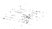
To understand the present invention better by following description, and embody the features and advantages of the present invention, relevant accompanying drawing is:
-Fig. 1 is a connector of the present invention, a skeleton view of the electronic circuit that the card of microarray strip and signal show, and connector will be connected with this electronic circuit,
-Fig. 2 is the synoptic diagram of taking apart of connector in the smart card reader,
-Fig. 3 is another example of the present invention, shows the longitudinal sectional view of connector in the smart card reader;
The position of-Fig. 4 used integrated circuit from the connector of top another example of demonstration the present invention.
-Fig. 5 a schematically shows the figure that takes apart of connector in the intelligent card reader, and this is an example of example of the present invention among Fig. 1;
-Fig. 5 b is the phantom view of this connector.
In the example of Fig. 1, the connector 1 with smart card reader C of integrated circuit 3 has a housing 2 supporting contact electrode part C 1 to C8.After card inserts connector 1, they will be connected with the contact region on the said integrated circuit C.
According to the present invention, this connector has a circuit I c, and it is connected to the part among the C8 with contact electrode C1 on the one hand at least, on the other hand, is connected with the circuit 4 of card reader.Circuit I c on the connector 1 has control card C to insert or extract out the device of connector, and this will be described in detail later.
Fig. 2 has schematically shown according to the present invention the structure of the connector 1 of an example.Or rather, we have only shown the relative position of the contact element of connector on this figure.
According to basic characteristics of the present invention, we are provided with an integrated circuit Ic in connector 1.Or rather, integrated circuit Ic is placed in the groove of connector Insulating frame (not shown) thickness direction.
Connector has two cover contact parts.
The first cover contact part is positioned at first plane P 1, or on the lower plane among Fig. 2, it comprises that a series of contact electrode is right; Be four pairs on the example in the drawings, C1 is to C8.These electrodes C1 is made up of the flexible sheets that is parallel to each other to C8, and bend its first termination 10 to 80, and head to head, after arrow C is inserted, the end will not contact with corresponding contact region (drawing) on the smart card at smart card.Preferably a pair of in addition " stroke end " contact in the first set of contact electrode correspondingly is Cfc1 and Cfc2.
In shown example, the acting as of electrode:
-contact part C 1: power supply;
-contact part C 5: ground wire;
-contact part C 2 is to C4 and C6 to C8: " signal " contact electrode (input and/or export).
In fact, this is identical with current structure.
Above-mentioned connector generally is connected in the printed circuit board (PCB) of card reader, for example will export and input adapter is welded on printed circuit board (PCB) and has in the hole of metal edges.Therefore, the conducting wire will have the hole of metal edges and the electronic circuit of card reader to couple together, so that the second set of contact part and electronic circuit are coupled together.
In the second set of contact part, can be divided into three classes according to their connection situation:
-the first kind: C '
2To C '
8(in this example) directly couple together by the contact electrode and the card reader electronic circuit of aforesaid printed wire connector 1.Usually, they are all or part signal contact electrodes (C1 to C4 and C6 to C8) in the example.With shown opposite of Fig. 2, the contact electrode C5 that connects ground wire also can be connected on the card reader in this way.
-the second class: C '
Fc1-C '
Fc2, C1 (in shown example) couples together the contact electrode of connector and some input/output terminals of integrated circuit.They are the contact parts that add, and are generally " stroke end " contact electrode C '
Fc1-C '
Fc2With power electrode C1.Sometimes, some signal contact electrode and ground line electrode C5 also can belong to this class.
-last, the 3rd class: S4, S8 be to S11, by aforementioned P.e.c. the output of integrated circuit Ic and/input end and card reader electronic circuit directly coupled together.One of above-mentioned union piece transmits integrated circuit Ic and passes the electric energy of coming.
In specific apparatus version shown in Figure 2, in order to simplify the manufacturing of connector, above a set of contact part C '
2To C '
4, C '
5To C '
8Respectively by the prolongation part S3 that is parallel to each other to S1, S4 prolongs to S7, the direction that prolongs part with contact part C '
2To C '
4, C '
6To C '
8Vertically.
Certainly, no matter whether ground wire contact electrode C5 directly connects, and integrated circuit Ic has one to be connected to ground wire (C ' among the figure just
5To S4) the ground wire link.
In order to show contact two set of contact parts more significantly, we will open two plane P 1 and P2 branch intentionally.In fact, two groups of parts are positioned at and lay respectively at plane P 1, on the P2, from very near, make contact electrode C1 to C8 and first end 10 to 80 opposite second end 11 to 81 with above a set of contact part C '
1To C '
8Corresponding end 12 to 82 connect.For corresponding " stroke end " contact part C
Fc1-C
Fc2And C '
Fc1-C '
Fc2Also be like this.
Corresponding contact part end can be with being welded to connect.
In order to connect the input and output side of integrated circuit Ic, can be by traditional welding technology.
The research of integrated circuit and manufacturing also are to use the advanced technology of common special IC.We have summarized monolithic integrated optical circuit and multichip integrated circuit with integrated circuit one speech.
The major function that integrated circuit Ic will finish is:
-detect " stroke end " to contact part C
Fc1-C
Fc2State;
-according to the aforesaid state control linkage or cut off to blocking the power supply of integrated circuit Carte; The function combinations of cutter is in integrated circuit Ic;
-detect the function of some electric property between the contact electrode: for example, resistance or impedance between two contact electrodes are perhaps to the response of a pulse signal;
-integrated some standard feature relevant with data transmission.
Present large-scale integration technology can integrated additional function, for example with developing intellectual resource card function associated.
All logic functions of card reader can also be set on connector 1 by integrated circuit Ic, and the electronic circuit beyond the connector only is the input and output loop.
Like this, the connector as driving part can be made different types, its difference can be finished different functions for integrated circuit.
Fig. 3 shows the cut-open view of connector 1 ' another example.This figure has shown the structure of connector body 10.
In Fig. 3, can only see a pair of contact electrode C "
2-C "
6, its function is identical to C2-C6 with respective electrode among Fig. 2.In fact, for same card, the contact electrode logarithm is the same." stroke end " contact electrode is equally also arranged to (not drawing among the figure).
Connector 1 ' body 10 is made for insulating material, and is the same with traditional structure, is supported on (not shown) on the printed-wiring board (PWB) of card reader.(by direction as shown) has two grooves 100 and 101, the both sides of the projection 103 that mediates respectively on the body up.We are provided with contact electrode in these grooves, for example, and the perhaps corresponding first half 23,63 of these electrodes more precisely.In this example, contact electrode is more longer, it self doubling, so that can put into definite zone of connector 1 ' body 10 fully, its other end stretches out from the inner groovy 105 that is placed with integrated circuit Ic.The advantage of this structure is can be directly the input-output end of integrated circuit Ic to be connected on the contact electrode, and need not be by middle contact part (as C ' among Fig. 21 or C ' 5).
We also can allow all contact electrodes be connected with integrated circuit, although according to function, only some contact electrode need be linked on the integrated circuit: power supply (electrode) or the like.Therefore only needing to prepare corresponding inside connects.
Fig. 4 shows the winding displacement situation of integrated circuit I c.It is arranged in groove 105, and view is to see from above with respect to Fig. 3.In this example, all electrodes all insert groove 105, electrode C "
1-C "
4On the left side, C "
5-C "
8On the right side, they all are connected on the input/output terminal of integrated circuit Ic.
We have also drawn two groups in the upper and lower of Fig. 4 and have contacted part Si and S ' i accordingly, and they also are connected on the input and output side of integrated circuit Ic.Among effect and Fig. 2 of these contact parts to contact part S1 identical to S11.They are connected by the circuit of P.e.c. 4 with card reader (not drawing).
In the superincumbent description, we suppose that semi-conductor chip Ic is a nude film, and the contact part has replaced the input-output pin.In other words, after the contact part is connected on the chip I c input/output terminal, must carry out special encapsulation, with the protection chip.We also can be installed in chip in the modular housing, this shell are installed in the groove 105 of connector 1 ' body 10 then.Can prevent attended operation and special encapsulation process like this.
Fig. 5 a shows connector 1 of the present invention " another example.
In this example, the zone 105 of integrated circuit (Ic) ' at contact electrode is installed to the next door of C1 to C8.To introduce as us, this layout makes can be only with an installation body.The contact region (plane at place) that is connected with integrated circuit Ic input/output terminal overlaps with the defined plane P 2 in front.With introduce previously the same, they otherwise directly be connected on the circuit of card reader, be connected the stroke end contact electrode on the Cfc1-Cfc2, be connected on ground wire and the corresponding contact electrode C5, or being connected power electrode C1 goes up (also might not be connected on some signal electrode) in having the example of introducing.The electrode that directly is connected on the card reader circuit generally is designated as fsi.The electrode that is connected to the card reader ground wire is designated as S ' 5.Signal electrode (electrode that is not connected with the input/output terminal of integrated circuit) C2 is also crooked to the rearward end perk of C8 to C2 and C6, the S of shape for flattening.It highly reaches plane 3, and (Fig. 5 a) is higher than plane 2.Equally, the end of connection electrode fsi and S ' 5 (ground wire link) also is on the plane P 3.On the contrary, power electrode C1 and ground line electrode C5 perk and bending, but highly only to plane P 2.This layout can be connected to corresponding electrode C1 and C5 by lead CS1 and CS2 with the corresponding bonding pad of integrated circuit Ic.These leads are arranged in plane P 2.
The mode that Fig. 5 b amplifies with partly cut-away shows the lead CS1 on the aforesaid connector 1 " body 10 " and the arrangement mode of CS2 and electrode in greater detail.Three electrode C1 have been shown, the part of C2 and C3 and lead CS1.The latter is positioned at the groove vertical with electrode 106 ".We can see end 82 ' and 83 ' be positioned at plane P 3, and end 81 ' below plane P 2, CS1 is connected with lead.
Thereby, we can (in plane P 3) directly weld all connection electrode fsi, connect the end of ground wire S ' 5 and all signal electrode, that is to say, all not with the direct-connected electrode of integrated circuit input-output terminal or integrated circuit Ic contact region.The signal that our hypothesis is sent Cfc1-Cfc2 by the stroke end contact electrode leads to integrated circuit to be handled.This end to electrode is positioned on the plane P 2, so that be connected with two connecting pins of integrated circuit Ic.
As before, most of length of the flexible sheets of formation electrode is arranged in plane P 1.
Above description explanation, integrated circuit Ic guarantees being connected between at least one pair of contact part (electrode, stroke end electrode etc.) and the card reader circuit, these contact parts in present card-reading machine connector also through commonly used.In other words, the insertion of card, the function of taking-up and location circuit hereto is " transparent ".Only needing provides electric energy by contact part S1 to the integrated circuit of S11 on card, and it is powered to integrated circuit Ic equally.When card correctly inserts, or more generally, when using method is executed correctly (except " extracting " or deceptive practices etc.), the circuit of card reader will send and/or receive one and use corresponding signal therewith.
In the advantage of Jie Shaoing, main one is: the developer of a specific use card reader needn't consider above-mentioned management (function) more in the above.He only needs to select the connector with required function, as a functional part.
Certainly, example that the present invention is not limited to introduce above and application, we can carry out various modifications to them, and do not exceed scope of the present invention.
Equally, the present invention can be applied to many fields, bank card or credit card, and phonecard, " stored value card ", and access card, individual's card, the card of entering (safety card), or the like.
Claims (10)
1. the connector (1) of smart card reader (C), it has a body, contact electrode (C1 is to C8) is installed above, they and the bonding pad connection of integrated circuit when card (C) inserts connector (1), it is characterized by: it has an electronic circuit (Ic), it with at least one pair of is connected in the above-mentioned contact electrode (C1 is to C8), will be connected the device that the electronic circuit on the connector (Ic) has control card (C) to insert and take out with card reader circuit (4) on the one hand on the other hand in card reader.
2. by the described connector of claim 1, it is characterized by: it has additional contact part (S1 is to S11), be used for being connected with card reader circuit (4), the electronic circuit on the connector body (Ic) at least with above-mentioned additional contact part (S1 is to S11) in a pair of the connection.
3. by described connector in claim 1 or 2, it is characterized by: above-mentioned electronic circuit is an integrated circuit (IC) chip, and the input/output terminal of this chip (Ic) is direct and above-mentioned connection electrode (C1, C5) connect, the input/output terminal of chip (Ic) directly is connected with above-mentioned additional contact part (S8 is to S11) by the second end.
4. by the described connector of claim 3, it is characterized by: in addition, have at least a pair of above-mentioned contact electrode (C2 is to C4, and C5 is to C8) directly to be connected on the second end of the above-mentioned additional contact part of at least a portion, and do not pass through the input/output terminal of chip (Ic).
5. any described connector in being required by aforesaid right is characterized by: whether the contact part (Cfc1-Cfc2) that it detects the stroke end in addition, correctly insert in the connector (1) in order to test card.
6. by the described connector of claim 5, it is characterized by: above-mentioned stroke end point determination contact part (Cfc1-Cfc2) is connected with additional contact part, and additional contact part directly is connected with the input-output end of said chip (Ic), and the state that makes the stroke end detect contact part (Cfc1-Cfc2) is subjected to electronic circuit (Ic) control.
7. by the described connector of claim 6, it is characterized by: one of above-mentioned contact electrode (C1) will be powered to said integrated circuit, and integrated circuit (Ic) obtains electric energy by additional contact part, and, connector has an integrated isolating switch, insert when above-mentioned stroke end point determination contact part (Cfc1-Cfc2) indicating card (C) is correct, above-mentioned integrated isolating switch will be controlled power supply, electric energy transmits by contact electrode (C1), under opposite situation, then cut off the electricity supply, make that the integrated circuit on the card (C) is switched on or outage.
8. by any described connector in the claim 1 to 7, it is characterized by: above-mentioned body (10) is to make with insulating material, and it has two grooves (100,101), above-mentioned contact electrode (C "
1To C "
8) being positioned at this two grooves, side (102 and 104) constitutes the guiding when blocking (C) insertion.
9. by the described connector of claim 8, it is characterized by: above-mentioned each contact electrode (C
1" to C
8") is a spring leaf (23; 63); cover groove (100; 101), and when card (C) inserts connector (1 '), they will slide on the conduction region of said integrated circuit; these sheets are sandwiched in the side; its extension is folded (24,64) other end and extends in the groove of laying integrated circuit (IC) chip (Ic) on the body, so that be connected with the input/output terminal of chip.
10. intelligent card reader, it is characterized by: it has the described connector of aforesaid right requirement.
Applications Claiming Priority (2)
| Application Number | Priority Date | Filing Date | Title |
|---|---|---|---|
| FR95/01271 | 1995-02-03 | ||
| FR9501271A FR2730328B1 (en) | 1995-02-03 | 1995-02-03 | CONNECTOR FOR MICROCIRCUIT CARD READING APPARATUS AND MICROCIRCUIT CARD READING APPARATUS INCLUDING SAME |
Publications (1)
| Publication Number | Publication Date |
|---|---|
| CN1173232A true CN1173232A (en) | 1998-02-11 |
Family
ID=9475817
Family Applications (1)
| Application Number | Title | Priority Date | Filing Date |
|---|---|---|---|
| CN96191765A Pending CN1173232A (en) | 1995-02-03 | 1996-01-30 | Connector for a smart card reader apparatus and card reader comprising same |
Country Status (13)
| Country | Link |
|---|---|
| US (1) | US6165021A (en) |
| EP (1) | EP0807295B1 (en) |
| JP (1) | JPH11500549A (en) |
| KR (1) | KR100420883B1 (en) |
| CN (1) | CN1173232A (en) |
| AT (1) | ATE172563T1 (en) |
| AU (1) | AU701547B2 (en) |
| CA (1) | CA2211344A1 (en) |
| DE (1) | DE69600834T2 (en) |
| ES (1) | ES2125096T3 (en) |
| FR (1) | FR2730328B1 (en) |
| RU (1) | RU2181908C2 (en) |
| WO (1) | WO1996024111A1 (en) |
Cited By (2)
| Publication number | Priority date | Publication date | Assignee | Title |
|---|---|---|---|---|
| CN100375100C (en) * | 2002-09-25 | 2008-03-12 | Nxp股份有限公司 | Connector for chip-card |
| CN113723122A (en) * | 2021-08-30 | 2021-11-30 | 百富计算机技术(深圳)有限公司 | Card reading circuit, card reader and card reading system |
Families Citing this family (16)
| Publication number | Priority date | Publication date | Assignee | Title |
|---|---|---|---|---|
| FR2743170B1 (en) * | 1995-12-28 | 1998-02-06 | Framatome Connectors Int | ACTIVE CONNECTOR FOR CHIP CARD |
| FI991002A (en) * | 1999-05-03 | 2000-11-04 | Nokia Mobile Phones Ltd | Active card adapter and telecommunicator |
| DE19935188C2 (en) * | 1999-07-27 | 2002-06-13 | Amphenol Tuchel Elect | Contact block for a chip card reader |
| US6942154B1 (en) * | 2000-02-24 | 2005-09-13 | Matsushita Electric Industrial Co, Ltd. | Card connector and portable telephone having the same |
| FR2805671B1 (en) * | 2000-02-25 | 2002-07-26 | Sagem | CONNECTOR FOR CHIP CARDS |
| US6769036B1 (en) * | 2000-05-16 | 2004-07-27 | Palm Source, Inc. | Method and system for enabling personal digital assistants and protecting stored private data |
| US6856595B1 (en) * | 2000-05-19 | 2005-02-15 | Mosaid Technologies, Inc. | Method and apparatus for providing input back pressure in an output buffered switch |
| US7344074B2 (en) * | 2002-04-08 | 2008-03-18 | Nokia Corporation | Mobile terminal featuring smart card interrupt |
| TW555110U (en) * | 2002-08-28 | 2003-09-21 | Carry Computer Eng Co Ltd | Adapter for xD memory card |
| WO2006057049A1 (en) * | 2004-11-26 | 2006-06-01 | Kabushiki Kaisha Toshiba | Card and host device |
| ATE418764T1 (en) * | 2005-03-30 | 2009-01-15 | Nxp Bv | CONNECTABLE HOUSING FOR A PORTABLE OBJECT |
| TWM308521U (en) * | 2006-09-26 | 2007-03-21 | Jess Link Products Co Ltd | Adapter card structure |
| US8061609B2 (en) * | 2007-05-14 | 2011-11-22 | Sony Ericsson Mobile Communications Ab | Space efficient card readers and electronic devices incorporating same |
| CN101242047B (en) * | 2008-02-26 | 2010-06-09 | 华为终端有限公司 | USB connection member and USB device |
| ES2413164R1 (en) * | 2011-10-10 | 2013-10-10 | Televes Sa | CHEST FOR ELECTRONIC EQUIPMENT WITH CONNECTION SYSTEM FOR PRINTED CIRCUIT PLATE |
| CN106033850B (en) * | 2015-03-13 | 2019-01-04 | 小米科技有限责任公司 | Smart card deck and electronic equipment |
Family Cites Families (7)
| Publication number | Priority date | Publication date | Assignee | Title |
|---|---|---|---|---|
| FR2554260B1 (en) * | 1983-10-27 | 1987-10-30 | Flonic Sa | ELECTRONIC MEMORY CARD READING APPARATUS |
| FR2623313B1 (en) * | 1987-11-13 | 1991-10-04 | Cit Alcatel | CONTACT FRAME FOR CHIP CARD READER |
| GB2214680B (en) * | 1988-01-19 | 1991-07-31 | Technophone Ltd | Card reader |
| JPH0255355U (en) * | 1988-10-11 | 1990-04-20 | ||
| FR2668627A1 (en) * | 1990-10-25 | 1992-04-30 | Cit Alcatel | CONTACT FRAME FOR CARD READER. |
| US5161992A (en) * | 1992-01-17 | 1992-11-10 | Amp Incorporated | Electrical connector assembly for a card containing an integrated circuit chip |
| DE69601497T2 (en) * | 1995-03-22 | 1999-06-17 | Framatome Connectors International, Courbevoie | READER FRAME FOR IC CARD READERS |
-
1995
- 1995-02-03 FR FR9501271A patent/FR2730328B1/en not_active Expired - Fee Related
-
1996
- 1996-01-30 DE DE69600834T patent/DE69600834T2/en not_active Expired - Fee Related
- 1996-01-30 CA CA002211344A patent/CA2211344A1/en not_active Abandoned
- 1996-01-30 KR KR1019970705297A patent/KR100420883B1/en not_active IP Right Cessation
- 1996-01-30 WO PCT/FR1996/000156 patent/WO1996024111A1/en active IP Right Grant
- 1996-01-30 RU RU97114852/09A patent/RU2181908C2/en not_active IP Right Cessation
- 1996-01-30 US US08/875,694 patent/US6165021A/en not_active Expired - Fee Related
- 1996-01-30 AT AT96902309T patent/ATE172563T1/en not_active IP Right Cessation
- 1996-01-30 ES ES96902309T patent/ES2125096T3/en not_active Expired - Lifetime
- 1996-01-30 CN CN96191765A patent/CN1173232A/en active Pending
- 1996-01-30 JP JP8523312A patent/JPH11500549A/en active Pending
- 1996-01-30 AU AU46672/96A patent/AU701547B2/en not_active Ceased
- 1996-01-30 EP EP96902309A patent/EP0807295B1/en not_active Expired - Lifetime
Cited By (2)
| Publication number | Priority date | Publication date | Assignee | Title |
|---|---|---|---|---|
| CN100375100C (en) * | 2002-09-25 | 2008-03-12 | Nxp股份有限公司 | Connector for chip-card |
| CN113723122A (en) * | 2021-08-30 | 2021-11-30 | 百富计算机技术(深圳)有限公司 | Card reading circuit, card reader and card reading system |
Also Published As
| Publication number | Publication date |
|---|---|
| KR100420883B1 (en) | 2004-05-20 |
| WO1996024111A1 (en) | 1996-08-08 |
| JPH11500549A (en) | 1999-01-12 |
| FR2730328A1 (en) | 1996-08-09 |
| AU701547B2 (en) | 1999-01-28 |
| RU2181908C2 (en) | 2002-04-27 |
| US6165021A (en) | 2000-12-26 |
| EP0807295A1 (en) | 1997-11-19 |
| CA2211344A1 (en) | 1996-08-08 |
| AU4667296A (en) | 1996-08-21 |
| FR2730328B1 (en) | 1997-04-04 |
| KR19980701900A (en) | 1998-06-25 |
| ES2125096T3 (en) | 1999-02-16 |
| ATE172563T1 (en) | 1998-11-15 |
| EP0807295B1 (en) | 1998-10-21 |
| DE69600834T2 (en) | 1999-04-15 |
| DE69600834D1 (en) | 1998-11-26 |
Similar Documents
| Publication | Publication Date | Title |
|---|---|---|
| CN1173232A (en) | Connector for a smart card reader apparatus and card reader comprising same | |
| CN1475957A (en) | Dual mode controller used on IS07816 and USB smart eard | |
| DE60219087T2 (en) | Terminal interface for smart cards | |
| US4675516A (en) | Apparatus for reading electronic memory cards | |
| US20130107472A1 (en) | Smartconnect flash card adapter | |
| US5564055A (en) | PCMCIA slot expander and method | |
| DE60124273T2 (en) | METHOD AND DEVICE FOR SIGNALING THE DATA TRANSFER BETWEEN A USB PORT AND A USB CHIP CARD MODULE | |
| US8265748B2 (en) | Defibrillator with a normalized electrode interface and defibrillating electrode | |
| KR100381938B1 (en) | Chip card module for biometric sensors | |
| EP0247368A1 (en) | Dual contact set for chip card reader | |
| CN1462014A (en) | Integral circuit device with multiple communication model and its operation method | |
| EP1486909A3 (en) | Smart card including a jtag test controller | |
| DE69411889T2 (en) | TRANSFER PROCEDURE WITH A PORTABLE CARRIER | |
| KR19980703279A (en) | Reader frame for smart card reader | |
| RU97114852A (en) | CONNECTOR FOR THE READING A CARD WITH A BUILT-IN CIRCUIT AND THE DEVICE FOR READING A CARD WITH SUCH A CONNECTOR | |
| US5929416A (en) | Reading head arrangement for two data card types | |
| CN2395401Y (en) | SIM card connector | |
| DE10255818A1 (en) | Miniature programmable control module for controlling an external load using a detachable output clamp carrier block | |
| DE10253286A1 (en) | fingerprint sensor | |
| CN211528970U (en) | Configuration data writing device for axle counting system | |
| CN1006829B (en) | Programmable logic controller system for hazardous environment | |
| US6419517B1 (en) | Apparatus and method for packaging circuits | |
| US20030080025A1 (en) | Configuration of a flat carrier with a chip module in a padded envelope and method of arranging the configuration | |
| JPH1049268A (en) | Method and device for extending pc card | |
| JPS6149290A (en) | Active memory card |
Legal Events
| Date | Code | Title | Description |
|---|---|---|---|
| C06 | Publication | ||
| PB01 | Publication | ||
| C10 | Entry into substantive examination | ||
| SE01 | Entry into force of request for substantive examination | ||
| C02 | Deemed withdrawal of patent application after publication (patent law 2001) | ||
| WD01 | Invention patent application deemed withdrawn after publication |