EP0806726A1 - Einrichtung und Verfahren zur On-line-Überwachung von Speichern - Google Patents
Einrichtung und Verfahren zur On-line-Überwachung von Speichern Download PDFInfo
- Publication number
- EP0806726A1 EP0806726A1 EP97106985A EP97106985A EP0806726A1 EP 0806726 A1 EP0806726 A1 EP 0806726A1 EP 97106985 A EP97106985 A EP 97106985A EP 97106985 A EP97106985 A EP 97106985A EP 0806726 A1 EP0806726 A1 EP 0806726A1
- Authority
- EP
- European Patent Office
- Prior art keywords
- memory
- error
- errors
- rate
- detection
- Prior art date
- Legal status (The legal status is an assumption and is not a legal conclusion. Google has not performed a legal analysis and makes no representation as to the accuracy of the status listed.)
- Granted
Links
Images


Classifications
-
- G—PHYSICS
- G06—COMPUTING OR CALCULATING; COUNTING
- G06F—ELECTRIC DIGITAL DATA PROCESSING
- G06F11/00—Error detection; Error correction; Monitoring
- G06F11/07—Responding to the occurrence of a fault, e.g. fault tolerance
- G06F11/08—Error detection or correction by redundancy in data representation, e.g. by using checking codes
- G06F11/10—Adding special bits or symbols to the coded information, e.g. parity check, casting out 9's or 11's
- G06F11/1008—Adding special bits or symbols to the coded information, e.g. parity check, casting out 9's or 11's in individual solid state devices
- G06F11/1048—Adding special bits or symbols to the coded information, e.g. parity check, casting out 9's or 11's in individual solid state devices using arrangements adapted for a specific error detection or correction feature
- G06F11/106—Correcting systematically all correctable errors, i.e. scrubbing
-
- G—PHYSICS
- G06—COMPUTING OR CALCULATING; COUNTING
- G06F—ELECTRIC DIGITAL DATA PROCESSING
- G06F11/00—Error detection; Error correction; Monitoring
- G06F11/07—Responding to the occurrence of a fault, e.g. fault tolerance
- G06F11/0703—Error or fault processing not based on redundancy, i.e. by taking additional measures to deal with the error or fault not making use of redundancy in operation, in hardware, or in data representation
- G06F11/0751—Error or fault detection not based on redundancy
- G06F11/0754—Error or fault detection not based on redundancy by exceeding limits
- G06F11/076—Error or fault detection not based on redundancy by exceeding limits by exceeding a count or rate limit, e.g. word- or bit count limit
-
- G—PHYSICS
- G06—COMPUTING OR CALCULATING; COUNTING
- G06F—ELECTRIC DIGITAL DATA PROCESSING
- G06F11/00—Error detection; Error correction; Monitoring
- G06F11/22—Detection or location of defective computer hardware by testing during standby operation or during idle time, e.g. start-up testing
- G06F11/2205—Detection or location of defective computer hardware by testing during standby operation or during idle time, e.g. start-up testing using arrangements specific to the hardware being tested
-
- G—PHYSICS
- G06—COMPUTING OR CALCULATING; COUNTING
- G06F—ELECTRIC DIGITAL DATA PROCESSING
- G06F11/00—Error detection; Error correction; Monitoring
- G06F11/30—Monitoring
- G06F11/34—Recording or statistical evaluation of computer activity, e.g. of down time, of input/output operation ; Recording or statistical evaluation of user activity, e.g. usability assessment
-
- G—PHYSICS
- G06—COMPUTING OR CALCULATING; COUNTING
- G06F—ELECTRIC DIGITAL DATA PROCESSING
- G06F2201/00—Indexing scheme relating to error detection, to error correction, and to monitoring
- G06F2201/81—Threshold
-
- G—PHYSICS
- G06—COMPUTING OR CALCULATING; COUNTING
- G06F—ELECTRIC DIGITAL DATA PROCESSING
- G06F2201/00—Indexing scheme relating to error detection, to error correction, and to monitoring
- G06F2201/865—Monitoring of software
Definitions
- the present invention relates the field of computer memory systems and the performance thereof.
- DRAM dynamic random access memory
- Such memories and systems incorporating such memories are known to be subject to certain types of errors. For instance, in the memory itself, the errors may be generally classified as either soft errors or hard errors. Soft errors are errors which occasionally occur, but are not repeatable, at least on a regular basis. Thus, soft errors alter data, though the stored data may be corrected by rewriting the correct data to the same memory location.
- a major cause of soft errors in DRAMs are alpha particles which, because of the very small size of DRAM storage cells, can dislocate sufficient numbers of electrons forming the charge determining the state of the cell to result in the cell being read as being in the opposite state.
- Soft errors can also be related to noise in the memory system, or due to unstable DRAMs or SIMMs (DRAMs in the form of single inline memory modules).
- Hard errors in the memory are repeatable errors which alter data due to some fault in the memory, and cannot be recovered by rewriting the correct data to the same memory location. Hard errors can occur when one memory cell becomes stuck in either state, or when SIMMs are not properly seated.
- Silent failures are failures that cannot be detected by the system. For example, if a standby part fails inside a system having redundant parts, most systems will remain unaware of the failure. However, although the system is still functional, it has lost its redundancy as if the same had never been provided, and is now vulnerable to a single failure of the operating part. Soft errors and hard errors can be either be single bit or multiple bit memory errors, and can also be silent failures under certain conditions.
- ECC error correction code
- server systems manufactured and sold by Sun Microsystems, Inc., assignee of the present invention are implemented with an error correction code (ECC) to protect the system from single bit memory errors.
- ECC error correction code
- the system automatically corrects the error before the data retrieved from memory is used.
- This is implemented using an 8-bit KANEDA error correction code for the 64-bit dataword of the memories, making the entire codeword 72-bits wide.
- the actual error detection and correction operation is done, for instance, by dedicated ECC circuitry as part of the processor module so that on the occurrence of a single bit memory error in the 72-bit codeword received from memory, the same will automatically be corrected before being presented to the processor.
- the processor upon the occurrence of a single bit error and the correction thereof by the ECC circuitry, the processor is alerted to that fact so that the processor will include the additional step of writing the corrected codeword (data and ECC) back to memory on the unverified assumption that the single bit error was a soft error.
- the I/O of the system consists of a 64-bit word, the applicable ECC code being tacked onto any dataword before the resulting 72-bit codeword is written to memory.
- an automatic reset is initiated upon the occurrence of a double bit memory error.
- This results in an interruption of service by the system, loss of any ongoing communication, and loss of data.
- a double bit error is a rare event under normal operating conditions, such system failures caused by double bit memory errors are also rare.
- normal operating conditions may be defined as operation without excessive memory errors occurring in the system, wherein the ECC implementation described provides adequate protection for the integrity of the system memory.
- two events can change a normal operating condition into an abnormal operating condition, specifically that (1) the memory subsystem has excessive single bit soft errors, and (2) the memory subsystem has single bit hard errors.
- a computer system incorporating the invention includes a memory and a processor, wherein the memory storage includes data storage and error correction code storage for each dataword.
- the system further includes automatic error detection and correction circuitry and software which monitors the occurrence of correction of errors and compares their frequency with the known frequency of soft errors for the memory devices being used to determine whether an alert is to be given and the nature of any such alert.
- the on-line memory monitoring system uses a unique statistical inference method developed to calculate the probability of the occurrence of multiple bit memory errors based on the number of single bit memory errors and the frequency of their occurrence as observed by the system. Once the probability is above a predetermined threshold, the on-line memory monitoring system will provide the appropriate alert.
- Figure 1 is a block diagram of the internal structure of the CPU/memory board of a system which may incorporate the present invention.
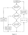
- Figure 2 is a logic flow diagram for the operation of the on-line memory monitoring system.
- Figure 3 illustrates a typical system that may use the present invention.
- FIG. 1 a block diagram of the internal structure of the CPU/memory board for the Enterprise X000 server systems to be introduced by Sun Microsystems, Inc., assignee of the present invention.
- the CPU/memory board contains two UltraSPARC modules containing high performance superscalar 64-bit SPARC processors. These modules are coupled through address and data controllers to memory and to a centerplane connector for connecting to a system bus structure. Also shown in Figure 1 is a boot controller and other on-board devices, their specific structure being well known and not important to the present invention.
- the memory is 72 bits wide, providing 64 bits of data and 8 bits of ECC.
- continuous on-line monitoring of memory errors is provided. As soon as the memory is found to have excessive single-bit soft errors relative to known statistics for such memories, or single-bit hard errors, a warning or alert may be presented to the system administrator so that corrective action can be taken.
- the on-line monitoring is done under software control, and continually monitors the system, logging all single-bit errors and the memory device in which such errors occurred. Upon the occurrence of another error, the on-line monitoring software analyzes the error log using statistical analysis to identify any abnormal operating condition that may be indicated.
- DRAMs dynamic random access memories
- An abnormal operating condition will be caused by either type of memory error, specifically excessive single-bit soft errors, or single-bit hard errors.
- both types of errors are single-bit errors that occur at an excessive rate.
- the hard errors can show up each time that part of the memory is accessed, while the soft errors may appear less frequently. This occurs because the hard errors are not correctable in memory by merely writing the corrected information back into memory.
- a bad memory cell hung in one state may or may not show up on any read access thereto as a hard error.
- a Poisson distribution is a single parameter and discrete event distribution.
- Table 2 shows the probability of having 0, 1, 2 and 3 or more failures per SIMM using 1 Mb DRAM.
- the on-line monitoring software can assess the system's operating condition based on the number of memory errors being detected. This can be accomplished by using a statistical analysis.
- a statistical inference method is developed to determine whether the system is running under normal operating conditions. This statistical inference method establishes two hypotheses as follows:
- the criteria for accepting H 0 or H 1 is based on the probability of the number of memory errors per SIMM that are observed during the test period. In the exemplary embodiment, if the probability is less than 0.0001 (0.01% chance of happening), an extremely unlikely event, the H 0 hypothesis is rejected and the alternative H 1 hypothesis is accepted. Rejecting H 0 means that the system, with very little doubt, is having excessive memory errors, and the system administrator should be alerted to take the necessary corrective steps. If the probability is higher than 0.0001, the event is considered to be a sufficiently likely event as to be within the statistics of normal operating conditions and the test continues. Obviously, the threshold between a sufficiently likely event to ignore and a sufficiently unlikely event to provide an alert may be altered as desired.
- the on-line monitoring is done by the processor under software control.
- the processor Upon the detection of a single-bit error detected and corrected by the ECC circuitry, the processor will carry out the further steps of updating the error log, apply the hypothesis test to the error log information, notify the system administrator of the type and location of the problem if appropriate, and write the corrected data and ECC information back into the memory location from which the data and ECC in error was obtained.
- the corrected data and ECC is written back into memory on the unverified assumption that the error was a soft error correctable by writing good data (and associated ECC) over the bad data and ECC.
- the following exemplary set of steps may be used (no particular order of the steps is to be implied herein and in the claims unless and only to the extent a particular step requires the completion of another step before the particular step may itself be completed).
- the on-line software in this exemplary embodiment will log the memory errors for up to three test periods (time periods) as listed in Table 3. Each time a memory error occurs, the software checks to see if the number of memory errors observed during the three test periods has exceeded the number of memory errors allowed for each of those time periods.
- the process will continue with no alert being given. If the number of allowable errors is exceeded for any of the time periods, the system administrator will be alerted by the processor. Based on the severity of the problem, preferably one of two levels of alarms are sent to the system administrator: a Red Flag indicating immediate action required, or a Yellow Flag indicating action required, but suggesting a less urgent requirement, as set out in Table 4 below:
- SIMM type memory components are being used, and since excessive single-bit memory errors can be caused by either a bad SIMM or an improperly seated SIMM, on an alert it may be preferable to first try to re-seat the SIMMs to see if the abnormal error condition repeats before replacing the SIMM.
- FIG. 2 a logic flow diagram for the operation of the preferred embodiment of the on-line memory monitoring system of the present invention may be seen.
- the first test is to check the error log to determine if the same SIMM has given a single bit error in the last two hours.
- the error is maintained as a running log, maintaining the log of the time the error occurred and the SIMM for which it occurred for all single bit errors for the longest test period used. For the 1 Mb and the 4 Mb devices of Table 3, the log would be maintained to cover the last 30 days. For the 16 Mb devices, the error log would be maintained to cover the last 22 days.
- the on-line memory monitoring system uses a unique statistical inference method previously described to calculate the probability of the occurrence of multiple bit memory errors based on the number of single bit memory errors and the frequency of their occurrence as observed by the system. Once the probability is above one or more predetermined probabilities, the on-line memory monitoring system will provide the appropriate alert.
- FIG. 3 A typical system that may use the present invention may be seen in Figure 3.
- an UltraSPARC processor CPU
- read/write random access memory and system controller are connected through a UPA Interconnect to the SBus to which various peripherals, communication connections and further bus connections are connected.
- the UPA (Ultra Port Architecture) Interconnect is a cache-coherent, processor-memory interconnect, the precise details of which are not important to the present invention.
- the error detection and correction circuitry is within the UPA Interconnect (though the ECC circuitry could be elsewhere in the data path to and from the memory, or for that matter the ECC function could be done in software, though this is not preferred because of speed considerations).
- the UPA Interconnect couples the CPU/memory in the system shown in Figure 3 to an Ethernet connection, and hard disk drives and a CDROM through a SCSI port. It also couples the CPU/memory to a serial port, a floppy disk drive and a parallel port, as well as a number of SBus connectors to which other SBus compatible devices may be connected.
- the software program for carrying out the operations of the flow chart of Figure 2 normally resides on one of the disk drives in the system.
- part of the code is loaded through the UPA Interconnect into the memory.
- This code causes the CPU to respond to the occurrence of a single bit error, as flagged and corrected by the ECC circuitry, by calling the rest of the on-line memory monitoring program code into memory and to execute the same to update the error log and to provide the appropriate warning flag to the system administrator.
Landscapes
- Engineering & Computer Science (AREA)
- Theoretical Computer Science (AREA)
- Quality & Reliability (AREA)
- Physics & Mathematics (AREA)
- General Engineering & Computer Science (AREA)
- General Physics & Mathematics (AREA)
- Techniques For Improving Reliability Of Storages (AREA)
- Debugging And Monitoring (AREA)
Applications Claiming Priority (2)
| Application Number | Priority Date | Filing Date | Title |
|---|---|---|---|
| US644314 | 1996-05-10 | ||
| US08/644,314 US5974576A (en) | 1996-05-10 | 1996-05-10 | On-line memory monitoring system and methods |
Publications (2)
| Publication Number | Publication Date |
|---|---|
| EP0806726A1 true EP0806726A1 (de) | 1997-11-12 |
| EP0806726B1 EP0806726B1 (de) | 2002-08-07 |
Family
ID=24584376
Family Applications (1)
| Application Number | Title | Priority Date | Filing Date |
|---|---|---|---|
| EP97106985A Expired - Lifetime EP0806726B1 (de) | 1996-05-10 | 1997-04-28 | Einrichtung und Verfahren zur On-line-Überwachung von Speichern |
Country Status (4)
| Country | Link |
|---|---|
| US (1) | US5974576A (de) |
| EP (1) | EP0806726B1 (de) |
| JP (1) | JPH1055320A (de) |
| DE (1) | DE69714507T2 (de) |
Cited By (11)
| Publication number | Priority date | Publication date | Assignee | Title |
|---|---|---|---|---|
| WO2004015717A3 (en) * | 2002-08-12 | 2006-06-01 | Intel Corp | Various methods and apparatuses to track failing memory locations to enable implementations for invalidating repeatedly failing memory locations |
| WO2009082557A1 (en) * | 2007-12-21 | 2009-07-02 | Sun Microsystems, Inc. | Prediction and prevention of uncorrectable memory errors |
| US8230255B2 (en) | 2009-12-15 | 2012-07-24 | International Business Machines Corporation | Blocking write acces to memory modules of a solid state drive |
| WO2013048467A1 (en) * | 2011-09-30 | 2013-04-04 | Intel Corporation | Generation of far memory access signals based on usage statistic tracking |
| US9317429B2 (en) | 2011-09-30 | 2016-04-19 | Intel Corporation | Apparatus and method for implementing a multi-level memory hierarchy over common memory channels |
| US9342453B2 (en) | 2011-09-30 | 2016-05-17 | Intel Corporation | Memory channel that supports near memory and far memory access |
| US9378133B2 (en) | 2011-09-30 | 2016-06-28 | Intel Corporation | Autonomous initialization of non-volatile random access memory in a computer system |
| US9378142B2 (en) | 2011-09-30 | 2016-06-28 | Intel Corporation | Apparatus and method for implementing a multi-level memory hierarchy having different operating modes |
| US9430372B2 (en) | 2011-09-30 | 2016-08-30 | Intel Corporation | Apparatus, method and system that stores bios in non-volatile random access memory |
| US9529708B2 (en) | 2011-09-30 | 2016-12-27 | Intel Corporation | Apparatus for configuring partitions within phase change memory of tablet computer with integrated memory controller emulating mass storage to storage driver based on request from software |
| US9600416B2 (en) | 2011-09-30 | 2017-03-21 | Intel Corporation | Apparatus and method for implementing a multi-level memory hierarchy |
Families Citing this family (30)
| Publication number | Priority date | Publication date | Assignee | Title |
|---|---|---|---|---|
| US6425108B1 (en) * | 1999-05-07 | 2002-07-23 | Qak Technology, Inc. | Replacement of bad data bit or bad error control bit |
| US6516429B1 (en) * | 1999-11-04 | 2003-02-04 | International Business Machines Corporation | Method and apparatus for run-time deconfiguration of a processor in a symmetrical multi-processing system |
| JP3474139B2 (ja) * | 2000-01-17 | 2003-12-08 | インターナショナル・ビジネス・マシーンズ・コーポレーション | コンピュータの電源制御方法、電源制御装置及びコンピュータ |
| US6701480B1 (en) * | 2000-03-08 | 2004-03-02 | Rockwell Automation Technologies, Inc. | System and method for providing error check and correction in memory systems |
| US6918078B2 (en) * | 2001-07-23 | 2005-07-12 | Intel Corporation | Systems with modules sharing terminations |
| US6985802B2 (en) * | 2003-04-22 | 2006-01-10 | Delphi Technologies, Inc. | Method of diagnosing an electronic control unit |
| US7480828B2 (en) | 2004-06-10 | 2009-01-20 | International Business Machines Corporation | Method, apparatus and program storage device for extending dispersion frame technique behavior using dynamic rule sets |
| JP4261462B2 (ja) * | 2004-11-05 | 2009-04-30 | 株式会社東芝 | 不揮発性メモリシステム |
| US20070011513A1 (en) * | 2005-06-13 | 2007-01-11 | Intel Corporation | Selective activation of error mitigation based on bit level error count |
| US7904760B2 (en) * | 2005-07-06 | 2011-03-08 | Cisco Technology, Inc. | Method and system for using presence information in error notification |
| JP5283845B2 (ja) * | 2007-02-07 | 2013-09-04 | 株式会社メガチップス | ビットエラーの予防方法、情報処理装置 |
| JP2008269473A (ja) * | 2007-04-24 | 2008-11-06 | Toshiba Corp | データ残存期間管理装置及び方法 |
| JP5082580B2 (ja) * | 2007-05-15 | 2012-11-28 | 富士通株式会社 | メモリシステム、メモリコントローラ、制御方法及び制御プログラム |
| US8140908B2 (en) * | 2007-06-22 | 2012-03-20 | Microsoft Corporation | System and method of client side analysis for identifying failing RAM after a user mode or kernel mode exception |
| US20090217281A1 (en) * | 2008-02-22 | 2009-08-27 | John M Borkenhagen | Adaptable Redundant Bit Steering for DRAM Memory Failures |
| US20100163756A1 (en) * | 2008-12-31 | 2010-07-01 | Custom Test Systems, Llc. | Single event upset (SEU) testing system and method |
| US8560927B1 (en) * | 2010-08-26 | 2013-10-15 | Altera Corporation | Memory error detection circuitry |
| CN102467417B (zh) * | 2010-11-19 | 2014-04-23 | 英业达股份有限公司 | 计算机系统 |
| US9749211B2 (en) | 2011-02-15 | 2017-08-29 | Entit Software Llc | Detecting network-application service failures |
| JP5691928B2 (ja) | 2011-08-05 | 2015-04-01 | 富士通株式会社 | プラグインカード収容装置 |
| US8819379B2 (en) | 2011-11-15 | 2014-08-26 | Memory Technologies Llc | Allocating memory based on performance ranking |
| US8707221B2 (en) * | 2011-12-29 | 2014-04-22 | Flextronics Ap, Llc | Circuit assembly yield prediction with respect to manufacturing process |
| JP5781003B2 (ja) * | 2012-04-26 | 2015-09-16 | 三菱電機株式会社 | 誤り検出訂正装置およびこれを備えた電子機器 |
| US9232630B1 (en) | 2012-05-18 | 2016-01-05 | Flextronics Ap, Llc | Method of making an inlay PCB with embedded coin |
| US9521754B1 (en) | 2013-08-19 | 2016-12-13 | Multek Technologies Limited | Embedded components in a substrate |
| US9565748B2 (en) | 2013-10-28 | 2017-02-07 | Flextronics Ap, Llc | Nano-copper solder for filling thermal vias |
| JP6866785B2 (ja) | 2017-06-29 | 2021-04-28 | 富士通株式会社 | プロセッサおよびメモリアクセス方法 |
| KR102413096B1 (ko) * | 2018-01-08 | 2022-06-27 | 삼성전자주식회사 | 전자 장치 및 그 제어 방법 |
| DE102020216072A1 (de) | 2020-12-16 | 2022-06-23 | Infineon Technologies Ag | Vorrichtung und Verfahren zum Bearbeiten von Bitfolgen |
| JP2026014617A (ja) * | 2024-07-19 | 2026-01-29 | 横河電機株式会社 | 制御装置、制御方法、および制御プログラム |
Citations (2)
| Publication number | Priority date | Publication date | Assignee | Title |
|---|---|---|---|---|
| US4809276A (en) * | 1987-02-27 | 1989-02-28 | Hutton/Prc Technology Partners 1 | Memory failure detection apparatus |
| US5263032A (en) * | 1991-06-27 | 1993-11-16 | Digital Equipment Corporation | Computer system operation with corrected read data function |
Family Cites Families (6)
| Publication number | Priority date | Publication date | Assignee | Title |
|---|---|---|---|---|
| US4319356A (en) * | 1979-12-19 | 1982-03-09 | Ncr Corporation | Self-correcting memory system |
| US4347600A (en) * | 1980-06-03 | 1982-08-31 | Rockwell International Corporation | Monitored muldem with self test of the monitor |
| US4531213A (en) * | 1982-03-03 | 1985-07-23 | Sperry Corporation | Memory through checking system with comparison of data word parity before and after ECC processing |
| US4792953A (en) * | 1986-03-28 | 1988-12-20 | Ampex Corporation | Digital signal error concealment |
| US5502732A (en) * | 1993-09-20 | 1996-03-26 | International Business Machines Corporation | Method for testing ECC logic |
| US5604753A (en) * | 1994-01-04 | 1997-02-18 | Intel Corporation | Method and apparatus for performing error correction on data from an external memory |
-
1996
- 1996-05-10 US US08/644,314 patent/US5974576A/en not_active Expired - Lifetime
-
1997
- 1997-04-28 DE DE69714507T patent/DE69714507T2/de not_active Expired - Fee Related
- 1997-04-28 EP EP97106985A patent/EP0806726B1/de not_active Expired - Lifetime
- 1997-05-12 JP JP9121038A patent/JPH1055320A/ja active Pending
Patent Citations (2)
| Publication number | Priority date | Publication date | Assignee | Title |
|---|---|---|---|---|
| US4809276A (en) * | 1987-02-27 | 1989-02-28 | Hutton/Prc Technology Partners 1 | Memory failure detection apparatus |
| US5263032A (en) * | 1991-06-27 | 1993-11-16 | Digital Equipment Corporation | Computer system operation with corrected read data function |
Non-Patent Citations (2)
| Title |
|---|
| "DOUBLE THRESHOLDING OF ERRORS", IBM TECHNICAL DISCLOSURE BULLETIN, vol. 32, no. 10B, 1 March 1990 (1990-03-01), pages 117, XP000097821 * |
| ANONYMOUS: "Error Frequency Warning Detector on Storage with ECC. November 1969.", IBM TECHNICAL DISCLOSURE BULLETIN, vol. 12, no. 6, November 1969 (1969-11-01), NEW YORK, US, pages 895, XP002037319 * |
Cited By (24)
| Publication number | Priority date | Publication date | Assignee | Title |
|---|---|---|---|---|
| WO2004015717A3 (en) * | 2002-08-12 | 2006-06-01 | Intel Corp | Various methods and apparatuses to track failing memory locations to enable implementations for invalidating repeatedly failing memory locations |
| WO2009082557A1 (en) * | 2007-12-21 | 2009-07-02 | Sun Microsystems, Inc. | Prediction and prevention of uncorrectable memory errors |
| US8468422B2 (en) | 2007-12-21 | 2013-06-18 | Oracle America, Inc. | Prediction and prevention of uncorrectable memory errors |
| US8495432B2 (en) | 2009-12-15 | 2013-07-23 | International Business Machines Corporation | Blocking write access to memory modules of a solid state drive |
| US8230255B2 (en) | 2009-12-15 | 2012-07-24 | International Business Machines Corporation | Blocking write acces to memory modules of a solid state drive |
| US9600416B2 (en) | 2011-09-30 | 2017-03-21 | Intel Corporation | Apparatus and method for implementing a multi-level memory hierarchy |
| US9619408B2 (en) | 2011-09-30 | 2017-04-11 | Intel Corporation | Memory channel that supports near memory and far memory access |
| US9342453B2 (en) | 2011-09-30 | 2016-05-17 | Intel Corporation | Memory channel that supports near memory and far memory access |
| US9378133B2 (en) | 2011-09-30 | 2016-06-28 | Intel Corporation | Autonomous initialization of non-volatile random access memory in a computer system |
| US9378142B2 (en) | 2011-09-30 | 2016-06-28 | Intel Corporation | Apparatus and method for implementing a multi-level memory hierarchy having different operating modes |
| US9430372B2 (en) | 2011-09-30 | 2016-08-30 | Intel Corporation | Apparatus, method and system that stores bios in non-volatile random access memory |
| US9529708B2 (en) | 2011-09-30 | 2016-12-27 | Intel Corporation | Apparatus for configuring partitions within phase change memory of tablet computer with integrated memory controller emulating mass storage to storage driver based on request from software |
| WO2013048467A1 (en) * | 2011-09-30 | 2013-04-04 | Intel Corporation | Generation of far memory access signals based on usage statistic tracking |
| US9600407B2 (en) | 2011-09-30 | 2017-03-21 | Intel Corporation | Generation of far memory access signals based on usage statistic tracking |
| US9317429B2 (en) | 2011-09-30 | 2016-04-19 | Intel Corporation | Apparatus and method for implementing a multi-level memory hierarchy over common memory channels |
| US10001953B2 (en) | 2011-09-30 | 2018-06-19 | Intel Corporation | System for configuring partitions within non-volatile random access memory (NVRAM) as a replacement for traditional mass storage |
| US10102126B2 (en) | 2011-09-30 | 2018-10-16 | Intel Corporation | Apparatus and method for implementing a multi-level memory hierarchy having different operating modes |
| US10241912B2 (en) | 2011-09-30 | 2019-03-26 | Intel Corporation | Apparatus and method for implementing a multi-level memory hierarchy |
| US10241943B2 (en) | 2011-09-30 | 2019-03-26 | Intel Corporation | Memory channel that supports near memory and far memory access |
| US10282322B2 (en) | 2011-09-30 | 2019-05-07 | Intel Corporation | Memory channel that supports near memory and far memory access |
| US10282323B2 (en) | 2011-09-30 | 2019-05-07 | Intel Corporation | Memory channel that supports near memory and far memory access |
| US10691626B2 (en) | 2011-09-30 | 2020-06-23 | Intel Corporation | Memory channel that supports near memory and far memory access |
| US10719443B2 (en) | 2011-09-30 | 2020-07-21 | Intel Corporation | Apparatus and method for implementing a multi-level memory hierarchy |
| US11132298B2 (en) | 2011-09-30 | 2021-09-28 | Intel Corporation | Apparatus and method for implementing a multi-level memory hierarchy having different operating modes |
Also Published As
| Publication number | Publication date |
|---|---|
| DE69714507T2 (de) | 2003-04-24 |
| US5974576A (en) | 1999-10-26 |
| JPH1055320A (ja) | 1998-02-24 |
| EP0806726B1 (de) | 2002-08-07 |
| DE69714507D1 (de) | 2002-09-12 |
Similar Documents
| Publication | Publication Date | Title |
|---|---|---|
| US5974576A (en) | On-line memory monitoring system and methods | |
| EP0075631B1 (de) | Gerät zur Registrierung von beständigen Speicherlesefehlern | |
| US4964130A (en) | System for determining status of errors in a memory subsystem | |
| US4661955A (en) | Extended error correction for package error correction codes | |
| EP0573307A2 (de) | Verfahren und Gerät zum Halten in und Rückgewinnen flüchtiger Daten aus einem Nachschreibcache im Falle eines Netzausfalls | |
| US20090150721A1 (en) | Utilizing A Potentially Unreliable Memory Module For Memory Mirroring In A Computing System | |
| US20030074598A1 (en) | Apparatus and method of repairing a processor array for a failure detected at runtime | |
| WO2017079454A1 (en) | Storage error type determination | |
| EP0281740B1 (de) | Speicher und deren Prüfung | |
| JPH04338849A (ja) | 記憶エラー訂正方法及び過剰エラー状態を報告する方法 | |
| JP2002278848A (ja) | アレイ・ビット線またはドライバの故障を予測報告するための、キャッシュしきい値処理の方法、装置、およびプログラム | |
| CN112732477A (zh) | 一种带外自检故障隔离的方法 | |
| CN113625957B (zh) | 一种硬盘故障的检测方法、装置及设备 | |
| US6842867B2 (en) | System and method for identifying memory modules having a failing or defective address | |
| EP1194849B1 (de) | System und verfahren zur verbesserung des multibit fehlerschutzes in einer computerspeichereinheit | |
| US7222271B2 (en) | Method for repairing hardware faults in memory chips | |
| US6035425A (en) | Testing a peripheral bus for data transfer integrity by detecting corruption of transferred data | |
| JP2001356968A (ja) | 故障許容データ格納システムおよび故障許容データ格納システムの動作方法 | |
| US5881072A (en) | Method of detecting error correction devices on plug-compatible memory modules | |
| CN112804234A (zh) | 一种应用于电力终端的嵌入式容侵容错装置及处理方法 | |
| US5644767A (en) | Method and apparatus for determining and maintaining drive status from codes written to disk drives of an arrayed storage subsystem | |
| US7389446B2 (en) | Method to reduce soft error rate in semiconductor memory | |
| CN100349125C (zh) | 一种对寄存器进行巡检校验的方法 | |
| JPH06175934A (ja) | 1ビットエラー処理方式 | |
| JPH05216771A (ja) | データ処理装置内の重要データの回復可能性を保証する方法と装置 |
Legal Events
| Date | Code | Title | Description |
|---|---|---|---|
| PUAI | Public reference made under article 153(3) epc to a published international application that has entered the european phase |
Free format text: ORIGINAL CODE: 0009012 |
|
| AK | Designated contracting states |
Kind code of ref document: A1 Designated state(s): DE FR GB IT NL SE |
|
| 17P | Request for examination filed |
Effective date: 19980508 |
|
| 17Q | First examination report despatched |
Effective date: 20000704 |
|
| GRAG | Despatch of communication of intention to grant |
Free format text: ORIGINAL CODE: EPIDOS AGRA |
|
| GRAG | Despatch of communication of intention to grant |
Free format text: ORIGINAL CODE: EPIDOS AGRA |
|
| GRAH | Despatch of communication of intention to grant a patent |
Free format text: ORIGINAL CODE: EPIDOS IGRA |
|
| RAP1 | Party data changed (applicant data changed or rights of an application transferred) |
Owner name: SUN MICROSYSTEMS, INC. |
|
| GRAH | Despatch of communication of intention to grant a patent |
Free format text: ORIGINAL CODE: EPIDOS IGRA |
|
| GRAA | (expected) grant |
Free format text: ORIGINAL CODE: 0009210 |
|
| AK | Designated contracting states |
Kind code of ref document: B1 Designated state(s): DE FR GB IT NL SE |
|
| REG | Reference to a national code |
Ref country code: GB Ref legal event code: FG4D |
|
| REF | Corresponds to: |
Ref document number: 69714507 Country of ref document: DE Date of ref document: 20020912 |
|
| ET | Fr: translation filed | ||
| PGFP | Annual fee paid to national office [announced via postgrant information from national office to epo] |
Ref country code: FR Payment date: 20030425 Year of fee payment: 7 |
|
| PG25 | Lapsed in a contracting state [announced via postgrant information from national office to epo] |
Ref country code: SE Free format text: LAPSE BECAUSE OF NON-PAYMENT OF DUE FEES Effective date: 20030429 |
|
| PLBE | No opposition filed within time limit |
Free format text: ORIGINAL CODE: 0009261 |
|
| STAA | Information on the status of an ep patent application or granted ep patent |
Free format text: STATUS: NO OPPOSITION FILED WITHIN TIME LIMIT |
|
| PGFP | Annual fee paid to national office [announced via postgrant information from national office to epo] |
Ref country code: DE Payment date: 20030618 Year of fee payment: 7 |
|
| 26N | No opposition filed |
Effective date: 20030508 |
|
| PGFP | Annual fee paid to national office [announced via postgrant information from national office to epo] |
Ref country code: NL Payment date: 20031031 Year of fee payment: 7 |
|
| EUG | Se: european patent has lapsed | ||
| PG25 | Lapsed in a contracting state [announced via postgrant information from national office to epo] |
Ref country code: NL Free format text: LAPSE BECAUSE OF NON-PAYMENT OF DUE FEES Effective date: 20041101 |
|
| PG25 | Lapsed in a contracting state [announced via postgrant information from national office to epo] |
Ref country code: DE Free format text: LAPSE BECAUSE OF NON-PAYMENT OF DUE FEES Effective date: 20041103 |
|
| PG25 | Lapsed in a contracting state [announced via postgrant information from national office to epo] |
Ref country code: FR Free format text: LAPSE BECAUSE OF NON-PAYMENT OF DUE FEES Effective date: 20041231 |
|
| NLV4 | Nl: lapsed or anulled due to non-payment of the annual fee |
Effective date: 20041101 |
|
| REG | Reference to a national code |
Ref country code: FR Ref legal event code: ST |
|
| PG25 | Lapsed in a contracting state [announced via postgrant information from national office to epo] |
Ref country code: IT Free format text: LAPSE BECAUSE OF NON-PAYMENT OF DUE FEES Effective date: 20050428 |
|
| PGFP | Annual fee paid to national office [announced via postgrant information from national office to epo] |
Ref country code: GB Payment date: 20160427 Year of fee payment: 20 |
|
| REG | Reference to a national code |
Ref country code: GB Ref legal event code: PE20 Expiry date: 20170427 |
|
| PG25 | Lapsed in a contracting state [announced via postgrant information from national office to epo] |
Ref country code: GB Free format text: LAPSE BECAUSE OF EXPIRATION OF PROTECTION Effective date: 20170427 |