EP0806007B1 - Module de commande parametrable comprenant un premier et un second compteur chargeable, circuit electronique comprenant une pluralite de tels modules de commande parametrables et procede de synthese d'un tel circuit - Google Patents
Module de commande parametrable comprenant un premier et un second compteur chargeable, circuit electronique comprenant une pluralite de tels modules de commande parametrables et procede de synthese d'un tel circuit Download PDFInfo
- Publication number
- EP0806007B1 EP0806007B1 EP96935276A EP96935276A EP0806007B1 EP 0806007 B1 EP0806007 B1 EP 0806007B1 EP 96935276 A EP96935276 A EP 96935276A EP 96935276 A EP96935276 A EP 96935276A EP 0806007 B1 EP0806007 B1 EP 0806007B1
- Authority
- EP
- European Patent Office
- Prior art keywords
- parameter
- control
- value
- control module
- input
- Prior art date
- Legal status (The legal status is an assumption and is not a legal conclusion. Google has not performed a legal analysis and makes no representation as to the accuracy of the status listed.)
- Expired - Lifetime
Links
Images


Classifications
-
- G—PHYSICS
- G06—COMPUTING OR CALCULATING; COUNTING
- G06F—ELECTRIC DIGITAL DATA PROCESSING
- G06F7/00—Methods or arrangements for processing data by operating upon the order or content of the data handled
- G06F7/60—Methods or arrangements for performing computations using a digital non-denominational number representation, i.e. number representation without radix; Computing devices using combinations of denominational and non-denominational quantity representations, e.g. using difunction pulse trains, STEELE computers, phase computers
- G06F7/62—Performing operations exclusively by counting total number of pulses ; Multiplication, division or derived operations using combined denominational and incremental processing by counters, i.e. without column shift
-
- G—PHYSICS
- G06—COMPUTING OR CALCULATING; COUNTING
- G06F—ELECTRIC DIGITAL DATA PROCESSING
- G06F30/00—Computer-aided design [CAD]
- G06F30/30—Circuit design
Definitions
- a parametrizable control module comprising first and second loadable counters, an electronic circuit comprising a plurality of such parametrized control modules, and a method for synthesizing such circuit.
- the invention relates to a parametrizable control module comprising a first and a second loadable counting means, the first counting means being connected to a primary clock input and having a first output feeding an enable input of the second counting means, and a second output of the second counting means feeding a module output.
- the generating of programmable bit trains has been disclosed in EP Patent Application 579 324.
- a parametrizable control module can be used as a flexible development element in a development system for large-scale electronic circuitry.
- a parametrizable control module is defined by the following tuple or set of integer values: PCM(p[],i[],p_param,p_param_bits,i_param,i_param_bits, where
- p values correspond to the Period of a repetitive bit sequence and i values correspond to the number of Iterations of the sequence.
- a parametrizable control module as defined in independent claim 1.
- Such a parametrizable control module has more flexibility incorporated through a serial structure thereof, without necessity for a microcontroller.
- At least one of such counting means has a parameter input, or a parameter select input, or a value select input.
- applicability of the parametrizable control module is raised greatly.
- the invention also relates to an electronic circuit comprising a plurality of parametrized control modules according to the above. In this manner, versatile controller apparatuses can be constituted in a straightforward manner.
- the invention also relates to a method for synthesizing a circuit as recited supra, through executing the steps of
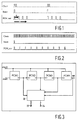
- Figure 1 shows the principle of an output bit sequence for given p and i.
- the first trace shows the clock signal that is recurrently generated by an external source. Generally, its period is uniform in time, although this is not a strict requirement.
- the second trace shows the reset signal, each reset causing in principle one full cycle of output pulses of the parametrizable control module or PCM. If the next reset signal occurs before the end of the preceding output cycle, the earlier cycle is generally aborted.
- the third trace shows the output signal train of the parametrizable control module. Therein, the period p has been indicated as the interval separating two neighbouring output pulses (as measured in clock periods), the multiplicity i as the total number of output pulses.
- a value that is hardwired into a control module is stored as (value minus one).
- parameters should be presented on an input port as (parameter minus one). Therefore, the example of Figure 2 is realized by storing a value of four with respect to p, and a value of nine with respect to i .
- FIG. 3 shows a module application configuration.
- the modules are configured to constitute a chain, the output of the preceding module feeding the reset of the next module, and all modules in parallel being controlled by the same clock.
- the circuit furthermore comprises a user module 20 that is controlled by the output signals of the respective modules.
- the user module receives user input signals on input 22 of arbitrary bit width and generates user output signals on output 24 of arbitrary bit width.
- a less extensive solution is to have only a single parametrizable control module.
- the construction of the user module generally falls outside the scope of the present invention.
- a bit sequence generator as defined in terms of a p vector and an i vector, which are used to hierarchically rebuild the bit sequence.
- a controller can be built using such modules.
- the p and i values will generally be unknown parameters.
- the parametrizable modules according to the invention may be used to implement the same functionality at a fraction of the costs. These modules may be chained into a pipeline by interposing a latch between each pair of modules, and resetting the first module in the chain one clock period earlier.
- Figure 4 shows a first module configuration 30 that has full facility. It comprises a p_down_counter 32 that receives a clock signal 40, a reset signal 42, a p_param(eter) value 50, a p_param(eter)_sel(ection) signal 52, and a p_select(ion) signal 54 of appropriate bit widths.
- the enable input 48 is always high at '1'.
- down counters are standard circuits under various different design systems and solid state technologies, and no further detailing on the transistor level is necessary. For an embodiment at gate level, see hereinafter. Carry output is normally zero, but upon attaining of the zero counter state becomes high.
- counter 34 receives the clock and reset signals.
- counter 34 receives the parameter value, parameter selection, and i selection signals.
- the enable signal for counter 34 is normally low, in that the output of AND gate 36 is low.
- the output of inverter 44 is normally high.
- the carry from counter 32, via OR 36 and AND 38, enables counter 34 for one clock pulse; also an output pulse is produced on output 56. At the next clock pulse, generally the carry from 32 is low again, thus disenabling counter 34.
- counter 34 attains zero, its carry becomes high, thereby blocking gate 36. The start of a new cycle necessitates a reset.
- the circuit as shown can be used for multiple hardwired p values and a p parameter (of which one is > 1), and also multiple hardwired i values and an i parameter (of which one is > 1).
- the word width of the p or i parameter is given by p_p and i_p, respectively.
- the values of p_p_s and i_p_s are 1.
- the number of bits necessary for selecting one hardwired p or i value are given by p_s and i_s, respectively.
- the control module of Figure 4 may be amended in several ways.
- a first amendment is to feed the enabling input 48 of down counter 32 by means of line 49 from inverter 44, instead of by means an external signal generator. In this way, less power is consumed. However, due to the long feedback line the circuit may operate less reliably at high clock frequencies.
- a second amendment is shown in Figure 5. Items 36, 38, 44, 46, 48, 56 have been shown in Figure 4. Two additional AND gates 39, 45 may be blocked by an external Enable signal EN. In this way, the operation of the circuit may be suspended during an arbitrarily long time. Again, due to the long feedback line the circuit may operate less reliably at high clock frequencies.
- Figure 6 shows a further module configuration 30 which is not subject of the present invention as claimed, that has restricted facilities.
- the second counter has been suppressed, together with input 54 of the upper counter.
- Gates 36, 38 may be suppressed as well.
- the layout can be maintained however. This configuration is used in case there is only a single one hardwired p value AND there is a p parameter input, one of which being > 1.
- Figure 7 shows a further second module configuration 30 which is not subject of the present invention as claimed that has restricted facilities.
- the first counter has been suppressed, together with input 62 of the lower counter.
- Gates 36, 38 may be suppressed as well.
- the layout can be maintained however. This configuration is used in case there is only a single one hardwired i value AND there is a i parameter input, one of which being > 1.
- the facilities can be even more restricted than in Figure 6, in that input 60 suppressed.
- the first counter can be suppressed, together with inputs 58, 60, whereas input 62 is maintained.
- the first counter can be suppressed, together with all three inputs 58, 60, 62.
- both the first and the second counters can be suppressed. In that case the module is rudimentary, in that only a connection from the reset input to output 56 need be realized.
- Figure 8 shows a down-counter configuration which is not subject of the present invention as claimed, that can be used for either of the preceding module realizations. This one is used when there are multiple preset start values (sl .. s3) and a parameter start value.
- the counter has clock input 90, reset input 86, and enable input 88.
- input 84 receives the p_selection signal. Now, the signal on input 82 selects one of the start values sl..s3; it should have an appropriate width for controlling multiplexer 94.
- the signal bit on input 84 selects between the start value presented, and the parameter signal fed from the input 80, by means of multiplexer 96.
- Multiplexer 106 feeds register 108 and is controlled by the reset and enable signals on inputs 86, 88, respectively, and by the carry signal from decrementer 110.
- the register output feeds decrementer 110 that has a data output (out) and a carry output; the latter produces a '1' when the register contains the value ..001.
- the carry is fed to output 92.
- Register 108 and decrementer 110 are activated by the clock signal.
- Multiplexer 106 receives the output signals from multiplexer 96, from register 108, and from decrementer 110. Multiplexer 106 is controlled by the reset and enable signals, in cooperation with the carry signal, by means of gates 98, 100, 102, 104.
- reset enable carry 98 100 102 104 value 0 0 0 0 0 0 0 0 0 0 0 0 1 0 0 0 0 0 0 1 0 1 0 1 0 1 2 1 0 0 0 0 1 0 0 2 1 0 1 0 0 1 0 2 1 1 1 0 1 0 1 0 1 2
- the counter configuration can be modified. First, if there is only a single preset start value, and a parameter start value, multiplexer 94 and the associated selection signal 84 may be suppressed. Second, if there is only a parameter start value, also multiplexer 96 and the associated control signal 84 may be suppressed, so that then input 80 directly feeds multiplexer 106. Third, if there are multiple preset start values, but no parameter start value, the output of multiplexer 94 may directly feed multiplexer 106, and inputs 80, 84, and multiplexer 96 may be suppressed. If there is only a single preset start value, multiplexers 94, 96, the associated control signals 82, 84, and parameter_in signal 80 may be suppressed, but the preset start value signal directly feeds multiplexer 106.
- Figures 9-11 illustrate an exemplary use of the control module according to the present invention.
- the application is the incremental generation of a data word sequence under the control of a chain of the invented modules.
- the data words may effectively represent addresses.
- the data word sequence is given as nested loops, as follows: The period wherein t increments is 18 clock ticks.
- the sequence of data words is: 0, 1, 2, 3, 4, 5, 6, 7, 8, 9, 10, 11, 16, 17, 18, 19, 20, 21, 22, 23, 24, 25, 26, 27, 32, 33, 34, 35, 36, 37, 38, 39, 40, 41, 42,....
- Figure 9 shows along the axis of time the instances on which the various data words are produced; these are not uniform in time.
- Figure 10 shows a first realization by means of three modules 120, 122, 124 according to the invention, wherein the production of '1' bits by the various modules has been shown along the time axis.
- the set-up has three multiplexers 128, 130, 132, controlled by the modules, a fourth multiplexer 136 controlled by the reset signal, register 126, and accumulator 134, and various signal generators as shown in blocks labelled with the increment values.
- the suspending of the progress can be executed again as shown in Figure 5.
- the module as described supra can be advantageously used in repetitive manner in a controller architecture described with reference to Figure 12.
- the control generation part 140 of such a design 146 contains all the parametrizable modules plus some further hardware, to produce all required control bit sequences.
- the condition generation block 142 contains the boolean logic necessary to convert the raw condition values into the set of more complex conditions which are required for the signals.
- the AND/OR network 144 implements the ANDing of bit sequences with conditions, together with the ORing of the results to produce the final control signals, as defined in the specification of the overall controller.
- control generation part 140 is the most complex block, of which the target architecture has been shown in Figure 13 by way of exemplary embodiment.
- input ports such as 150, 152, 170, 174, 176, latched in part, for receiving reset pulses generated elsewhere, and for parameters as specified.
- Shift registers such as 154, 164, 166, 168, that may be tapped, may be included to delay either the input pulses or the outputs of parametrizable control modules 156, 158, 160, 162, and the control modules may be interconnected to various output ports 178, 180, 182, 184, and reset ports as shown by way of example.
- clock input 172 is provided.
- each control signal is specified in terms of all conditions present, that are given in a list of conditions at the start of a specification, along with their possible values. Some of the conditions may be redundant, in that their value is don't care ⁇ *>. The latter conditions are removed from each signal specification.
- condition "latestripe" ⁇ 0,1>, “oddline” ⁇ 0,1>, “blockstart” ⁇ 0,1>, “blockend” ⁇ 0,1>, “firststripe” ⁇ 0,1>, “mem_hld” ⁇ 0,1>, “repeat” ⁇ 0,1>, “fieldno” ⁇ 0,1,2,3,>;
- Control signals that are defined in terms of control word sequences must be split into their constituent control bit sequences.
- the signal cyclic_0_ctrl was originally defined in terms of two-bit control words. Now, any signal with that name is split into two single-bit control signals named cyclic_0_ctrl_0 and cyclic_0_ctrl_1, respectively,whose only allowable difference may reside in the Required and Default values for the signals. Any signals with the same names after this stage must have the same Default values, but not by necessity the same Required values.
- any signals that have identical Required and Default values are thrown away, as they then need no longer a generator.
- Another optimization is as follows. Any signal defined in terms of more than one possible value of a condition is split up in as many equivalent signals as there are combinations of the conditions. Each of these signals will be exactly the same, apart from the single condition under which each is required.
- condition strings can then be used as input to a logic minimization software package describing the 'On-Set' for the channel, and are then translated back into conditions, with a single signal required for each condition string remaining.
- a reset signal is assigned to each signal in the specification, which takes the form of pulse_at_s, where s is either the actual start time for that signal, or the name of the parameter which describes that start time.
- a signal that now has empty period and iteration vectors represents a single pulse at the given start time.
- any signals that have period and iteration vectors with more than a single entry are split up into new signals that have single-entry vectors.
- Each such signal created is given a unique name temp_sig_UID, wherein UID is the identifier, and the reset signal for each control signal is made equal to the signal name just created. for example,
- the hardware implied by the specification is optimized before generating the netlist. While going to the specification so acquired, all different pairs p,I are picked up for control generating. Whilst iterating, for each p,I pair the control signals are searched that need such p,I values. These are separated into two groups. The first one contains those, whose control modules will be reset by an input pulse; the second, whose reset signal is produced by another module.
- the signals are sorted according to ascending start times, finding the minimum value of parameter start times if appropriate, and then begin;
Landscapes
- Engineering & Computer Science (AREA)
- Physics & Mathematics (AREA)
- Theoretical Computer Science (AREA)
- General Physics & Mathematics (AREA)
- Computer Hardware Design (AREA)
- General Engineering & Computer Science (AREA)
- Pure & Applied Mathematics (AREA)
- Mathematical Physics (AREA)
- Mathematical Optimization (AREA)
- Mathematical Analysis (AREA)
- Computing Systems (AREA)
- Computational Mathematics (AREA)
- Evolutionary Computation (AREA)
- Geometry (AREA)
- Logic Circuits (AREA)
- Pulse Circuits (AREA)
Claims (14)
- Module de commande paramétrable pour produire des séquences de bits de commande répétitives, comprenant un premier et un deuxième moyens de comptage chargeables (32, 34) pouvant être chargés de paramètres définissant lesdites séquences de bits de commande répétitives, le premier moyen de comptage (32) étant connecté à une entrée d'horloge primaire (40) et comportant une sortie alimentant une entrée de validation du deuxième moyen de comptage (34), et une sortie du deuxième moyen de comptage (34) alimentant la sortie de module (56) du module de commande paramétrable,
caractérisé en ce que lesdites sorties au moyen d'une porte de combinaison logique (36) alimentent toutes deux l'entrée de validation (46) du deuxième moyen de comptage (34) et la sortie de module (56), en ce que le deuxième moyen de comptage (34) est également cadencé par ladite entrée d'horloge primaire (40), et ledit module comportant une entrée de remise à zéro (42) qui alimente les entrées de remise à zéro des deux moyens de comptage et l'entrée de validation (46) du deuxième moyen de comptage (34). - Module de commande paramétrable suivant la revendication 1, au moins l'un des moyens de comptage comprenant une entrée de paramètres.
- Module de commande paramétrable suivant la revendication 2, au moins l'un des moyens de comptage comprenant une entrée de paramètres ainsi qu'une entrée de sélection de paramètres.
- Module de commande paramétrable suivant la revendication 1, 2 ou 3, au moins l'un des moyens de comptage comprenant une entrée de sélection de valeur.
- Module de commande paramétrable suivant l'une quelconque des revendications 1 à 4, dans lequel lesdits moyens de comptage comprennent un registre de valeurs de comptage qui est rétrocouplé au moyen d'un décrémenteur et d'un injecteur, ledit injecteur comprenant des moyens de commande pour, à la place d'une valeur rétrocouplée, injecter soit un paramètre, soit une valeur pour une décrémentation ultérieure.
- Module de commande paramétrable suivant la revendication 5, comprenant des moyens de sélection secondaires pour choisir entre ledit paramètre et ladite valeur.
- Module de commande paramétrable suivant la revendication 5 ou 6, comprenant des moyens de sélection ternaires pour choisir entre plusieurs exemples de ladite valeur.
- Circuit électronique comprenant une pluralité de modules de commande paramétrés suivant l'une quelconque des revendications 1 à 7.
- Circuit électronique suivant la revendication 8, dans lequel lesdits modules de commande paramétrés sont agencés en une chaíne en série.
- Système de contrôleur comprenant un ou plusieurs modules de commande paramétrables suivant l'une quelconque des revendications 1 à 7, étant contenu dans un bloc de production de commande, dans lequel des signaux conditionnels alimentent un bloc de production de conditions, et des sorties du bloc de production de conditions ainsi que des sorties du bloc de production de commande alimentent un réseau ET/OU pour de ce fait produire des signaux de commande pouvant être utilisés à l'extérieur,
et en ce que le comportement des signaux de commande éventuels produits peut être décrit de manière cyclique. - Système de contrôleur suivant la revendication 10, comprenant des modules de commande paramétrables de ce type suivant une organisation série et/ou parallèle.
- Procédé pour synthétiser un circuit électronique suivant la revendication 8 ou 9, ledit procédé comprenant les étapes suivantes :spécifier chaque signal de commande en termes d'une ou de plusieurs conditions réelles, avec des valeurs associées qui peuvent comprendre des valeurs de décalage ;dans chaque vecteur d'itération, trier toutes les valeurs apparaissant suivant une longueur de période dans un ordre monotone ;si un paramètre quelconque est présent, déterminer des valeurs minimale et maximale d'un tel paramètre pour tenir compte d'un tel tri jusqu'à ce que plus aucune différence univoque de taille ne dicte un nouveau tri suivant ledit ordre ;à la condition Si pn-1 = pn*In, alors : In-1 = In-1*In ; pn-1 = pn, ignorer pn et In et, si In-1 est un paramètre, attribuer In-1 à une autre valeur existante appropriée de paramètre, où une valeur Pi correspond à une période d'une séquence de bits répétitive et une valeur Ii correspond au nombre d'itérations de ladite séquence de bits répétitive ;ignorer toutes les paires p,I de vecteurs qui présentent p1 égal à la longueur de cycle et I1 = 1, etcartographier tous les paramètres vérifiés de cette façon sur la spécification de circuit pour une synthèse.
- Procédé suivant la revendication 12, dans lequel à la suite du dernier ignorer, pour les paires p,I restantes dont les modules de commande seront remis à zéro par une impulsion d'entrée, trier des signaux associés suivant les moments de début croissants, et résoudre de manière hiérarchique le problème de spécification de module de commande :en produisant un nom unique pour un module de commande avec des valeurs p et I uniques tel que donné control_module_p_I_UID ;pour chaque signal présentant le moment de début le plus bas, en définissant ce matériel égal à ce nom ;en définissant une variable this_sig_first_available sur ce moment de début, tout en, si le moment de début est un paramètre, trouvant sa valeur minimale à partir des définitions de paramètre, pour utiliser celle-ci comme moment de début ;en définissant la variable this_sig_now_desired sur le moment de début le plus élevé suivant ;si les deux moments trouvés aux deux dernières étapes sont sans rapport, en ce que leurs paramètres n'ont rien en commun ou qu'un moment est un paramètre et l'autre moment ne l'est pas, alors plutôt que d'utiliser un registre à décalage à longueur variable pour retarder le premier signal afin de produire le deuxième signal, en utilisant un nouveau module de commande pour produire plus tard le deuxième signal ;mais si les deux moments trouvés aux deux dernières étapes sont liés en ce que soit tous deux sont des valeurs réelles, soit tous deux sont définis par le même paramètre, alors en comparant le coût-surface d'un registre à décalage de longueur (this_sig_now_desired-this_sig_first_available) au coût-surface d'un module de commande supplémentaire pour les valeurs p,I données, et en sélectionnant la meilleure solution ;en définissant this_sig_first_available sur la valeur de this_sig_now_desired et en revenant à la dernière des deux étapes précédentes aussi longtemps qu'il existe d'autres signaux à implémenter.
- Procédé suivant la revendication 13, exécutant la même série d'étapes pour toutes les séquences de bits qui sont remises à zéro par une sortie d'un ou d'une série de modules de commande définis précédemment, jusqu'à ce que toutes les séquences de bits définies par des paires p,I comportent un nom d'un module de commande, tout en permettant une valeur de décalage/retard associée à celui-ci.
Priority Applications (1)
| Application Number | Priority Date | Filing Date | Title |
|---|---|---|---|
| EP96935276A EP0806007B1 (fr) | 1995-11-27 | 1996-11-18 | Module de commande parametrable comprenant un premier et un second compteur chargeable, circuit electronique comprenant une pluralite de tels modules de commande parametrables et procede de synthese d'un tel circuit |
Applications Claiming Priority (4)
| Application Number | Priority Date | Filing Date | Title |
|---|---|---|---|
| EP95203251 | 1995-11-27 | ||
| EP95203251 | 1995-11-27 | ||
| PCT/IB1996/001243 WO1997020268A1 (fr) | 1995-11-27 | 1996-11-18 | Module de commande parametrable comprenant un premier et un second compteur chargeable, circuit electronique comprenant une pluralite de tels modules de commande parametrables et procede de synthese d'un tel circuit |
| EP96935276A EP0806007B1 (fr) | 1995-11-27 | 1996-11-18 | Module de commande parametrable comprenant un premier et un second compteur chargeable, circuit electronique comprenant une pluralite de tels modules de commande parametrables et procede de synthese d'un tel circuit |
Publications (2)
| Publication Number | Publication Date |
|---|---|
| EP0806007A1 EP0806007A1 (fr) | 1997-11-12 |
| EP0806007B1 true EP0806007B1 (fr) | 2002-02-20 |
Family
ID=8220874
Family Applications (1)
| Application Number | Title | Priority Date | Filing Date |
|---|---|---|---|
| EP96935276A Expired - Lifetime EP0806007B1 (fr) | 1995-11-27 | 1996-11-18 | Module de commande parametrable comprenant un premier et un second compteur chargeable, circuit electronique comprenant une pluralite de tels modules de commande parametrables et procede de synthese d'un tel circuit |
Country Status (6)
| Country | Link |
|---|---|
| US (1) | US5828588A (fr) |
| EP (1) | EP0806007B1 (fr) |
| JP (1) | JP3830526B2 (fr) |
| KR (1) | KR100419549B1 (fr) |
| DE (1) | DE69619361T2 (fr) |
| WO (1) | WO1997020268A1 (fr) |
Families Citing this family (9)
| Publication number | Priority date | Publication date | Assignee | Title |
|---|---|---|---|---|
| US6216258B1 (en) | 1998-03-27 | 2001-04-10 | Xilinx, Inc. | FPGA modules parameterized by expressions |
| US6430732B1 (en) | 1998-03-27 | 2002-08-06 | Xilinx, Inc. | Method for structured layout in a hardware description language |
| US6292925B1 (en) * | 1998-03-27 | 2001-09-18 | Xilinx, Inc. | Context-sensitive self implementing modules |
| US6243851B1 (en) | 1998-03-27 | 2001-06-05 | Xilinx, Inc. | Heterogeneous method for determining module placement in FPGAs |
| US6237129B1 (en) | 1998-03-27 | 2001-05-22 | Xilinx, Inc. | Method for constraining circuit element positions in structured layouts |
| US6260182B1 (en) | 1998-03-27 | 2001-07-10 | Xilinx, Inc. | Method for specifying routing in a logic module by direct module communication |
| US20040127932A1 (en) * | 2002-09-12 | 2004-07-01 | Shah Tilak M. | Dip-molded polymeric medical devices with reverse thickness gradient, and method of making same |
| FR2905538B1 (fr) | 2006-08-30 | 2008-10-31 | Renault Sas | Generateur de signal logique pseudoperiodique. |
| WO2020141052A1 (fr) | 2018-12-31 | 2020-07-09 | Asml Netherlands B.V. | Imagerie améliorée par suppression d'ordre zéro |
Family Cites Families (7)
| Publication number | Priority date | Publication date | Assignee | Title |
|---|---|---|---|---|
| JPS63123218A (ja) * | 1986-11-12 | 1988-05-27 | Nec Corp | タイマ/カウンタ回路 |
| US5005193A (en) * | 1989-06-29 | 1991-04-02 | Texas Instruments Incorporated | Clock pulse generating circuits |
| FR2656124A1 (fr) * | 1989-12-15 | 1991-06-21 | Philips Laboratoires Electro | Multiplieur serie programmable. |
| FR2661297B1 (fr) * | 1990-04-18 | 1993-02-12 | Alcatel Radiotelephone | Circuit de multiplexage de signaux d'horloge. |
| US5261081A (en) * | 1990-07-26 | 1993-11-09 | Ncr Corporation | Sequence control apparatus for producing output signals in synchronous with a consistent delay from rising or falling edge of clock input signal |
| US5175753A (en) * | 1991-04-01 | 1992-12-29 | Advanced Micro Devices, Inc. | Counter cell including a latch circuit, control circuit and a pull-up circuit |
| DE69322818T2 (de) * | 1992-07-17 | 1999-07-29 | Koninkl Philips Electronics Nv | Mikroprozessor mit Taktzählung mit Hilfe von Registern, um bei einem zuvor bestimmten Zählerstand ein Befehlssignal einstellbarer Form zu erzeugen, und damit zu verwendendes hierarchisches Unterbrechungssystem |
-
1996
- 1996-11-18 WO PCT/IB1996/001243 patent/WO1997020268A1/fr not_active Ceased
- 1996-11-18 DE DE69619361T patent/DE69619361T2/de not_active Expired - Lifetime
- 1996-11-18 JP JP52031297A patent/JP3830526B2/ja not_active Expired - Lifetime
- 1996-11-18 KR KR1019970705060A patent/KR100419549B1/ko not_active Expired - Lifetime
- 1996-11-18 EP EP96935276A patent/EP0806007B1/fr not_active Expired - Lifetime
- 1996-11-25 US US08/755,673 patent/US5828588A/en not_active Expired - Lifetime
Also Published As
| Publication number | Publication date |
|---|---|
| DE69619361D1 (de) | 2002-03-28 |
| JPH11500848A (ja) | 1999-01-19 |
| WO1997020268A1 (fr) | 1997-06-05 |
| US5828588A (en) | 1998-10-27 |
| JP3830526B2 (ja) | 2006-10-04 |
| DE69619361T2 (de) | 2002-09-26 |
| EP0806007A1 (fr) | 1997-11-12 |
| KR100419549B1 (ko) | 2004-06-12 |
Similar Documents
| Publication | Publication Date | Title |
|---|---|---|
| US7047166B2 (en) | Method and VLSI circuits allowing to change dynamically the logical behavior | |
| US7577055B2 (en) | Error detection on programmable logic resources | |
| EP0806007B1 (fr) | Module de commande parametrable comprenant un premier et un second compteur chargeable, circuit electronique comprenant une pluralite de tels modules de commande parametrables et procede de synthese d'un tel circuit | |
| US6064232A (en) | Self-clocked logic circuit and methodology | |
| US5969553A (en) | Digital delay circuit and digital PLL circuit with first and second delay units | |
| US5029171A (en) | Test vector generation system | |
| US6504407B2 (en) | Programmable high speed frequency divider | |
| CN109669669A (zh) | 误码生成方法及误码生成器 | |
| US20060004980A1 (en) | Address creator and arithmetic circuit | |
| US4692640A (en) | Majority circuit comprising binary counter | |
| US12578386B2 (en) | Scan chain control | |
| CN1157507A (zh) | 数/模转换器接口装置 | |
| JPH07254853A (ja) | 同期式カウンタ | |
| US7123679B2 (en) | Counter having improved counting speed | |
| Vai et al. | Real-time maximum value determination on an easily testable VLSI architecture | |
| US6544806B1 (en) | Fast computation of truth tables | |
| RU2231921C2 (ru) | Троичное счетное устройство | |
| KR102508309B1 (ko) | 파이프 래치, 이를 이용하는 반도체 장치 및 반도체 시스템 | |
| JPH0722940A (ja) | 高速カウンタ | |
| SU830390A1 (ru) | Устройство дл обнаружени ошибокВ пАРАллЕльНОМ -РАзР дНОМ КОдЕС пОСТО ННыМ BECOM | |
| Sklyarov et al. | Reconfigurable Hierarchical Finite State Machines | |
| Aborhey | Binary decision based representation implementation of sequential systems | |
| Korobkova et al. | Synthesis of single series generators with rearrangeable pulse duration and its number in series | |
| Mehdipour et al. | A gravity-directed temporal partitioning approach | |
| Rhoad et al. | Digital Integrated Circuits: A Practical Application |
Legal Events
| Date | Code | Title | Description |
|---|---|---|---|
| PUAI | Public reference made under article 153(3) epc to a published international application that has entered the european phase |
Free format text: ORIGINAL CODE: 0009012 |
|
| AK | Designated contracting states |
Kind code of ref document: A1 Designated state(s): DE FR GB |
|
| 17P | Request for examination filed |
Effective date: 19971205 |
|
| GRAG | Despatch of communication of intention to grant |
Free format text: ORIGINAL CODE: EPIDOS AGRA |
|
| RIC1 | Information provided on ipc code assigned before grant |
Free format text: 7G 06F 7/62 A, 7G 06F 9/46 B |
|
| RIC1 | Information provided on ipc code assigned before grant |
Free format text: 7G 06F 7/62 A, 7G 06F 9/46 B |
|
| 17Q | First examination report despatched |
Effective date: 20010423 |
|
| GRAG | Despatch of communication of intention to grant |
Free format text: ORIGINAL CODE: EPIDOS AGRA |
|
| GRAH | Despatch of communication of intention to grant a patent |
Free format text: ORIGINAL CODE: EPIDOS IGRA |
|
| GRAH | Despatch of communication of intention to grant a patent |
Free format text: ORIGINAL CODE: EPIDOS IGRA |
|
| REG | Reference to a national code |
Ref country code: GB Ref legal event code: IF02 |
|
| GRAA | (expected) grant |
Free format text: ORIGINAL CODE: 0009210 |
|
| AK | Designated contracting states |
Kind code of ref document: B1 Designated state(s): DE FR GB |
|
| REF | Corresponds to: |
Ref document number: 69619361 Country of ref document: DE Date of ref document: 20020328 |
|
| ET | Fr: translation filed | ||
| REG | Reference to a national code |
Ref country code: GB Ref legal event code: 746 Effective date: 20020917 |
|
| REG | Reference to a national code |
Ref country code: FR Ref legal event code: D6 |
|
| PLBE | No opposition filed within time limit |
Free format text: ORIGINAL CODE: 0009261 |
|
| STAA | Information on the status of an ep patent application or granted ep patent |
Free format text: STATUS: NO OPPOSITION FILED WITHIN TIME LIMIT |
|
| 26N | No opposition filed |
Effective date: 20021121 |
|
| REG | Reference to a national code |
Ref country code: GB Ref legal event code: 732E |
|
| REG | Reference to a national code |
Ref country code: FR Ref legal event code: TP |
|
| REG | Reference to a national code |
Ref country code: FR Ref legal event code: ST Effective date: 20090731 |
|
| PGFP | Annual fee paid to national office [announced via postgrant information from national office to epo] |
Ref country code: DE Payment date: 20091112 Year of fee payment: 14 |
|
| PGFP | Annual fee paid to national office [announced via postgrant information from national office to epo] |
Ref country code: GB Payment date: 20091118 Year of fee payment: 14 Ref country code: FR Payment date: 20091123 Year of fee payment: 14 |
|
| REG | Reference to a national code |
Ref country code: FR Ref legal event code: D3 |
|
| GBPC | Gb: european patent ceased through non-payment of renewal fee |
Effective date: 20101118 |
|
| REG | Reference to a national code |
Ref country code: FR Ref legal event code: ST Effective date: 20110801 |
|
| REG | Reference to a national code |
Ref country code: DE Ref legal event code: R119 Ref document number: 69619361 Country of ref document: DE Effective date: 20110601 Ref country code: DE Ref legal event code: R119 Ref document number: 69619361 Country of ref document: DE Effective date: 20110531 |
|
| PG25 | Lapsed in a contracting state [announced via postgrant information from national office to epo] |
Ref country code: DE Free format text: LAPSE BECAUSE OF NON-PAYMENT OF DUE FEES Effective date: 20110531 |
|
| PG25 | Lapsed in a contracting state [announced via postgrant information from national office to epo] |
Ref country code: FR Free format text: LAPSE BECAUSE OF NON-PAYMENT OF DUE FEES Effective date: 20101130 |
|
| PG25 | Lapsed in a contracting state [announced via postgrant information from national office to epo] |
Ref country code: GB Free format text: LAPSE BECAUSE OF NON-PAYMENT OF DUE FEES Effective date: 20101118 |