EP0806005B1 - Procede et agencement permettant de faire fonctionner un dispositif informatique peripherique de stockage d'une memoire de grande capacite connecte a un ordinateur central - Google Patents
Procede et agencement permettant de faire fonctionner un dispositif informatique peripherique de stockage d'une memoire de grande capacite connecte a un ordinateur central Download PDFInfo
- Publication number
- EP0806005B1 EP0806005B1 EP96937864A EP96937864A EP0806005B1 EP 0806005 B1 EP0806005 B1 EP 0806005B1 EP 96937864 A EP96937864 A EP 96937864A EP 96937864 A EP96937864 A EP 96937864A EP 0806005 B1 EP0806005 B1 EP 0806005B1
- Authority
- EP
- European Patent Office
- Prior art keywords
- memory storage
- disk drive
- mass memory
- device driver
- loadable
- Prior art date
- Legal status (The legal status is an assumption and is not a legal conclusion. Google has not performed a legal analysis and makes no representation as to the accuracy of the status listed.)
- Expired - Lifetime
Links
Images
Classifications
-
- G—PHYSICS
- G06—COMPUTING OR CALCULATING; COUNTING
- G06F—ELECTRIC DIGITAL DATA PROCESSING
- G06F11/00—Error detection; Error correction; Monitoring
- G06F11/07—Responding to the occurrence of a fault, e.g. fault tolerance
- G06F11/0703—Error or fault processing not based on redundancy, i.e. by taking additional measures to deal with the error or fault not making use of redundancy in operation, in hardware, or in data representation
- G06F11/0706—Error or fault processing not based on redundancy, i.e. by taking additional measures to deal with the error or fault not making use of redundancy in operation, in hardware, or in data representation the processing taking place on a specific hardware platform or in a specific software environment
- G06F11/0727—Error or fault processing not based on redundancy, i.e. by taking additional measures to deal with the error or fault not making use of redundancy in operation, in hardware, or in data representation the processing taking place on a specific hardware platform or in a specific software environment in a storage system, e.g. in a DASD or network based storage system
-
- G—PHYSICS
- G06—COMPUTING OR CALCULATING; COUNTING
- G06F—ELECTRIC DIGITAL DATA PROCESSING
- G06F11/00—Error detection; Error correction; Monitoring
- G06F11/07—Responding to the occurrence of a fault, e.g. fault tolerance
- G06F11/0703—Error or fault processing not based on redundancy, i.e. by taking additional measures to deal with the error or fault not making use of redundancy in operation, in hardware, or in data representation
- G06F11/0766—Error or fault reporting or storing
-
- G—PHYSICS
- G06—COMPUTING OR CALCULATING; COUNTING
- G06F—ELECTRIC DIGITAL DATA PROCESSING
- G06F3/00—Input arrangements for transferring data to be processed into a form capable of being handled by the computer; Output arrangements for transferring data from processing unit to output unit, e.g. interface arrangements
- G06F3/06—Digital input from, or digital output to, record carriers, e.g. RAID, emulated record carriers or networked record carriers
- G06F3/0601—Interfaces specially adapted for storage systems
-
- G—PHYSICS
- G06—COMPUTING OR CALCULATING; COUNTING
- G06F—ELECTRIC DIGITAL DATA PROCESSING
- G06F9/00—Arrangements for program control, e.g. control units
- G06F9/06—Arrangements for program control, e.g. control units using stored programs, i.e. using an internal store of processing equipment to receive or retain programs
- G06F9/44—Arrangements for executing specific programs
- G06F9/4401—Bootstrapping
- G06F9/4411—Configuring for operating with peripheral devices; Loading of device drivers
Definitions
- the present invention relates generally to a method of operating a mass memory storage peripheral computer device, such as a hard disk drive, connected to a host computer using a peripheral bus in which relocatable Expansion Basic Input Output System (BIOS) location addresses are allowed.
- the host computer has system Random Access Memory (RAM) and uses an operating system and system BIOS to operate the host computer. More particularly the present invention relates to a loadable device driver which is associated with the hard disk drive and which is loaded into the system RAM during the start-up of the computer system.
- the loadable device driver controls the operation of the hard disk drive in a Way which does not require the system BIOS or any other protocol translation mechanism other than the loadable device driver to be provided between the hard disk drive and the operating system in order for the operating system to communicate with the hard disk drive.
- the system BIOS also contained information on all of the disk drives which could be used with the system. As the number of drives available grew this approach became more and more difficult. The solution was to create user defined configuration information which could be used by the system.
- IDE Integrated Device Electronics
- the disk drive industry independently developed its own interface standards or limits known as Integrated Device Electronics (IDE) which also included a command structure.
- IDE standards imposed limits which were different from the limits imposed by the operating system and system BIOS.
- the IDE command structure limits were set at 65535 cylinders, 16 heads, and 256 sectors which provided a total of 268,431,360 data sectors. Since both standards utilized the same CHS addressing structure, the overall system limits were dictated by the lowest common bits for each field for the cylinders, heads, and sectors. This resulted in a combined limit of 1024 cylinders, 16 heads, and 64 sectors for a total of 1,048,576 data sectors.
- translation software was developed to translate from the operating system limits to the IDE drive limits.
- This software was provided in the form of either translating BIOS or boot overlay software.
- the translation software allowed the operating system to use the entire theoretical number of data sectors which the operating system limits allowed by translating from an operating system based CHS address to a disk drive based CHS address.
- the translator had to translate the operating system's theoretical CHS address information (based on the DOS operating system standards) into logical CHS address information used by the disk drive (based on the disk drive industry standards). This translation required additional processing time slowing down the system but it increased the number of available data sectors back to the limits imposed by the operating system.
- the hard disk drive industry began defining each data sector according to cylinders, heads, sectors, and zones.
- the zones of the disk drive correspond to different groups of cylinders of the disks with each of the zones having data stored at different frequencies in order to more efficiently use the data storing density of the disks.
- the inner cylinders which correspond to a first zone may be read and written at a first frequency
- the middle cylinders making up a second zone may be read/written at a second faster frequency
- the outer cylinders associated with a third zone may be read and written at a third even faster frequency.
- each data sector on the disk drive included an identification field containing the address of that field and including information on whether that sector was defective or not.
- These identification fields for each of the data sectors used a significant portion of the data storage space on the disk drive thereby reducing the amount of usable data storage space for a given disk drive.
- the need for an identification field associated with each data sector was eliminated thereby increasing the data storage capacity of a given disk drive.
- using this approach required the defect information identifying which sectors of the disk drive are defective to be stored in a different way.
- a defect list containing a list of all the defective data sectors on the disk drive is typically stored on the memory storage of the hard disk drive and loaded into a RAM memory buffer on the disk drive device during the initialization of the disk drive so that the list is available to the hard drive controller during the operation of the disk drive.
- This approach requires an even more complicated controller, more complicated disk drive firmware to operate the controller, and a larger RAM memory buffer than would otherwise be required so that the defect list may be stored in the memory buffer for use throughout the operation of the disk drive. All of these requirements add still further to the cost of providing the hard disk drive.
- the hard disk drive controller uses complex hardware and/or disk drive firmware to sort through this list of defective memory locations each time a read/write request is made making sure a defective data sector is not utilized. This sorting adds yet another time consuming process to the operation of the system that must be performed each time the disk drive reads or writes data and therefore slows down the overall operation of the system.
- peripheral bus architectures such as the Peripheral Computer Interconnect (PCI) bus have been defined.
- PCI Peripheral Computer Interconnect
- SCSI Small Computer System Interface
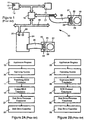
- system 10 includes a host computer module 12 (hereinafter referred to in the specification and the claims as a host computer) having system BIOS ROM 13 and system RAM 14. The system is operated using a system BIOS 15 and a translating BIOS 11 which are stored within system BIOS ROM 13.
- a host bridge 16 connects host computer 12 to an ISA bus 17 and a PCI bus 18.
- a first hard disk drive 19 is connected to ISA bus 17 using ribbon cable 20.
- Drive 19 includes disk drive firmware 21 stored in ROM 22 and disk drive controller 23 for controlling the operation of disk drive 19.
- a peripheral device, in the form of a SCSI adapter card 24 is connected to PCI bus 18 and includes a protocol translator 25 for translating all of the communications passing through adapter card 24 between the PCI protocol of the PCI bus and the protocol of the adapter card, in this case SCSI protocol.
- Adapter card 24 also includes expansion BIOS ROM 26 which contains expansion BIOS for initializing adapter card 24 during the start-up of the system.
- System 10 further includes a second hard disk drive 27 which is connected to adapter card 24.
- Disk drive 27 includes a RAM memory buffer 28, a disk drive controller 29, and disk drive firmware 30 stored within ROM 31 for controlling the operation of the hard disk drive 27.
- Hard disk drive 27 is electrically connected to adapter card 24 using ribbon cable 32. Both hard disk drive 19 and 27 are divided into cylinder, heads, sectors, and zones which specifically define each data sector within hard disk drive 19 and 27.
- system BIOS 15 checks the system first for peripheral devices connected to ISA bus 17 such as disk drive 19. In this case, when disk drive 19 is located, the system BIOS initializes disk drive 19 and configures it for use within the system.
- Hard disk drive 19 includes a RAM memory buffer 34 and the initialization process for hard disk drive 19 includes loading information such as a defect list of all of the defective memory locations on the hard disk drive from the memory storage of hard disk drive 19 into RAM memory buffer 34. This information is available for use by disk drive firmware 21 throughout the operation of disk drive 19.
- the system checks for peripheral devices connected to PCI bus 18 such as adapter card 24.
- peripheral devices such as adapter card 24.
- the system BIOS checks to see if there is any expansion BIOS associated with the adapter card. If there is expansion BIOS associated with the adapter card, in this case the expansion BIOS in expansion BIOS ROM 26, the expansion BIOS is loaded into RAM 14 and adapter card 24, along with any attached peripherals such as disk drive 27, are initialized.
- the initialization process for hard disk drive 27 includes loading information such as a defect list of all of the defective memory locations on the hard disk drive from the memory storage of hard disk drive 27 into RAM memory buffer 28 so that this information is available for use by disk drive firmware 30 throughout the operation of disk drive 27.
- the system BIOS goes on to load an operating system which is used to control the operation of the overall system.
- Firmware 21, using controller 23, translates the address information from the system BIOS into physical cylinder, head, sector, and zone address information used by the disk drive and checks a defective memory location list to make sure defective data locations are not utilized. Once these three translations are complete, controller 23 reads or writes the requested information.
- operating system 36 receives the request and determines the theoretical, or logical, address information at which operating system 36 believes the data is stored within disk drive 27.
- the expansion BIOS translates the logical address information used by operating system 36 to address information used by disk drives as indicated in box 38.
- PCI bridge 16 passes the request to protocol translator 25 on adapter card 24.
- Protocol translator 25 translates the request from PCI protocol to SCSI protocol and forwards the request to disk drive 27.
- Firmware 30, using controller 29, translates the address information into physical cylinder, head, sector, and zone address information used by the disk drive and checks the defective memory location list stored in memory buffer 28 to make sure defective data locations are not utilized. And finally, after each of these translations are complete, controller 29 reads or writes the requested information.
- the present invention provides a method for operating a mass memory storage device, such as a hard disk drive, which is connected to a host computer.
- a mass memory storage device such as a hard disk drive
- this method provides a loadable device driver including a translation mechanism which replaces all of the above described translations with a single translation performed between the operating system and the mass memory storage device.
- the arrangement allows simpler disk drive firmware to be provided on board the hard disk drive and significantly reduces the need for memory storage space such as ROM for storing the disk drive firmware.
- the invention also allows information such as defect list information to be loaded into system RAM during the start-up of the system thereby eliminating the need for RAM memory buffer space on the disk drive for storing this information for use during the operation of the disk drive.
- the combination of these novel approaches significantly reduces the cost of the hard disk drive.
- US 5,412,798 discloses a computer system having removable system resources in the form of feature cards.
- Each feature card includes a device driver having a full driver portion and a compact stub portion.
- the compact stub portion is copied into the computer system's RAM and used to link the full device driver with the operating system software of the computer system.
- a host computer which is operated using a particular operation system and a system BIOS, to operate a mass memory storage peripheral computer device, which is connected to the host computer using a peripheral bus in which relocatable expansion BIOS location addresses are allowed, the computer system further comprising a system RAM associated with the host computer, the method comprising the steps of:
- an arrangement and method are disclosed herein for operating a mass memory storage peripheral computer device connected to a host computer.
- the host computer has system RAM associated with the host computer and is operated using an operating system and a system BIOS.
- the mass memory storage peripheral computer device is connected to the host computer using a peripheral bus in which relocatable expansion BIOS location addresses are allowed.
- the arrangement and method include a loadable device driver for controlling the operation of the mass memory storage peripheral computer device during the operation of the computer system. During the start-up of the computer system, the loadable device driver is loaded into the system RAM for use during the operation of the system.
- the loadable device driver allows the host computer to communicate with and control the operation of the mass memory storage peripheral computer device in a way which does not require the system BIOS or any other type of protocol translation mechanism to be provided between the loadable device driver and the operating system or between the loadable device driver and the mass memory storage device in order for the loadable device driver to communicate with the operating system and the mass memory storage device.
- the mass memory storage peripheral computer device takes the form of a hard disk drive and the loadable device driver is stored on the hard disk drive.
- the loadable device driver includes a translating mechanism which translates data address information between (i) logical address information used by the operating system which is associated with a theoretical location of the data within a theoretical mass memory storage device and (ii) physical address information used by the actual hard disk drive.
- the physical address information is associated with the actual physical location at which the date is stored within the hard disk drive.
- the hard disk drive includes a particular number of cylinders, heads, sectors, and zones which precisely define a particular data storage area within the hard disk drive.
- the physical address information provided by the loadable device driver includes information giving the correct cylinder, head, sector, and zone within which the data is stored.
- the loadable device driver includes permanently stored defect information identifying defective memory locations of the hard disk drive.
- the loadable device driver uses the permanently stored defect information to translate the data address information between the operating system and the hard disk drive such that the defective memory locations on the hard disk drive are not utilized during the operation of the system.
- the system also includes an arrangement for detecting additional defective memory locations on the hard disk drive during any given period of operation of the hard disk drive.
- the loadable device driver includes a mechanism for storing additional defect information identifying those additional defective memory locations.
- the additional defect information is stored during the given period of operation of the hard disk drive (i) within system RAM for use by the loadable device driver and (ii) within the hard disk drive such that the additional defective memory locations become part of the permanently stored defect information and therefore is used during subsequent initializations of the hard disk drive.
- the loadable device driver uses the defect information to always access the hard disk drive at an initial non-defective address location forming part of the data address information being translated between the operating system and the hard disk drive.
- the loadable device driver also includes means, for example a pointer, for using the defect information to identify at least the first successive defective memory location which comes after the initial non-defective address location on the hard disk drive and which is associated with the data address information being translated between the operating system and the hard disk drive.
- an updated or revised version of the loadable device driver is provided on a computer memory storage medium such as a floppy disk or a compact disk. This updated version is used to update or revise the original loadable device driver which is stored within the hard disk drive.
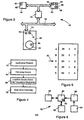
- Computer system 46 includes a host computer 48, RAM 50, a peripheral bus 52 such as a PCI bus, a host bridge 54 connecting bus 52 to host computer 48 and system RAM 50, and a mass memory storage peripheral computer device 56 having mass memory storage 58. Mass memory storage device 56 is connected to host computer 48 using peripheral bus 52.
- Host computer 48, system RAM 50, and host bridge 54 are made up of any suitable and readily providable components which allow host computer 48 and RAM 50 to be connected to peripheral bus 52 using host bridge 54. These components include, but are not limited to, any conventional 486, Pentium®, Power PC®, or RISC based components.
- host computer 48 system RAM 50, and host bridge 52 are shown having a particular configuration relative to one another, it should be understood that this is not a requirement of the present invention. Instead, these components may be interconnected in a variety of specific configurations and still remain within the scope of the invention so long as the mass memory storage peripheral computer device 56 is connected to these components using peripheral bus 52 as described hereinafter.
- Peripheral bus 52 may be any suitable and readily providable peripheral bus in which relocatable expansion BIOS location addresses are allowed.
- a peripheral bus is a PCI bus.
- PCI bus it should be understood that a wide variety of peripheral buses, such as other parallel buses, serial buses, or multiplexed buses would also fall within the scope of the present invention. If a PCI bus is utilized, the PCI specification dictates how any expansion BIOS associated with a particular peripheral computer device is loaded into RAM 50 of the host system. Other local bus configurations have corresponding specifications, and therefore, the present invention will be described in detail assuming that a PCI bus is being used to connect peripheral computer device 56 to host computer 48.
- peripheral bus will be described throughout this specification as being a PCI bus, this is not a requirement. Any peripheral bus in which relocatable expansion BIOS location addresses are allowed would equally apply.
- Host computer 48 is operated using a system BIOS 60 which is stored in a system ROM 62. After the start-up of system 46, an operating system 64 which is loaded into system RAM 50 during the start-up of the system controls the operation of the system.
- system 46 includes an arrangement for loading a loadable device driver 66 into system RAM 50 during the start-up of the system.
- Loadable device driver 66 has a translating mechanism 68 for translating data address information communicated between operating system 64 and mass memory storage device 56. Defect lists 69 may also be loaded into system RAM 50 by loadable device driver 66 during the start-up of the system.
- Loadable device driver 66 may also include access to information within defect lists 69 which identifies all of the defective memory locations within mass memory storage device 56. Loadable device driver 66 is loaded into system RAM 50 such that it is able to communicate with both operating system 64 and mass memory storage device 56 without requiring the use of system BIOS 60 or any other protocol translation mechanism between loadable device driver 66 and either operating system 64 or mass memory storage device 56. Although loadable device driver 66 does not require the presence of any other translation mechanisms between the loadable device driver and either the operating system or the mass memory storage device, it should be understood that even if other translation mechanisms are present within the system, the invention would equally apply so long as the loadable device drive is able to translate directly the data address information between the operating system and the mass memory storage device.
- Loadable device driver 66 may be stored in the conventional manner within a ROM 70 on device 56 with at least a portion of ROM 70 being expansion BIOS ROM. Using this approach, loadable device driver 66 would be loaded into system RAM 50 in the conventional manner as describe in the background of the invention. Alternatively, loadable device driver 66, along with the majority or all of the expansion BIOS associated with device 56, may be stored in memory storage 58 of device 56 and loaded into system RAM 50 as described in detail in a copending United States Patent Application, entitled METHOD AND ARRANGEMENT FOR PROVIDING BIOS TO A HOST COMPUTER, attorney docket number ITI1P001, filed October 13, 1995. Using the approach described in the referenced application, loadable device driver 66 is loaded from memory storage 58 into system RAM 50 during the start-up of the system. This approach allows the size of ROM 70 to be minimized thereby reducing the cost of device 56.
- loadable device driver may be easily updated.
- updating of the loadable device driver within ROM would require the device to be disassembled in order to replace the expansion BIOS ROM.
- using the approach of storing the loadable device driver in the mass memory storage allows the loadable device driver to be updated by simply transferring an updated version of the loadable device driver into the mass memory storage of the mass memory storage device.
- the corrected or updated version may be made available on a memory storage medium such as a floppy disk or compact disk which may be used to transfer the new version of the loadable device driver into the mass memory storage of the mass memory storage device.
- the loadable device driver may be stored in a protected portion of the mass memory storage of the device which is not user accessible.
- a utility program may be provided with the updated version of the loadable device driver which contains the appropriate mechanism to access and update the protected portion of the memory storage which contains the loadable device driver.
- mass memory storage peripheral computer device 56 is a hard disk drive and memory storage 58 is the hard disk drive memory storage.
- the hard disk drive memory storage 58 of hard disk drive 56 is divided into conventional heads, cylinders, sectors, and zones which define the specific location within memory storage 58 of each data storage location.
- Hard disk drive 56 includes a disk drive controller 72 and disk drive firmware 74 to control its operation.
- disk drive controller 72 and disk drive firmware 74 are significantly reduced in complexity relative to conventional disk drive controllers and disk drive firmware for comparable hard disk drives due to the configuration of loadable device driver 66.
- Loadable device driver 66 also sorts through defect lists 69 in system RAM 50 to identify any defective memory locations associated with the data address information being translated. These identified defective memory locations are made available to disk drive firmware 74 and disk drive controller 72 to insure that only good data sectors are utilized. Since there is no adapter card used in system 46, there is no protocol translation required and PCI bridge 54 passes the request directly to disk drive 56. As indicated in box 78, since loadable device driver 66 has already sorted defect lists 69 to identify any defective data locations and has already translated the address information into address information which is actually used by the disk drive controller 72, disk drive firmware 74 simply causes disk drive controller 72 to read or write the requested information while using the identified defective memory locations to insure that only good data sectors are utilized.
- loadable device driver 66 includes all of the information necessary to translate data address information requests from operating system 64 into address information which may be directly used by disk drive 56.
- This information includes (i) defective memory location lists 69 identifying defective data sector locations on disk drive memory storage 58 and (ii) all of the information about the physical configuration of drive 56 necessary for loadable device driver 66 to translate data address information, or logical address information, from operating system 64 into cylinder, head, sector, and zone data address information actually used by disk drive 56.
- peripheral bus such as a PCI bus, in which relocatable expansion BIOS location addresses are allowed
- all of this information may be loaded from the mass memory storage 58 of disk drive 56 into host system RAM 50 during the initialization of disk drive 56 as described in detail in the referenced application.
- this defect and physical configuration information is provided and remains within the hard disk drive itself.
- the hard disk drive controller is required to use this information to translate the CHS address information from the system BIOS to address information including zone information which can be used by the disk drive.
- the task of sorting through the defect lists and making sure only good data sectors are utilized is performed by the disk drive firmware.
- the present invention moves this information and these tasks from the disk drive to the host computer by storing all of the necessary information within host system RAM.
- the host computer RAM is used to store the entire defect lists associated with the disk drive and the information on the physical configuration of the disk drive. This eliminates the need for memory buffer space on the disk drive for storing the defect lists.
- the processor of the host computer which is much faster than the typical hard disk drive controller, is used by the loadable device driver to sort the defect lists (which are now in the host system RAM) and identify which data sectors associated with each read/write request are defective. This defect information which is specific to the particular read/write request being processed is made available to the hard disk drive. And finally, the host computer processor is used by the loadable device driver to translate the logical data address information from the operating system into actual physical data address information, including zone information, which is used directly by the disk drive controller and firmware.
- the loadable device driver (i) use-the host computer RAM to store the defect information and (ii) use the host computer processor to perform the translation and sorting tasks, in other words by shifting these tasks from the hard drive to the host computer, the cost of the hard drive may be significantly reduced.
- the memory buffer is large enough to store at least 128 sectors of data which requires at least 64K of RAM. A large portion of this memory buffer is used to store the defect lists for use by the disk drive controller throughout the operation of the disk drive. By storing the defect lists in system RAM rather than the memory buffer of the disk drive a much smaller memory buffer may be used reducing the cost of providing the necessary memory buffer.
- the disk drive controller and the disk drive firmware associated with the disk drive controller of the invention may be significantly less complex. This approach allows a less expensive disk drive controller to be used without reducing the performance of the disk drive and, because the complexity of the disk drive firmware is significantly reduced, this approach significantly reduces the ROM storage space required to store the disk drive firmware. The combination of these cost savings results in a substantial overall cost savings for a hard disk drive designed in accordance with the present invention.
- Another advantage of this approach is that only one translation needs to be performed between the operating system and the disk drive. Because the loadable device driver includes the defect information and information on the zones and the specific physical configuration of the disk drive, it is able to translate the logical data address information from the operating system directly into the actual physical data address information used by the disk drive. In the conventional approach illustrated in Figure 2, the system BIOS or translating BIOS translates the logical data address information from the operating system into CHS data address information according to the disk drive industry standards.
- the firmware of the disk drive itself must perform another level of translation in order to determine the actual physical data storage location and then use this actual data storage location to cause the disk drive controller to read or write the requested data.
- the approach of the invention speeds up the overall process of handling a read/write request from the operating system and the disk drive and improves the performance of the overall system.
- the loadable device driver of the present invention may take on a wide variety of specific forms and still remain within the scope of the present invention. These forms may be specific to a particular peripheral bus (such as a PCI bus), to other computer architectures (such as a certain processor), and to particular mass memory storage devices (such as a specific model of a hard disk drive). Also, since the loadable device driver of the present invention communicates directly with the mass memory storage device without requiring the use of the system BIOS, a wide variety of protocols may be used for the communication between the loadable device driver and the mass memory storage device. These protocols do not need to conform to the constraints of the system BIOS and therefore a protocol may be used which maximizes the performance of the particular mass memory storage device associated with the loadable device driver.
- loadable device driver 66 includes a pointer 80 associated with defect lists 69.
- defect lists 69 contain a list of all of the defective memory locations for hard disk drive 56.
- Figure 5 illustrates in tabular form an example of a portion of such a defect list. In this list the letters A-E in the leftmost column represent pointer addresses which identify a specific location within the defect list. The second, third, and fourth columns correspond to the specific cylinder, head, and sector of each of the defective memory locations.
- loadable device driver 66 when loadable device driver 66 receives a read/write request which includes the amount of data requested from operating system 64, it uses the defect list to identify the known good memory location associated with the beginning of the data being requested. Loadable device driver 66 then sorts through the defect list and identifies the first defective memory location following the known good beginning data memory location. Pointer 80 is assigned the pointer address corresponding to this first defective memory location. Loadable device driver 66 then sends the pointer address of the first defect to disk drive firmware 74 of disk drive 56 along with the data address information at which drive controller 72 is to begin reading/writing data and the amount of data disk drive controller 72 should read/write. Disk drive firmware 74 uses pointer 80 to obtain the defective memory locations which are associated with the read/write request from loadable device driver 66 without requiring disk drive firmware 74 to sort through the entire defect list.
- loadable device driver 66 receives a read request from operating system 64.
- Loadable device driver 66 determines that the read request corresponds to ten sectors of data stored beginning at the known good memory storage location of cylinder 23, head 1, and sector 1. Using this memory storage location address, loadable device driver 66 sorts through the defect list to identify the next successive memory location that is defective. In this case, the next successive memory location that is defective is the location which corresponds to cylinder 23, head 1, and sector 2. Since this defective memory location is assigned pointer address C as shown in Figure 5, loadable device driver 66 provides disk drive firmware 74 with the pointer address C along with the read request for ten sectors of data beginning at the location of cylinder 23, head 1, and sector 1.
- disk drive firmware 74 uses pointer 80 to obtain a predetermined number of the successive defective memory locations from defect lists 69 in host RAM beginning with the defective memory location indicated by pointer 80. In this case, only the first defective location which corresponds to pointer address C is relevant to the information being read, however, in other specific situations there may be many defective memory locations associated with the data to be read. Disk drive firmware 74 uses these defective memory locations which are specific to the data being read to cause disk drive controller 72 to skip the defective memory locations and insure that only good data sectors are utilized.
- the invention is not limited to this specific embodiment.
- the particular protocol used to provide this function may take on a wide variety of specific forms and still remain within the scope of the present invention. This is also the case for other functions and/or data which may be moved from the disk drive firmware of the disk drive to the system RAM.
- the loadable device driver of the present invention since the loadable device driver of the present invention communicates directly with the mass memory storage device without requiring the use of the system BIOS, a wide variety of protocols may be used for the communication between the loadable device driver and the mass memory storage device. These protocols do not need to conform to the constraints of the system BIOS and therefore a protocol may be used which maximizes the performance of the particular mass memory storage device associated with the loadable device driver.
- the loadable device driver of the present invention has been described above as including a list of the defective memory locations of the mass memory storage device and information on the specific configuration of the device so that the loadable device driver is able to perform the translating function and the function of sorting through the defect list.
- this general approach of moving certain functions and/or data from the device to the host computer by using the loadable device driver to perform these functions may include a variety of other functions. By moving these other functions and/or data to the host computer using the loadable device driver, the complexity of the drive may be further reduced resulting in further cost savings.
- some examples of the functions which may be moved from a conventional disk drive controller to the host system using the loadable device driver of the invention are; (i) detecting new defective memory locations and adding these new defective locations to both the permanent defect lists stored on the memory storage of the mass memory storage and the defect lists within the host RAM for use during the operation of the system, (ii) determining chip settings for the disk drive controller based on the known configuration of the device and providing read channel information to the disk drive controller, and (iii) allocating host system RAM rather than RAM provided on the disk drive for use as read/write cache.
- system 46 would include an arrangement for detecting and confirming data errors. If it is determined using these methods that these data errors are the result of newly found, additional defective memory locations or damage to the associated data sector on disk drive 56, loadable device driver 66 adds the newly found, additional defective memory location to defect lists 69 within host system RAM 50. However, in order to permanently add the newly found, additional defective memory location to the defect lists, loadable device drive 66 also adds the newly found defective memory location to the permanent defect lists stored in the mass memory storage 58 of mass memory storage device 56.
- loadable device driver 66 may include an arrangement, such as a utility program, which allows the loadable device drive to access the portion of the memory containing the permanent defect lists thereby allowing the loadable device driver to add the newly found defective memory location to the defect lists.
- the disk drive firmware which controls the operation of the drive controller typically includes information on various settings which are used to control the drive controller.
- One example of this is the various data read/write rates associated with the different zones of the disk drive.
- the function of providing these chip settings or settings for controlling the operation of the drive controller may be included as part of the functions and/or data loaded into host system RAM. If this is the case, still referring to Figure 3, loadable device driver 66 uses the information on the specific configuration of the disk drive included within loadable device driver 66 to determine, based on the read/write request from operating system 64, which zone of the disk drive the read/write request is associated with.
- loadable device driver 66 determines the proper settings for drive controller 72 and includes the proper commands with the read/write request to set drive controller 72 to the proper settings. Furthermore, if the read/write request includes data which involves data sectors in more than one zone, disk drive firmware 74 determines at what point within the requested data the zone changes from one zone to another and reads from system RAM 50 the appropriate chip settings.
- controller settings for different zones has been used as an example, it should be understood that this same approach would apply to other specific operating parameters all of which would fall within the scope of the invention.
- the third example of functions which may be moved from the disk drive to the loadable device driver is the example of the read/write cache.
- a fairly large RAM memory buffer is provided as part of the disk drive.
- a portion of this RAM memory buffer is used as a read ahead memory cache.
- the present invention allows this function to be moved from the disk drive to the loadable device driver. By doing this, host system RAM may be used to provide the memory space for the read ahead memory cache thereby reducing the amount of memory buffer RAM necessary within the disk drive.
- loadable device driver 66 receives a read request from operating system 64, it determines how much additional data will be read into a read ahead cache.
- Loadable device driver 66 obtains space within system RAM 50 for storing this additional data and instructs drive controller 72 to read not only the requested data but also the additional data which loadable device driver 66 stores in the memory space obtained within system RAM 50. This approach not only reduces the need for RAM memory buffer space, but also improves the performance of the system. By storing the read ahead cache in the system RAM, it may be accessed by the host system without having to access in any way the disk drive. Also, since loadable device driver 66 has information on the specific configuration of disk drive 56, it may be arranged to take advantage of this information in order to more effectively read ahead by reading data which may not necessarily be the next successive data on disk drive 56.
- System 82 includes a host computer module 84 having system RAM 86 and includes a particular peripheral computer device 88 connected to host computer module 84 and RAM 86 through a suitable and compatible bus (not shown). Peripheral computer device 88 requires certain operating parameters 90 for its operation. System 82 further includes an arrangement 92 for loading operating parameters 90 from a source 94 into system RAM 86 during the start-up of the system and for allowing the system to use operating parameters 90 during the operation of the system to control the operation of peripheral computer device 88.
- Arrangement 92 may be provided as part of a loadable device driver such as the loadable device driver described in detail for the previously described embodiments.
- the operating parameters may be loaded as part of an expansion BIOS associated with the particular peripheral computer device.
- This expansion BIOS may be at least partially stored in a mass memory storage device connected to the system in the manner described in detail in the referenced patent.
- Source 94 may be ROM provided on board the particular peripheral computer device 88 itself, or any other source such as mass memory storage on a mass memory storage peripheral computer device connected to the system.
- Some examples of mass memory storage devices which may be used as source 94 are hard disk drives, compact disk drives, tape drives, or floppy disk drives.
- system 82 has access to operating parameters 90 stored in RAM 86 such that system 82 may use operating parameters 90 to control the operation of particular peripheral device 88.
- These operating parameters may be used by peripheral device 88 itself to control its own operation.
- the device may be a hard disk drive and the operating parameters may be the defect list identifying the defective memory locations on the disk drive.
- host computer 84 may use operating parameters 90 to control the operation of peripheral device 88. This approach of storing the operating parameters for peripheral devices in the system RAM reduces or eliminates the need for providing certain memory space on the peripheral device. These savings significantly reduce the cost of providing the particular peripheral computer device.
- the operating parameters may be the defect lists, chip settings for the controller of the device, or read ahead cache.
- the operating parameters would be data and/or code specific to these other devices.
- this general approach may be applied to a wide variety of peripheral computer devices as well as a wide variety of specific operating parameters for any one of these variety of peripheral computer devices. The present invention would equally apply to any combination of these, so long as operating parameters associated with a particular computer device are stored within the system RAM for use by the system.
- peripheral bus has been described in the earlier embodiments as being a PCI bus, this is not a requirement. As mentioned above, any peripheral bus which allows relocatable expansion BIOS location addresses are allowed would equally apply. In fact, for the general approach of moving operating parameters required for the operation of a particular peripheral device from the peripheral device to system RAM, the peripheral bus may be any bus which allows the operating parameters to be stored in system RAM during the start-up of the system. Also, although the mass memory storage device has been described throughout as a hard disk drive, the invention would equally apply to other mass memory storage devices such as compact disk drives, tape drives, or floppy disk drives.
- addressing scheme for addressing the mass memory storage devices has been described throughout as using a CHS or cylinder, head, sector, and zone addressing scheme, this is not a requirement. Instead, any addressing scheme including, but not limited to, linear addressing schemes (such as those used by CD players) or holographic addressing schemes using XYZ coordinates to define memory locations would also fall within the scope of the invention. Therefore, the present examples are to be considered as illustrative and not restrictive, and the invention is not to be limited to the details given herein, but may be modified within the scope of the appended claims.
Landscapes
- Engineering & Computer Science (AREA)
- Theoretical Computer Science (AREA)
- Physics & Mathematics (AREA)
- General Engineering & Computer Science (AREA)
- General Physics & Mathematics (AREA)
- Software Systems (AREA)
- Quality & Reliability (AREA)
- Human Computer Interaction (AREA)
- Computer Security & Cryptography (AREA)
- Memory System Of A Hierarchy Structure (AREA)
- Stored Programmes (AREA)
- Signal Processing For Digital Recording And Reproducing (AREA)
Abstract
Claims (15)
- Procédé permettant à un ordinateur central (48) qui est exploité en utilisant un système d'exploitation particulier (64) et un BIOS (60) de système d'exploiter un dispositif informatique périphérique (56) de stockage en mémoire de masse qui est connecté à l'ordinateur central par l'utilisation d'un bus périphérique (52) dans lequel des adresses relogeables d'emplacement de BIOS d'extension sont autorisées, le système informatique comprenant en outre une mémoire RAM (50) de système associée à l'ordinateur central, le procédé comprenant les étapes de :a) fournir un gestionnaire (66) de dispositifs pouvant être chargé comprenant des moyens de traduction d'adresse pour traduire des informations d'adresse de données échangées entre le système (64) d'exploitation et le dispositif informatique périphérique (56) de stockage en mémoire de masse ;b) pendant le démarrage du système, charger le gestionnaire (66) de dispositifs pouvant être chargé dans la mémoire RAM (50) de système pour une utilisation pendant l'exploitation du système,
dans lequel le gestionnaire (66) de dispositifs pouvant être chargé est en communication avec le système d'exploitation sans nécessiter l'utilisation du BIOS de système, de traduction de protocole ni tout autre type de mécanisme de traduction d'adresse de données entre le gestionnaire de dispositif pouvant être chargé et le dispositif de stockage en mémoire de masse ; etc) utiliser les moyens de traduction du gestionnaire de dispositifs pouvant être chargé, traduire des informations d'adresse de données échangées entre le système d'exploitation (64) et le dispositif informatique périphérique (56) de stockage en mémoire de masse pendant le fonctionnement du système. - Procédé selon la revendication 1, dans lequel l'étape de chargement du gestionnaire (66) de dispositif pouvant être chargé comprend l'étape de chargement du gestionnaire de dispositifs pouvant être chargé de sorte que le gestionnaire de dispositifs pouvant être chargé soit en communication directe avec le dispositif informatique périphérique (56) de stockage en mémoire de masse sans aucun mécanisme de traduction entre le gestionnaire de dispositif pouvant être chargé et le dispositif informatique périphérique de stockage en mémoire de masse.
- Procédé selon la revendication 1 ou 2, dans lequel l'étape de traduction d'informations d'adresse de données comprend l'étape de traduction d'informations d'adresse de données entre(i) des informations d'adresse logique utilisées par le système d'exploitation (64) qui sont associées à un emplacement théorique des données dans un dispositif théorique de stockage en mémoire de masse et(ii) des informations d'adresse physique utilisées par le dispositif informatique périphérique (56) de stockage en mémoire de masse, les informations d'adresse physique étant associées à l'emplacement physique réel dans lequel les données sont stockées dans le stockage en mémoire de masse du dispositif informatique périphérique de stockage en mémoire de masse.
- Procédé selon l'une quelconque des revendications 1 à 3, dans lequel le bus périphérique (52) utilisé pour relier le dispositif informatique périphérique (56) de stockage en mémoire de masse à l'ordinateur central (48) est un bus PCI et dans lequel le système utilise le protocole PCI pour utiliser le bus PCI.
- Procédé selon l'une quelconque des revendications 1 à 3, dans lequel le bus (52) de périphérique utilisé pour relier le dispositif informatique périphérique (56) de stockage en mémoire de masse à l'ordinateur central (48) est un bus série, et dans lequel le système utilise un protocole particulier pour utiliser le bus série.
- Procédé selon l'une quelconque des revendications précédentes, dans lequel :a) l'étape de fourniture du gestionnaire de dispositif pouvant être chargé comprend l'étape de chargement du gestionnaire (66) de dispositifs pouvant être chargé qui est stocké dans le stockage en mémoire de masse du dispositif informatique périphérique (56) de stockage en mémoire de masse, etb) l'étape de chargement du gestionnaire de dispositif pouvant être chargé comprend l'étape de chargement du gestionnaire de dispositif pouvant être chargé depuis le dispositif informatique périphérique (56) de stockage en mémoire de masse vers la mémoire RAM (50) de système pendant le démarrage du système pour une utilisation pendant le fonctionnement du système.
- Procédé selon la revendication 6, dans lequel le dispositif informatique périphérique (56) de stockage en mémoire de masse est une unité (58) de disque dur, et dans lequel l'étape de fourniture du gestionnaire de dispositif pouvant être chargé comprend l'étape de fourniture d'un gestionnaire de dispositifs pouvant être chargé stocké dans la mémoire de masse de l'unité de disque dur.
- Procédé selon la revendication 7, dans lequel l'étape de fourniture du gestionnaire de dispositif pouvant être chargé comprend l'étape de fourniture d'un gestionnaire (66) de dispositif pouvant être chargé stocké dans une portion de stockage en mémoire de masse du lecteur de disque fixe qui n'est pas accessible à l'utilisateur.
- Procédé selon la revendication 7 ou la revendication 8 dans la mesure où elles dépendent de la revendication 3, dans lequel l'unité (58) de disque dur comprend un nombre particulier de cylindres, de têtes, de secteurs et de zones qui définissent avec précision une région particulière de stockage de données dans le stockage en mémoire de masse de l'unité (58) de disque dur, et dans lequel l'étape de traduction d'informations d'adresse de données entre des informations d'adresse logique et des informations d'adresse physique comprend l'étape de traduction d'informations d'adresse de données entre des informations d'adresse logique et des informations d'adresse physique donnant correctement le cylindre, la tête, le secteur, et la zone dans lesquels sont stockées les données sur le stockage en mémoire de masse de l'unité de disque dur.
- Procédé selon l'une quelconque des revendications 7 à 9, dans lequel l'étape de fourniture d'un gestionnaire de dispositifs pouvant être chargé comprend l'étape de fourniture d'un gestionnaire de dispositifs pouvant être chargé qui comprend des informations de défaut stocké en permanence identifiant des emplacements défectueux de mémoire sur le stockage en mémoire de masse de l'unité de disque dur et dans lequel l'étape de traduction d'informations d'adresse de données comprend l'étape d'utilisation des informations de défaut stockées en permanence pour traduire les informations d'adresse de données entre le système d'exploitation (64) et le dispositif (56) de stockage en mémoire de masse, de sorte que les emplacements défectueux de mémoire sur le dispositif de stockage en mémoire de masse ou l'unité de disque dur ne soient pas utilisés pendant le fonctionnement du système.
- Procédé selon la revendication 10, comprenant en outre les étapes consistant à :a) détecter des emplacements défectueux supplémentaires de mémoire sur le stockage en mémoire de masse du lecteur de disque fixe pendant une période donnée de fonctionnement de l'unité (58) de disque dur, etb) stocker des informations supplémentaires de défaut identifiant ces emplacements défectueux supplémentaires de mémoire pendant la période donnée de fonctionnement de l'unité (58) de disque dur(i) dans la mémoire RAM (50) de système pour une utilisation par le gestionnaire (66) de dispositifs pouvant être chargé et(ii) dans l'unité (58) de disque dur de sorte que de tels emplacements défectueux supplémentaires de mémoire fassent partie des informations de défaut stockées en permanence.
- Procédé selon la revendication 10 ou la revendication 11, comprenant en outre les étapes consistant à :a) utiliser les informations de défaut stockées en permanence et les moyens de traduction accédant au stockage en mémoire de masse de l'unité (58) de disque dur à un emplacement initial non défectueux d'adresse faisant partie des informations d'adresse de données qui sont traduites entre le système d'exploitation (64) et l'unité (58) de disque dur ;b) fournir des moyens pour identifier au moins le premier emplacement de mémoire défectueux qui suit sur le stockage en mémoire de masse de l'unité de disque dur qui est associé aux informations d'adresse de données qui sont traduites entre le système d'exploitation (64) et l'unité (58) de disque dur ; etc) utiliser les moyens pour indiquer les emplacements de mémoire défectueux, traduire les informations d'adresse de données échangées entre le système d'exploitation et le dispositif informatique périphérique de stockage en mémoire de masse pendant le fonctionnement du système, de sorte que les emplacements de mémoire défectueux sur le stockage en mémoire de masse de l'unité de disque dur ne soient pas utilisés pendant le fonctionnement du système.
- Procédé selon la revendication 10, comprenant en outre l'étape de chargement de paramètres supplémentaires d'exploitation associés au dispositif informatique périphérique (56) de stockage en mémoire de masse provenant du dispositif périphérique de stockage en mémoire de masse vers la mémoire RAM (50) de système pendant le démarrage du système pour que le système les utilise pour faire fonctionner le dispositif périphérique (56) de stockage en mémoire de masse.
- Procédé selon la revendication 13, dans lequel le dispositif informatique périphérique (56) de stockage en mémoire de masse comprend un dispositif de commande pour commander les fonctions de stockage en mémoire du dispositif de stockage en mémoire de masse, et dans lequel l'étape de chargement des paramètres supplémentaires d'exploitation dans la mémoire RAM (50) de système comprend l'étape de chargement dans la mémoire RAM de système de réglages pour le dispositif de commande.
- Procédé selon la revendication 13, dans lequel l'étape de chargement des paramètres supplémentaires d'exploitation pendant le démarrage du système comprend l'étape d'affectation d'une portion de la mémoire RAM (50) de système pour une utilisation par le dispositif informatique périphérique (56) de stockage en mémoire de masse pendant le fonctionnement du système en tant que mémoire cache à lecture anticipée.
Applications Claiming Priority (3)
| Application Number | Priority Date | Filing Date | Title |
|---|---|---|---|
| US553024 | 1995-11-03 | ||
| US08/553,024 US6393492B1 (en) | 1995-11-03 | 1995-11-03 | Method and arrangement for operating a mass memory storage peripheral computer device connected to a host computer |
| PCT/US1996/017550 WO1997018505A2 (fr) | 1995-11-03 | 1996-10-31 | Procede et agencement permettant de faire fonctionner un dispositif informatique peripherique de stockage d'une memoire de grande capacite connecte a un ordinateur central |
Publications (3)
| Publication Number | Publication Date |
|---|---|
| EP0806005A2 EP0806005A2 (fr) | 1997-11-12 |
| EP0806005A4 EP0806005A4 (fr) | 1999-01-20 |
| EP0806005B1 true EP0806005B1 (fr) | 2003-03-26 |
Family
ID=24207800
Family Applications (1)
| Application Number | Title | Priority Date | Filing Date |
|---|---|---|---|
| EP96937864A Expired - Lifetime EP0806005B1 (fr) | 1995-11-03 | 1996-10-31 | Procede et agencement permettant de faire fonctionner un dispositif informatique peripherique de stockage d'une memoire de grande capacite connecte a un ordinateur central |
Country Status (5)
| Country | Link |
|---|---|
| US (1) | US6393492B1 (fr) |
| EP (1) | EP0806005B1 (fr) |
| AU (1) | AU7551496A (fr) |
| DE (1) | DE69626962T2 (fr) |
| WO (1) | WO1997018505A2 (fr) |
Families Citing this family (22)
| Publication number | Priority date | Publication date | Assignee | Title |
|---|---|---|---|---|
| US5991841A (en) * | 1997-09-24 | 1999-11-23 | Intel Corporation | Memory transactions on a low pin count bus |
| US6212588B1 (en) * | 1998-03-09 | 2001-04-03 | Texas Instruments Incorporated | Integrated circuit for controlling a remotely located mass storage peripheral device |
| SG90038A1 (en) * | 1998-03-09 | 2002-07-23 | Texas Instruments Inc | Mass storage peripheral device with associated personality rom |
| US6195216B1 (en) * | 1998-03-09 | 2001-02-27 | Texas Instruments Incorporated | Mass storage peripheral device with operating circuitry and programs located remotely therefrom |
| US6694354B1 (en) * | 1998-11-30 | 2004-02-17 | Telefonaktiebolaget Lm Ericsson (Publ) | Host computer access to peripheral device drivers |
| JP3812928B2 (ja) * | 1999-07-14 | 2006-08-23 | 株式会社日立製作所 | 外部記憶装置及び情報処理システム |
| US6567911B1 (en) * | 1999-12-06 | 2003-05-20 | Adaptec, Inc. | Method of conserving memory resources during execution of system BIOS |
| US7237101B1 (en) * | 2000-02-12 | 2007-06-26 | International Business Machines Corporation | Methods and apparatus for self describing devices |
| JP4649009B2 (ja) * | 2000-03-08 | 2011-03-09 | 株式会社東芝 | カードインタフェースを備えた情報処理装置、同装置に装着可能なカード型電子機器、及び同装置におけ動作モード設定方法 |
| US6560641B1 (en) * | 2000-03-29 | 2003-05-06 | Unisys Corporation | System, method, and adapter card for remote console emulation including remote control of a peripheral device |
| JP2002063042A (ja) * | 2000-08-21 | 2002-02-28 | Nec Microsystems Ltd | プログラム・モジュール管理システム、その管理方法及びその管理プログラムを記録した記録媒体 |
| JP2004302991A (ja) * | 2003-03-31 | 2004-10-28 | Giga-Byte Technology Co Ltd | コンピュータシステム用インターフェイスbiosのバックアップ方法 |
| US7536558B2 (en) * | 2003-08-29 | 2009-05-19 | Tgbw Inc. | Flash memory distribution of digital content |
| US7434019B2 (en) * | 2003-09-18 | 2008-10-07 | Seagate Technology Llc | Method and apparatus for managing buffer random access memory |
| US20050071624A1 (en) * | 2003-09-29 | 2005-03-31 | Rothman Michael A. | Providing a self-describing media for a computer system |
| JP2006301771A (ja) * | 2005-04-18 | 2006-11-02 | Toshiba Corp | 情報処理装置および動作制御方法 |
| US8631221B2 (en) * | 2008-02-22 | 2014-01-14 | Cisco Technology, Inc. | Method and apparatus for allocating host memory for a memory-less add-on devices |
| US8307180B2 (en) | 2008-02-28 | 2012-11-06 | Nokia Corporation | Extended utilization area for a memory device |
| US8874824B2 (en) | 2009-06-04 | 2014-10-28 | Memory Technologies, LLC | Apparatus and method to share host system RAM with mass storage memory RAM |
| US9417998B2 (en) | 2012-01-26 | 2016-08-16 | Memory Technologies Llc | Apparatus and method to provide cache move with non-volatile mass memory system |
| US9311226B2 (en) | 2012-04-20 | 2016-04-12 | Memory Technologies Llc | Managing operational state data of a memory module using host memory in association with state change |
| WO2015089488A1 (fr) | 2013-12-12 | 2015-06-18 | Memory Technologies Llc | Modules de mémorisation optimisée à canaux |
Family Cites Families (5)
| Publication number | Priority date | Publication date | Assignee | Title |
|---|---|---|---|---|
| US5371885A (en) | 1989-08-29 | 1994-12-06 | Microsoft Corporation | High performance file system |
| US5237689A (en) * | 1990-05-31 | 1993-08-17 | Hewlett-Packard Company | Configuration of mass storage devices |
| US5179666A (en) * | 1990-06-07 | 1993-01-12 | Unisys Corporation | Block oriented peripheral device interface |
| US5319751A (en) | 1991-12-27 | 1994-06-07 | Intel Corporation | Device driver configuration in a computer system |
| US5355498A (en) * | 1992-02-25 | 1994-10-11 | Sun Microsystems, Inc. | Method and apparatus for booting a computer system without loading a device driver into memory |
-
1995
- 1995-11-03 US US08/553,024 patent/US6393492B1/en not_active Expired - Lifetime
-
1996
- 1996-10-31 WO PCT/US1996/017550 patent/WO1997018505A2/fr not_active Ceased
- 1996-10-31 EP EP96937864A patent/EP0806005B1/fr not_active Expired - Lifetime
- 1996-10-31 AU AU75514/96A patent/AU7551496A/en not_active Abandoned
- 1996-10-31 DE DE69626962T patent/DE69626962T2/de not_active Expired - Lifetime
Also Published As
| Publication number | Publication date |
|---|---|
| EP0806005A4 (fr) | 1999-01-20 |
| US6393492B1 (en) | 2002-05-21 |
| DE69626962D1 (de) | 2003-04-30 |
| EP0806005A2 (fr) | 1997-11-12 |
| AU7551496A (en) | 1997-06-05 |
| WO1997018505A2 (fr) | 1997-05-22 |
| WO1997018505A3 (fr) | 1997-06-12 |
| DE69626962T2 (de) | 2003-12-18 |
Similar Documents
| Publication | Publication Date | Title |
|---|---|---|
| US5875349A (en) | Method and arrangement for allowing a computer to communicate with a data storage device | |
| EP0806005B1 (fr) | Procede et agencement permettant de faire fonctionner un dispositif informatique peripherique de stockage d'une memoire de grande capacite connecte a un ordinateur central | |
| US7424593B2 (en) | Increasing the memory performance of flash memory devices by writing sectors simultaneously to multiple flash memory devices | |
| US5835760A (en) | Method and arrangement for providing BIOS to a host computer | |
| US6202138B1 (en) | Increasing the memory performance of flash memory devices by writing sectors simultaneously to multiple flash memory devices | |
| US6757800B1 (en) | Increasing the memory performance of flash memory devices by writing sectors simultaneously to multiple flash memory devices | |
| US5742934A (en) | Flash solid state disk card with selective use of an address conversion table depending on logical and physical sector numbers | |
| US5150465A (en) | Mode-selectable integrated disk drive for computer | |
| EP1133730B1 (fr) | Procede de programmation flash d'une puce de memoire rom d'un adaptateur hote avec un code bios mis a jour | |
| US5966732A (en) | Method and apparatus for adding to the reserve area of a disk drive | |
| US7639538B2 (en) | Memory card, semiconductor device, and method of controlling memory card | |
| US5768584A (en) | ROM chip enable encoding method and computer system employing the same | |
| EP0631241A1 (fr) | Initialisation d'un réseau à bus multiples | |
| JPH04218828A (ja) | 大容量磁気ディスク駆動装置 | |
| US6693754B2 (en) | Method and apparatus for a disc drive adaptive file system | |
| US7245539B2 (en) | Memory card, semiconductor device, and method of controlling semiconductor memory | |
| US6738879B2 (en) | Advanced technology attachment compatible disc drive write protection scheme | |
| US6430660B1 (en) | Unified memory hard disk drive system | |
| KR100222908B1 (ko) | 플래시 메모리 시스템 | |
| US20020083225A1 (en) | Recordable disk recording controller with batch register controller | |
| US6223241B1 (en) | Sharing of the indirect addressing of the registers of a peripheral dedicated to emulation | |
| KR20030091498A (ko) | 데이터 저장 시스템 | |
| JPH0728700A (ja) | 記憶装置 | |
| JP2002318779A (ja) | デバイス装置とそのレジスタのアクセス方法 | |
| JPH06290547A (ja) | ディスク装置の高速データ転送方法 |
Legal Events
| Date | Code | Title | Description |
|---|---|---|---|
| PUAI | Public reference made under article 153(3) epc to a published international application that has entered the european phase |
Free format text: ORIGINAL CODE: 0009012 |
|
| AK | Designated contracting states |
Kind code of ref document: A2 Designated state(s): DE FR GB IT NL |
|
| 17P | Request for examination filed |
Effective date: 19971211 |
|
| A4 | Supplementary search report drawn up and despatched |
Effective date: 19981204 |
|
| AK | Designated contracting states |
Kind code of ref document: A4 Designated state(s): DE FR GB IT NL |
|
| 17Q | First examination report despatched |
Effective date: 20010410 |
|
| RAP1 | Party data changed (applicant data changed or rights of an application transferred) |
Owner name: TEXAS INSTRUMENTS INCORPORATED |
|
| GRAH | Despatch of communication of intention to grant a patent |
Free format text: ORIGINAL CODE: EPIDOS IGRA |
|
| GRAH | Despatch of communication of intention to grant a patent |
Free format text: ORIGINAL CODE: EPIDOS IGRA |
|
| GRAA | (expected) grant |
Free format text: ORIGINAL CODE: 0009210 |
|
| AK | Designated contracting states |
Designated state(s): DE FR GB IT NL |
|
| PG25 | Lapsed in a contracting state [announced via postgrant information from national office to epo] |
Ref country code: NL Free format text: LAPSE BECAUSE OF FAILURE TO SUBMIT A TRANSLATION OF THE DESCRIPTION OR TO PAY THE FEE WITHIN THE PRESCRIBED TIME-LIMIT Effective date: 20030326 Ref country code: IT Free format text: LAPSE BECAUSE OF FAILURE TO SUBMIT A TRANSLATION OF THE DESCRIPTION OR TO PAY THE FEE WITHIN THE PRESCRIBED TIME-LIMIT;WARNING: LAPSES OF ITALIAN PATENTS WITH EFFECTIVE DATE BEFORE 2007 MAY HAVE OCCURRED AT ANY TIME BEFORE 2007. THE CORRECT EFFECTIVE DATE MAY BE DIFFERENT FROM THE ONE RECORDED. Effective date: 20030326 Ref country code: FR Free format text: LAPSE BECAUSE OF FAILURE TO SUBMIT A TRANSLATION OF THE DESCRIPTION OR TO PAY THE FEE WITHIN THE PRESCRIBED TIME-LIMIT Effective date: 20030326 |
|
| REG | Reference to a national code |
Ref country code: GB Ref legal event code: FG4D |
|
| REF | Corresponds to: |
Ref document number: 69626962 Country of ref document: DE Date of ref document: 20030430 Kind code of ref document: P |
|
| NLV1 | Nl: lapsed or annulled due to failure to fulfill the requirements of art. 29p and 29m of the patents act | ||
| PGFP | Annual fee paid to national office [announced via postgrant information from national office to epo] |
Ref country code: FR Payment date: 20031003 Year of fee payment: 8 |
|
| PLBE | No opposition filed within time limit |
Free format text: ORIGINAL CODE: 0009261 |
|
| STAA | Information on the status of an ep patent application or granted ep patent |
Free format text: STATUS: NO OPPOSITION FILED WITHIN TIME LIMIT |
|
| EN | Fr: translation not filed | ||
| 26N | No opposition filed |
Effective date: 20031230 |
|
| PGFP | Annual fee paid to national office [announced via postgrant information from national office to epo] |
Ref country code: DE Payment date: 20101029 Year of fee payment: 15 |
|
| PGFP | Annual fee paid to national office [announced via postgrant information from national office to epo] |
Ref country code: GB Payment date: 20110930 Year of fee payment: 16 |
|
| GBPC | Gb: european patent ceased through non-payment of renewal fee |
Effective date: 20121031 |
|
| PG25 | Lapsed in a contracting state [announced via postgrant information from national office to epo] |
Ref country code: GB Free format text: LAPSE BECAUSE OF NON-PAYMENT OF DUE FEES Effective date: 20121031 Ref country code: DE Free format text: LAPSE BECAUSE OF NON-PAYMENT OF DUE FEES Effective date: 20130501 |
|
| REG | Reference to a national code |
Ref country code: DE Ref legal event code: R119 Ref document number: 69626962 Country of ref document: DE Effective date: 20130501 |