EP0805548A2 - Power factor correction circuit - Google Patents
Power factor correction circuit Download PDFInfo
- Publication number
- EP0805548A2 EP0805548A2 EP97300443A EP97300443A EP0805548A2 EP 0805548 A2 EP0805548 A2 EP 0805548A2 EP 97300443 A EP97300443 A EP 97300443A EP 97300443 A EP97300443 A EP 97300443A EP 0805548 A2 EP0805548 A2 EP 0805548A2
- Authority
- EP
- European Patent Office
- Prior art keywords
- voltage
- output
- digital
- pulse width
- circuit
- Prior art date
- Legal status (The legal status is an assumption and is not a legal conclusion. Google has not performed a legal analysis and makes no representation as to the accuracy of the status listed.)
- Granted
Links
- 230000002238 attenuated effect Effects 0.000 claims abstract description 14
- 238000000034 method Methods 0.000 claims description 6
- 230000003247 decreasing effect Effects 0.000 claims 1
- 230000000737 periodic effect Effects 0.000 claims 1
- 239000003990 capacitor Substances 0.000 description 5
- 238000010586 diagram Methods 0.000 description 3
- 238000004519 manufacturing process Methods 0.000 description 3
- 230000010355 oscillation Effects 0.000 description 2
- 230000009471 action Effects 0.000 description 1
- 230000008859 change Effects 0.000 description 1
- 238000010276 construction Methods 0.000 description 1
- 230000001419 dependent effect Effects 0.000 description 1
- 238000005516 engineering process Methods 0.000 description 1
- 238000001914 filtration Methods 0.000 description 1
- 230000008569 process Effects 0.000 description 1
- 230000009467 reduction Effects 0.000 description 1
- 230000004044 response Effects 0.000 description 1
- 230000003019 stabilising effect Effects 0.000 description 1
Images
Classifications
-
- H—ELECTRICITY
- H03—ELECTRONIC CIRCUITRY
- H03K—PULSE TECHNIQUE
- H03K5/00—Manipulating of pulses not covered by one of the other main groups of this subclass
-
- H—ELECTRICITY
- H02—GENERATION; CONVERSION OR DISTRIBUTION OF ELECTRIC POWER
- H02M—APPARATUS FOR CONVERSION BETWEEN AC AND AC, BETWEEN AC AND DC, OR BETWEEN DC AND DC, AND FOR USE WITH MAINS OR SIMILAR POWER SUPPLY SYSTEMS; CONVERSION OF DC OR AC INPUT POWER INTO SURGE OUTPUT POWER; CONTROL OR REGULATION THEREOF
- H02M1/00—Details of apparatus for conversion
- H02M1/42—Circuits or arrangements for compensating for or adjusting power factor in converters or inverters
- H02M1/4208—Arrangements for improving power factor of AC input
- H02M1/4225—Arrangements for improving power factor of AC input using a non-isolated boost converter
-
- Y—GENERAL TAGGING OF NEW TECHNOLOGICAL DEVELOPMENTS; GENERAL TAGGING OF CROSS-SECTIONAL TECHNOLOGIES SPANNING OVER SEVERAL SECTIONS OF THE IPC; TECHNICAL SUBJECTS COVERED BY FORMER USPC CROSS-REFERENCE ART COLLECTIONS [XRACs] AND DIGESTS
- Y02—TECHNOLOGIES OR APPLICATIONS FOR MITIGATION OR ADAPTATION AGAINST CLIMATE CHANGE
- Y02B—CLIMATE CHANGE MITIGATION TECHNOLOGIES RELATED TO BUILDINGS, e.g. HOUSING, HOUSE APPLIANCES OR RELATED END-USER APPLICATIONS
- Y02B70/00—Technologies for an efficient end-user side electric power management and consumption
- Y02B70/10—Technologies improving the efficiency by using switched-mode power supplies [SMPS], i.e. efficient power electronics conversion e.g. power factor correction or reduction of losses in power supplies or efficient standby modes
-
- Y—GENERAL TAGGING OF NEW TECHNOLOGICAL DEVELOPMENTS; GENERAL TAGGING OF CROSS-SECTIONAL TECHNOLOGIES SPANNING OVER SEVERAL SECTIONS OF THE IPC; TECHNICAL SUBJECTS COVERED BY FORMER USPC CROSS-REFERENCE ART COLLECTIONS [XRACs] AND DIGESTS
- Y02—TECHNOLOGIES OR APPLICATIONS FOR MITIGATION OR ADAPTATION AGAINST CLIMATE CHANGE
- Y02P—CLIMATE CHANGE MITIGATION TECHNOLOGIES IN THE PRODUCTION OR PROCESSING OF GOODS
- Y02P80/00—Climate change mitigation technologies for sector-wide applications
- Y02P80/10—Efficient use of energy, e.g. using compressed air or pressurized fluid as energy carrier
Definitions
- This invention relates to power factor correction circuits and methods for controlling the power factor of an electrical circuit.
- the "power factor" of an electrical load refers to the ratio of the actual power provided to the load to the apparent power applied to the load.
- the power factor is closely tied to the phase and harmonic relationship between the electrical current drawn by the load and the electrical voltage applied to the load from a source of electrical power. If the drawn current is completely in-phase with the applied voltage and is of the same shape as the applied voltage waveform then a unity power factor (i.e., a power factor of 1) is obtained.
- High power factors are desirable for various reasons, including energy efficiency.
- the higher the power factor of a load the greater the efficiency of the load.
- the higher the power factor the less the load distorts the voltage waveform provided by the source of electrical power.
- certain countries have promulgated regulations requiring electrical devices above a certain power rating to have a minimum power factor.
- PFC circuits There are several commercially available PFC circuits. For example, Unitrode Integrated Circuits Corp., Merrimack, NH, USA offers a family of high power-factor pre-regulators under the model numbers UC1852, UC2852 and UC3852 and Linear Technology Corp., Milpitas, CA, USA offers a power factor controller model number LT1248. These PFC devices are normally fabricated in analog integrated circuit chips and operate as analog circuits. In general, these devices use pulse width modulated power switching electronics to improve the power factors of circuits, such as switched reluctance motor controllers, that utilize DC bus voltages.
- PFC devices are normally fabricated in analog integrated circuit chips and operate as analog circuits. In general, these devices use pulse width modulated power switching electronics to improve the power factors of circuits, such as switched reluctance motor controllers, that utilize DC bus voltages.
- FIG. 1 illustrates the operation of an exemplary analog PFC chip 20.
- the circuit receives applied sinusoidal AC voltage at the input of a full wave rectifier 10 and produces a full wave rectified sinusoidal voltage at the output of the rectifier.
- the full wave rectified sinusoidal voltage from the rectifier is applied to one terminal of a filtering inductor 12. Coupled to the other terminal of the inductor 12 is a switching device 16 such as a power MOSFET or an IGBT.
- the other terminal of the switching device 16 is coupled to the negative rail of the DC bus.
- a PFC chip 20 provides switching signals to switch the switching device 16 on and off.
- the PFC chip 20 receives as input a full wave rectified sinusoidal voltage which is in phase with the sinusoidal voltage applied to the rectifier 10.
- the PFC chip 20 also receives a signal representing the desired voltage across the DC bus (V REF ).
- a DC bus capacitor 18 is coupled across the positive and negative rails of the DC bus.
- a diode 14 is provided to prevent current from flowing back to the line from the load.
- the PFC chip 20 opens and closes switching device 16 so that the load across the full wave rectifier 10 varies from the inductor 12 (when switch 16 is closed) to the inductor and the DC bus capacitor 18 (when switch 16 is opened).
- a current control circuit 26 operates according to known techniques to switch switching device 16.
- the current input command to the current control circuit is provided by an analog multiplier 25 which multiplies the V SINE input (containing the phase information) with a signal from analog error amplifier 22 (which will also have compensation components, not shown, for stabilising the system) corresponding to the difference between the desired DC bus voltage (V REF ) and a signal corresponding to the actual bus voltage.
- the voltage corresponding to the actual bus voltage is taken from a voltage divider comprising resistors 28a and 28b.
- PFC circuits such as chip 20 in Figure 1
- analog circuitry such as analog error amplifier 22 and analog multiplier 25.
- the manufacture of such analog circuits is relatively difficult and relatively expensive when compared to the manufacture of circuits employing digital circuits. It is an object of the present invention to overcome these and other problems in the prior art by providing a digital PFC chip that is easily implemented and provides cost and manufacturing advantages over known analog PFC chips.
- a power factor correction circuit for improving the power factor of an electric circuit including a DC bus, where the electric circuit operates from an AC line voltage.
- the power factor correction circuit includes a rectifier coupled to the AC line voltage for providing a rectified voltage signal; a switching device that, when closed, provides a current path from the positive output of the rectifier to the reference output of the rectifier via a filter inductor; a current sensor for sensing the current flowing through the switching device; a pulse width modulation controlled attenuator coupled to the output of the rectifier, wherein the pulse width modulation controlled attenuator provides an attenuated version of the rectified voltage signal that has a magnitude corresponding to a pulse width modulation control signal; and a current controller coupled to the current sensor and the variable attenuator for controlling the switching device such that the current flowing through the switching device follows an envelope which is substantially in phase with the attenuated version of the rectified voltage signal and has a magnitude proportional to the magnitude of the atten
- a further embodiment of the present invention involves the use in a power factor correction circuit of a digital power factor correction chip, formed as a single integrated circuit, that includes a digital comparator for comparing a voltage corresponding to the desired DC bus voltage with a voltage corresponding to the actual DC bus voltage; an up/down counter having an up/down control input coupled to the output of the digital comparator and a clock input adapted to receive a fixed frequency clock signal; and a digital pulse width modulation generator coupled to receive the output of the up/down counter, for generating the pulse width modulation control signal, where the duty cycle of the pulse width modulation control signal corresponds to the output of the up/down counter.
- the pulse width modulation control signal is used to control a pulse width modulation controlled attenuator that attenuates the rectified source voltage.
- a sinusoidal AC signal is applied to the input of a full wave rectifier 10 which provides a full wave rectified sinusoidal signal at its output. Coupled to one output of the rectifier 10 is an inductor 12. Inductor 12 is also coupled to the positive rail of the DC bus via a diode 14. As in Figure 1, a switching device 16' is connected across the output of inductor 12 and the reference rail of the DC bus. A PFC circuit 30 controls the switching of switching device 16' such that the power factor of the circuit is improved.
- the embodiment of the present invention illustrated in Figure 2 utilizes a digital PFC chip 30 to control the switching of switching device 16'.
- the digital PFC chip receives a signal representative of the desired DC bus voltage (V REF ) and through the use of digital circuitry controls the switching of switching device 16' to both provide the desired DC bus voltage and to improve the power factor of the circuit.
- the digital PFC chip 30 uses a controlled digital attenuator to provide an attenuated voltage signal that is in phase with the applied AC line voltage and has a magnitude that varies in response to the difference between the desired DC bus voltage and the actual DC bus voltage. That attenuated voltage signal is then used as a current command for a current controller that controls the current drawn from the AC line.
- the switching of switching device 16' is controlled to provide an improved power factor for the circuit by ensuring that the current drawn from the AC line is substantially in phase with the applied AC voltage and undistorted.
- this is accomplished though the use of a minimum off timer 48, digital comparator 46 and current feedback resistor 36.
- the digital comparator 46 and minimum off timer 48 are both located within the PFC chip 30.
- a sinusoidal voltage signal that is in phase with the AC voltage applied to rectifier 10 is applied to the input 40 of digital PFC chip 30.
- This sinusoidal voltage signal is compared with a current feedback signal in digital comparator 46.
- the current feedback signal corresponds to the current flowing through resistor 36, and generally corresponds to the current that is drawn from the AC line by the circuit.
- Digital comparator 46 compares the current feedback signal with the sinusoidal voltage signal provided at input 40 and, through minimum off timer 48 controls the switching of switch 16'.
- switching device 16' When switching device 16' is opened, the current flowing through resistor 36 will drop to zero, and the output of digital comparator 46 changes back from logic low to logic high. After the time interval of minimum off/timer 48 has expired, which in a preferred embodiment is 10 ⁇ sec, switching device 16' will again be switched ON and the process will repeat.
- minimum off-timer 48, digital comparator 46 and current feedback resistor 36 operate to draw an average current from rectifier 10 that: (i) is in phase with the voltage applied to input 40; and (ii) has a magnitude that corresponds to the magnitude of the voltage applied at input 40.
- the voltage applied to the input 40 of the digital PFC chip 30 is an attenuated version of the output of the full wave rectifier 10 that is substantially in phase with the AC line voltage applied to rectifier 10.
- the magnitude of the voltage applied to input 40 is controlled by digital PFC chip 30 to maintain the DC bus voltage at a desired level.
- the full wave rectified sinusoidal voltage appearing at the output of the rectifier is divided down by a voltage divider comprising resistors 32a and 32b.
- the voltage appearing at the junction of resistors 32a and 32b is applied to an input 40 of the digital PFC chip 30 via a resistor 33.
- Switching device 34 may be an IGBT, a MOSFET, a power transistor or the like and preferably is contained within the PFC chip 30. When switching device 34 is open, there is no current path from the junction of resistors 32a, 32b and 35 through resistor 35 to ground.
- the voltage appearing at the input 40 of digital PFC chip 30 will be a reduced version of the full wave rectified sinusoidal voltage V O appearing at the output of rectifier 10 where the instantaneous voltage applied to the input 40 (V 40 ) is roughly the instantaneous voltage at the output of rectifier times R x /(R 32a + R x ), where R x is the value of the parallel resistors 32b and 35 which is (R 32b *R 35 )/(R 32b + R 32b ). Since R x will always be less than R 35 , the voltage that appears at the input 40 of digital PFC chip 30 will be a smaller fraction of the output of rectifier 10 when switching device 34 is closed than when it is open.
- the resistive divider comprising resistors 32a, 32b and 35 form a variable pulse width modulation ("PWM") controlled attenuator.
- resistors 32a, 32b and 35 will depend on the particular application and the magnitude of the AC voltage that will be applied to the rectifier 10. If the RMS AC input voltage is around 120V, then the peak value of V o will be around 170V. Assuming that around 1W could be dissipated in the resistors, this would require the sum of R 32a and R 32b to be around 30k ⁇ . Suitable values for these two resistors would be 30k ⁇ and 500 ⁇ respectively. The value of R 35 could then be chosen to be around 20% of R 32b , i.e. around 100 ⁇ . R 33 is simply chosen according to normal practice to provide, in conjunction with capacitor 38, a suitable filter time constant for the voltage V 40 so that the ripple due to the switching action of switch 34 is suppressed. A value of 5k ⁇ would be appropriate.
- the PWM duty cycle of the switching device 34 is controlled by a digital pulse width modulation generator 44, of conventional construction which is located on the PFC chip 30.
- a digital PWM generator receives as its input a digital word corresponding to a particular duty-cycle and produces a PWM signal of constant repetition rate that has the desired duty cycle.
- the digital word which forms the input to digital PWM generator 44 is provided by an UP/DOWN counter 42.
- UP/DOWN counter 42 which is located on the PFC chip 30, receives as inputs an external clock signal (CLK) and an UP/DOWN control signal from digital comparator 41.
- digital comparator 41 compares a voltage signal representing the desired DC bus voltage with a signal corresponding to the actual DC bus voltage.
- the signal corresponding to the DC bus voltage (V DC ) is taken from a voltage divider comprising resistors 28a and 28b.
- digital comparator 41 in Figure 2 does not provide an analog output that represents the difference between its inputs; it merely provides a digital output where, for example, a logic 1 indicates that V REF is greater than V DC , and a logic 0 indicates that V DC is greater than V REF .
- the logic 1 or logic 0 output from digital comparator 41 is applied to the UP/DOWN input of counter 42.
- counter 42 will count UP as long as V REF is greater than V DC and will begin to count down when V DC exceeds V REF .
- the counter 42 will provide at its output a digital word that hovers around a certain nominal value that corresponds to the desired DC bus voltage.
- the digital word from counter 42 is provided to the PWM generator 44 and is used to control the switching of switching device 34 and thus the magnitude of the voltage applied to input 40.
- the count corresponds to the off-time for the pulse width modulated control signal (i.e., the portion of time switch 34 is open).
- a high count from counter 42 represents the situation where the reference voltage is much greater than the DC bus voltage and correspondingly the switching device 34 will be switched such that the voltage applied to input 40 is at its maximum possible value.
- Progressively lower counts from counter 44 correspond to a progressively longer switching duty cycle of switching device 34 such that the magnitude of the voltage applied to input 40 is reduced.
- the digital PFC chip 30 of Figure 2 controls the switching of switching devices 34 and 16' such that the desired DC bus voltage is maintained and the power factor of the circuit is improved.
- the magnitude of the DC bus voltage will be less than that of the desired DC bus voltage.
- counter 44 will begin to count up, causing the magnitude of the input applied to input 40 to progressively increase.
- the magnitude of the DC bus voltage will reach and exceed the desired DC bus voltage, causing the counter 42 to begin counting down and reducing the magnitude of the voltage applied to input 40. This will in turn cause a slight reduction in the DC bus voltage, which will cause counter 42 to begin counting up again.
- Eventually a steady-state condition will be reached where the output of counter 42 hovers around a certain value.
- the digital PFC chip 30 of Figure 2 also improves the power factor by switching device 16' such that the average current drawn from the rectifier 10 is in phase with the voltage applied to input 40 which -- in Figure 2 -- is in phase with the voltage applied to the input of rectifier 10.
- FIG. 2 The system shown in Figure 2 is a basic system which, while generally producing the required output, can suffer from sub-harmonic oscillation. This is because the controller feedback system only has an integral term.
- An alternate embodiment is shown in Figure 3.
- the analog to digital converter 51 provides a digital representation of the DC bus voltage, in a manner familiar to those skilled in the art.
- This digital word is subtracted from a digital voltage demand reference in digital subtractor 60 to produce a bus voltage error (BVE).
- BVE bus voltage error
- This multiplier effectively adds a P gain term.
- the up/down counter 42 of Figure 2 continues to supply an I gain term, the P and I terms being added in a digital adder 62 before being supplied to the PWM generator.
- the switch 34 of Figure 2 can be replaced by a buffer 65, as shown in Figure 3.
- the I gain term may also be pre-programmed or externally programmed. This embodiment results in the bus voltage being held stable and avoids any tendency for low-frequency oscillations to appear on the bus voltage.
Landscapes
- Engineering & Computer Science (AREA)
- Power Engineering (AREA)
- Physics & Mathematics (AREA)
- Nonlinear Science (AREA)
- Rectifiers (AREA)
- Dc-Dc Converters (AREA)
- Dc Digital Transmission (AREA)
- Cable Transmission Systems, Equalization Of Radio And Reduction Of Echo (AREA)
Abstract
Description
- This invention relates to power factor correction circuits and methods for controlling the power factor of an electrical circuit.
- In general, the "power factor" of an electrical load refers to the ratio of the actual power provided to the load to the apparent power applied to the load. The power factor is closely tied to the phase and harmonic relationship between the electrical current drawn by the load and the electrical voltage applied to the load from a source of electrical power. If the drawn current is completely in-phase with the applied voltage and is of the same shape as the applied voltage waveform then a unity power factor (i.e., a power factor of 1) is obtained.
- High power factors are desirable for various reasons, including energy efficiency. In general, the higher the power factor of a load, the greater the efficiency of the load. Further, the higher the power factor the less the load distorts the voltage waveform provided by the source of electrical power. To avoid significant distortion of the voltage waveforms provided by power utilities, certain countries have promulgated regulations requiring electrical devices above a certain power rating to have a minimum power factor.
- In practice, electrical circuits do not have unity power factors. In certain applications, such as motor control circuits that utilize a converter or inverter operating from a DC bus, the power factor can vary significantly from unity. Such circuits typically use a full wave rectifier in combination with a relatively large DC bus capacitor to convert sinusoidal alternating input voltage into substantially constant unidirectional voltage. In such applications power factor correction circuits (PFC circuits) are often used to improve the power factor.
- There are several commercially available PFC circuits. For example, Unitrode Integrated Circuits Corp., Merrimack, NH, USA offers a family of high power-factor pre-regulators under the model numbers UC1852, UC2852 and UC3852 and Linear Technology Corp., Milpitas, CA, USA offers a power factor controller model number LT1248. These PFC devices are normally fabricated in analog integrated circuit chips and operate as analog circuits. In general, these devices use pulse width modulated power switching electronics to improve the power factors of circuits, such as switched reluctance motor controllers, that utilize DC bus voltages.
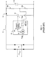
- Figure 1 illustrates the operation of an exemplary
analog PFC chip 20. The circuit receives applied sinusoidal AC voltage at the input of afull wave rectifier 10 and produces a full wave rectified sinusoidal voltage at the output of the rectifier. The full wave rectified sinusoidal voltage from the rectifier is applied to one terminal of afiltering inductor 12. Coupled to the other terminal of theinductor 12 is aswitching device 16 such as a power MOSFET or an IGBT. The other terminal of theswitching device 16 is coupled to the negative rail of the DC bus. APFC chip 20 provides switching signals to switch theswitching device 16 on and off. ThePFC chip 20 receives as input a full wave rectified sinusoidal voltage which is in phase with the sinusoidal voltage applied to therectifier 10. ThePFC chip 20 also receives a signal representing the desired voltage across the DC bus (VREF). ADC bus capacitor 18 is coupled across the positive and negative rails of the DC bus. Adiode 14 is provided to prevent current from flowing back to the line from the load. - In operation, the
PFC chip 20 opens and closesswitching device 16 so that the load across thefull wave rectifier 10 varies from the inductor 12 (whenswitch 16 is closed) to the inductor and the DC bus capacitor 18 (whenswitch 16 is opened). This is accomplished through the use of acurrent control circuit 26.Current control circuit 26 operates according to known techniques to switchswitching device 16. The current input command to the current control circuit is provided by ananalog multiplier 25 which multiplies the VSINE input (containing the phase information) with a signal from analog error amplifier 22 (which will also have compensation components, not shown, for stabilising the system) corresponding to the difference between the desired DC bus voltage (VREF) and a signal corresponding to the actual bus voltage. In Figure 1, the voltage corresponding to the actual bus voltage is taken from a voltagedivider comprising resistors switch 16 in a manner corresponding to the voltage variations in the sinusoidal input tofull wave rectifier 10, the power factor of the system may be improved. - One limitation of known PFC circuits, such as
chip 20 in Figure 1, is that they require analog circuitry, such asanalog error amplifier 22 andanalog multiplier 25. The manufacture of such analog circuits is relatively difficult and relatively expensive when compared to the manufacture of circuits employing digital circuits. It is an object of the present invention to overcome these and other problems in the prior art by providing a digital PFC chip that is easily implemented and provides cost and manufacturing advantages over known analog PFC chips. - The present invention is defined in the accompanying independent claims. Preferred features are recited in the dependent claims.
- In accordance with one aspect of the present invention, a power factor correction circuit for improving the power factor of an electric circuit including a DC bus is provided, where the electric circuit operates from an AC line voltage. In this embodiment, the power factor correction circuit includes a rectifier coupled to the AC line voltage for providing a rectified voltage signal; a switching device that, when closed, provides a current path from the positive output of the rectifier to the reference output of the rectifier via a filter inductor; a current sensor for sensing the current flowing through the switching device; a pulse width modulation controlled attenuator coupled to the output of the rectifier, wherein the pulse width modulation controlled attenuator provides an attenuated version of the rectified voltage signal that has a magnitude corresponding to a pulse width modulation control signal; and a current controller coupled to the current sensor and the variable attenuator for controlling the switching device such that the current flowing through the switching device follows an envelope which is substantially in phase with the attenuated version of the rectified voltage signal and has a magnitude proportional to the magnitude of the attenuated version of the rectified signal.
- A further embodiment of the present invention involves the use in a power factor correction circuit of a digital power factor correction chip, formed as a single integrated circuit, that includes a digital comparator for comparing a voltage corresponding to the desired DC bus voltage with a voltage corresponding to the actual DC bus voltage; an up/down counter having an up/down control input coupled to the output of the digital comparator and a clock input adapted to receive a fixed frequency clock signal; and a digital pulse width modulation generator coupled to receive the output of the up/down counter, for generating the pulse width modulation control signal, where the duty cycle of the pulse width modulation control signal corresponds to the output of the up/down counter. In this embodiment, the pulse width modulation control signal is used to control a pulse width modulation controlled attenuator that attenuates the rectified source voltage.
- Other aspects and advantages of the present invention will become apparent upon reading the following detailed description of some embodiments of the invention given by way of example with reference to the drawings in which:
- Figure 1 is a schematic diagram of a prior art analog PFC chip;
- Figure 2 is a schematic diagram of a digital PFC chip in accordance with the present invention; and
- Figure 3 is a schematic diagram of a further embodiment of a digital PFC chip in accordance with the present invention.
- Similar reference characters indicate similar parts throughout the several views of the drawings.
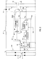
- Turning now to Figure 2, a
digital PFC circuit 30 in accordance with the present invention is illustrated. - In Figure 2, as in the circuit of Figure 1, a sinusoidal AC signal is applied to the input of a
full wave rectifier 10 which provides a full wave rectified sinusoidal signal at its output. Coupled to one output of therectifier 10 is aninductor 12.Inductor 12 is also coupled to the positive rail of the DC bus via adiode 14. As in Figure 1, a switching device 16' is connected across the output ofinductor 12 and the reference rail of the DC bus. APFC circuit 30 controls the switching of switching device 16' such that the power factor of the circuit is improved. - Unlike the circuit of Figure 1, the embodiment of the present invention illustrated in Figure 2 utilizes a
digital PFC chip 30 to control the switching of switching device 16'. The digital PFC chip receives a signal representative of the desired DC bus voltage (VREF) and through the use of digital circuitry controls the switching of switching device 16' to both provide the desired DC bus voltage and to improve the power factor of the circuit. - In general, the
digital PFC chip 30 uses a controlled digital attenuator to provide an attenuated voltage signal that is in phase with the applied AC line voltage and has a magnitude that varies in response to the difference between the desired DC bus voltage and the actual DC bus voltage. That attenuated voltage signal is then used as a current command for a current controller that controls the current drawn from the AC line. - Referring to Figure 2, the switching of switching device 16' is controlled to provide an improved power factor for the circuit by ensuring that the current drawn from the AC line is substantially in phase with the applied AC voltage and undistorted. In the circuit of Figure 2, this is accomplished though the use of a minimum off
timer 48,digital comparator 46 andcurrent feedback resistor 36. In a preferred embodiment, thedigital comparator 46 and minimum offtimer 48 are both located within thePFC chip 30. - As described more fully below, when
PFC chip 30 is operating, a sinusoidal voltage signal that is in phase with the AC voltage applied torectifier 10 is applied to theinput 40 ofdigital PFC chip 30. This sinusoidal voltage signal is compared with a current feedback signal indigital comparator 46. The current feedback signal corresponds to the current flowing throughresistor 36, and generally corresponds to the current that is drawn from the AC line by the circuit.Digital comparator 46 compares the current feedback signal with the sinusoidal voltage signal provided atinput 40 and, through minimum offtimer 48 controls the switching of switch 16'. - In the embodiment of Figure 2, when the current feedback signal is less than the voltage at
input 40, the output fromdigital comparator 46 will be a logic high and the switching device 16' will be switched ON, or closed. In this configuration, increasing current will flow from the output ofrectifier 10, through theinductor 12 and through the series circuit of switching device 16' andresistor 36. As the current flowing throughresistor 36 increases, a point will be reached where the current feedback signal exceeds the voltage oninput 40. When this occurs, the output ofdigital comparator 46 will change from logic high to logic low and the switching device 16' will be switched OFF and the current will be diverted throughdiode 14 and will be used to chargeDC bus capacitor 18. When switching device 16' is opened, the current flowing throughresistor 36 will drop to zero, and the output ofdigital comparator 46 changes back from logic low to logic high. After the time interval of minimum off/timer 48 has expired, which in a preferred embodiment is 10µ sec, switching device 16' will again be switched ON and the process will repeat. - As the above discussion indicates, minimum off-
timer 48,digital comparator 46 andcurrent feedback resistor 36 operate to draw an average current fromrectifier 10 that: (i) is in phase with the voltage applied to input 40; and (ii) has a magnitude that corresponds to the magnitude of the voltage applied atinput 40. - In Figure 2 the voltage applied to the
input 40 of thedigital PFC chip 30 is an attenuated version of the output of thefull wave rectifier 10 that is substantially in phase with the AC line voltage applied torectifier 10. As described below, the magnitude of the voltage applied to input 40 is controlled bydigital PFC chip 30 to maintain the DC bus voltage at a desired level. - In the embodiment of Figure 2, the full wave rectified sinusoidal voltage appearing at the output of the rectifier is divided down by a voltage
divider comprising resistors resistors input 40 of thedigital PFC chip 30 via aresistor 33. - Coupled to the junction of
resistors resistor 35, which is coupled to the negative rail of the DC bus by aswitching device 34.Switching device 34 may be an IGBT, a MOSFET, a power transistor or the like and preferably is contained within thePFC chip 30. When switchingdevice 34 is open, there is no current path from the junction ofresistors resistor 35 to ground. As such, when switchingdevice 34 is open, it is as if theresistor 35 is not present and the voltage appearing at theinput 40 ofdigital PFC chip 30 will be a reduced version of the full wave rectified sinusoidal voltage appearing at the output ofrectifier 10 where the instantaneous voltage applied to the input 40 (V40) is roughly the instantaneous voltage at the output of rectifier times R32b/(R32a + R32b), where R32a and R32b represent the resistances ofresistors device 34 is closed, there is a current path from the junction ofresistors resistor 35 to ground as if theresistor 35 is connected in parallel withresistor 32b. Thus, when switchingdevice 34 is closed, the voltage appearing at theinput 40 ofdigital PFC chip 30 will be a reduced version of the full wave rectified sinusoidal voltage VO appearing at the output ofrectifier 10 where the instantaneous voltage applied to the input 40 (V40) is roughly the instantaneous voltage at the output of rectifier times Rx/(R32a + Rx), where Rx is the value of theparallel resistors input 40 ofdigital PFC chip 30 will be a smaller fraction of the output ofrectifier 10 when switchingdevice 34 is closed than when it is open. - By controlling the percentage of time that switching
device 34 is closed (i.e., its "on time"), it is possible to control the magnitude of the voltage applied to input 40 of thedigital PFC chip 30 from a maximum of Vo ∗ R32b/(R32a + R32b), when the on-time duty cycle is 0%, to a minimum value of Vo ∗ Rx/(R32a + Rx) when the on-time duty cycle is 100%. In this manner, the resistivedivider comprising resistors - The relative values of
resistors rectifier 10. If the RMS AC input voltage is around 120V, then the peak value of Vo will be around 170V. Assuming that around 1W could be dissipated in the resistors, this would require the sum of R32a and R32b to be around 30kΩ. Suitable values for these two resistors would be 30kΩ and 500 Ω respectively. The value of R35 could then be chosen to be around 20% of R32b, i.e. around 100Ω. R33 is simply chosen according to normal practice to provide, in conjunction withcapacitor 38, a suitable filter time constant for the voltage V40 so that the ripple due to the switching action ofswitch 34 is suppressed. A value of 5kΩ would be appropriate. - In the embodiment of Figure 2, the PWM duty cycle of the
switching device 34 is controlled by a digital pulsewidth modulation generator 44, of conventional construction which is located on thePFC chip 30. As those skilled in the art will appreciate, a digital PWM generator receives as its input a digital word corresponding to a particular duty-cycle and produces a PWM signal of constant repetition rate that has the desired duty cycle. - In Figure 2, the digital word which forms the input to
digital PWM generator 44 is provided by an UP/DOWN counter 42. UP/DOWN counter 42, which is located on thePFC chip 30, receives as inputs an external clock signal (CLK) and an UP/DOWN control signal fromdigital comparator 41. - In operation,
digital comparator 41 compares a voltage signal representing the desired DC bus voltage with a signal corresponding to the actual DC bus voltage. In Figure 2, the signal corresponding to the DC bus voltage (VDC) is taken from a voltagedivider comprising resistors differential amplifier 22 from Figure 1,digital comparator 41 in Figure 2 does not provide an analog output that represents the difference between its inputs; it merely provides a digital output where, for example, a logic 1 indicates that VREF is greater than VDC, and a logic 0 indicates that VDC is greater than VREF. - The logic 1 or logic 0 output from
digital comparator 41 is applied to the UP/DOWN input ofcounter 42. As such,counter 42 will count UP as long as VREF is greater than VDC and will begin to count down when VDC exceeds VREF. Thus, in steady-state operation, when the DC bus voltage is near the desired DC bus voltage, thecounter 42 will provide at its output a digital word that hovers around a certain nominal value that corresponds to the desired DC bus voltage. - The digital word from
counter 42 is provided to thePWM generator 44 and is used to control the switching of switchingdevice 34 and thus the magnitude of the voltage applied to input 40. In the embodiment of Figure 2, the count corresponds to the off-time for the pulse width modulated control signal (i.e., the portion oftime switch 34 is open). Thus, a high count fromcounter 42 represents the situation where the reference voltage is much greater than the DC bus voltage and correspondingly theswitching device 34 will be switched such that the voltage applied to input 40 is at its maximum possible value. Progressively lower counts from counter 44 correspond to a progressively longer switching duty cycle of switchingdevice 34 such that the magnitude of the voltage applied to input 40 is reduced. - The
digital PFC chip 30 of Figure 2 controls the switching of switchingdevices 34 and 16' such that the desired DC bus voltage is maintained and the power factor of the circuit is improved. In particular, when the circuit is first operated, the magnitude of the DC bus voltage will be less than that of the desired DC bus voltage. As such,counter 44 will begin to count up, causing the magnitude of the input applied to input 40 to progressively increase. At some point, the magnitude of the DC bus voltage will reach and exceed the desired DC bus voltage, causing thecounter 42 to begin counting down and reducing the magnitude of the voltage applied to input 40. This will in turn cause a slight reduction in the DC bus voltage, which will cause counter 42 to begin counting up again. Eventually a steady-state condition will be reached where the output ofcounter 42 hovers around a certain value. - In addition to controlling the magnitude of the DC bus voltage, as described above, the
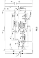
digital PFC chip 30 of Figure 2 also improves the power factor by switching device 16' such that the average current drawn from therectifier 10 is in phase with the voltage applied to input 40 which -- in Figure 2 -- is in phase with the voltage applied to the input ofrectifier 10. - The system shown in Figure 2 is a basic system which, while generally producing the required output, can suffer from sub-harmonic oscillation. This is because the controller feedback system only has an integral term. An alternate embodiment is shown in Figure 3.
- In Figure 3, the
comparator 41 of Figure 2 is replaced by an analog to digital converter (ADC) 51 and adigital multiplier 52 is added to the circuit. This changes the controller feedback system from integral only to proportional plus integral (P+I). - The analog to
digital converter 51 provides a digital representation of the DC bus voltage, in a manner familiar to those skilled in the art. This digital word is subtracted from a digital voltage demand reference indigital subtractor 60 to produce a bus voltage error (BVE). This is multiplied in thedigital multiplier circuit 52 with either a pre-programmed or an externally variable multiplication factor. This multiplier effectively adds a P gain term. The up/down counter 42 of Figure 2 continues to supply an I gain term, the P and I terms being added in adigital adder 62 before being supplied to the PWM generator. Theswitch 34 of Figure 2 can be replaced by abuffer 65, as shown in Figure 3. Those skilled in the art will recognize that the I gain term may also be pre-programmed or externally programmed. This embodiment results in the bus voltage being held stable and avoids any tendency for low-frequency oscillations to appear on the bus voltage. - The remainder of the circuitry of Figure 3 operates in a manner similar to the circuitry of Figure 2.
- The above description of several embodiments is made by way of example and not for purposes of limitation. The present invention is intended to be limited only by the spirit and scope of the following claims.
Claims (15)
- A power factor correction circuit for improving the power factor of an electric circuit including a DC bus, where the electric circuit operates from an alternating source, the power factor correction circuit comprising:a rectifier coupled to the alternating source for providing a rectified voltage;a switching device actuatable to provide a current path from a positive output of the rectifier to a reference output of the rectifier;a current sensor for sensing the current in the current path;a pulse width modulation controlled attenuator coupled to the output of the rectifier, wherein the pulse width modulation controlled attenuator provides an attenuated version of the rectified voltage that has a magnitude corresponding to a pulse width modulation control signal; anda current controller coupled to the current sensor and the variable attenuator for controlling the switching device such that the magnitude of the current flowing in the current path follows an envelope which is substantially in phase with the attenuated version of the rectified voltage signal and is related to the magnitude of the attenuated version of the rectified signal.
- A circuit as claimed in claim 1, further comprising an inductor coupled between the positive output of the rectifier and the switching device.
- A circuit as claimed in claim 1 or 2, wherein the pulse width modulation control signal is provided by a digital circuit comprising:a digital comparator for comparing a voltage corresponding to the desired DC bus voltage with a voltage corresponding to the actual DC bus voltage;an up/down counter having an up/down control input coupled to the output of the digital comparator and a clock input adapted to receive a fixed frequency clock signal; anda digital pulse width modulation generator coupled to receive the output of the up/down counter for generating the pulse width modulation control signal, where the duty cycle of the pulse width modulation control signal corresponds to the output of the up/down counter.
- A circuit as claimed in claim 3, wherein the pulse width modulation attenuator comprises:a voltage divider comprising a first resistor coupled to the positive output of the rectifier and a second resistor coupled to the first resistor and to the reference output of the rectifier;a third resistor electrically coupled to the junction of the first resistor and the second resistor;a further switching device that, when closed, provides a current path from the junction of the first and second resistors, through the third resistor, to the reference output of the rectifier, wherein the further switching device is controlled by the pulse width modulation control signal.
- A circuit as claimed in any of claims 1 to 4, wherein the current sensor comprises a sense resistor coupled between the switching device and the reference output of the rectifier.
- A circuit as claimed in claims 1 to 5, wherein the current controller comprises a digital comparator for comparing the output of the current sensor with the attenuated version of the rectified voltage and wherein the output of the digital comparator controls the switching of the switching device.
- A circuit as claimed in claim 6, further comprising a minimum off timer coupled between the digital comparator and the switching device.
- A circuit as claimed in claim 6, wherein the switching device is open when the output of the digital comparator is logic low, and wherein the output of the digital comparator is logic low when the voltage across the sense resistor is greater than the attenuated version of the rectified voltage.
- A circuit as claimed in claim 3, wherein the output of the digital comparator is logic high when the voltage corresponding to the desired DC bus voltage is greater than the voltage corresponding to the actual DC bus voltage.
- A circuit as claimed in claim 9, wherein the up/down counter counts up whenever the output of the digital comparator is logic high.
- A circuit as claimed in any of claims 1 to 10, wherein the pulse width modulation control signal is provided by a digital circuit comprising:an analog to digital converter for connecting a voltage representing the actual DC bus voltage to a digital value corresponding to the actual DC bus voltage;a digital subtractor for providing a digital value corresponding to the difference between the digital value corresponding to the desired DC bus voltage and a digital value representing the desired DC bus voltage;a digital pulse width modulation generator coupled to receive the output of the digital subtractor for generating the pulse width modulation control signal, where the duty cycle of the pulse width modulation control signal corresponds to the output of the digital subtractor.
- A circuit as claimed in claim 11, further including a further up/down counter responsive to the output of the digital subtractor wherein the duty cycle of the pulse width modulation control signal corresponds to the sum of the output of the further up/down counter and the output of the digital subtractor.
- A circuit as claimed in claim 11, wherein the pulse width modulation generator comprises a buffer coupled to receive the pulse width modulation control signal, a resistor coupled to the output of the buffer and to a voltage divider coupled across the output of the rectifier.
- A method of improving the power factor of an electric circuit that receives power from a time varying voltage source, the method comprising the steps of:comparing the actual DC bus voltage with a desired DC bus voltage and providing a digital signal indicating whether the desired DC bus voltage is greater than the actual DC bus voltage;increasing a count on a periodic basis whenever the desired DC bus voltage is greater than the actual DC bus voltage, and decreasing the count whenever the desired DC bus voltage is less than the actual DC bus voltage;generating a pulse width modulation signal having a duty cycle that corresponds to the count;attenuating the source voltage by an amount corresponding to the duty cycle of the pulse width modulation signal; andactuating a switching device coupled to the electric circuit to draw a current that is in phase with the attenuated source voltage and has a magnitude corresponding to the magnitude of the attenuated source voltage.
- The method of claim 21 further comprising the step of providing the source voltage by rectifying an AC line voltage.
Applications Claiming Priority (2)
| Application Number | Priority Date | Filing Date | Title |
|---|---|---|---|
| GB9608832 | 1996-04-30 | ||
| GBGB9608832.3A GB9608832D0 (en) | 1996-04-30 | 1996-04-30 | Power factor correction circuit |
Publications (3)
| Publication Number | Publication Date |
|---|---|
| EP0805548A2 true EP0805548A2 (en) | 1997-11-05 |
| EP0805548A3 EP0805548A3 (en) | 1999-02-24 |
| EP0805548B1 EP0805548B1 (en) | 2006-07-05 |
Family
ID=10792816
Family Applications (1)
| Application Number | Title | Priority Date | Filing Date |
|---|---|---|---|
| EP97300443A Expired - Lifetime EP0805548B1 (en) | 1996-04-30 | 1997-01-24 | Power factor correction circuit |
Country Status (6)
| Country | Link |
|---|---|
| US (1) | US5801935A (en) |
| EP (1) | EP0805548B1 (en) |
| KR (1) | KR100431782B1 (en) |
| DE (1) | DE69736260T2 (en) |
| GB (1) | GB9608832D0 (en) |
| TW (1) | TW368774B (en) |
Cited By (8)
| Publication number | Priority date | Publication date | Assignee | Title |
|---|---|---|---|---|
| EP0982845A3 (en) * | 1998-08-28 | 2000-05-24 | Switched Reluctance Drives Limited | Switched reluctance drive with high power factor |
| EP1104083A1 (en) * | 1999-11-24 | 2001-05-30 | Lucent Technologies Inc. | Power factor correcting electrical converter apparatus |
| EP0991169A3 (en) * | 1998-10-01 | 2002-01-23 | Osram Sylvania Inc. | Wave shaping circuit |
| WO2002019523A1 (en) * | 2000-08-30 | 2002-03-07 | Infineon Technologies Ag | Filter system and method for filtering an analog signal |
| EP1445852A2 (en) | 2003-02-07 | 2004-08-11 | Baumüller Nürnberg Gmbh | Device and method for active power factor correction |
| WO2007096263A1 (en) * | 2006-02-21 | 2007-08-30 | Osram Gesellschaft mit beschränkter Haftung | Step-up driver with minimal switching frequency |
| WO2011019723A2 (en) | 2009-08-10 | 2011-02-17 | Emerson Climate Technologies, Inc. | System and method for reducing line current distortion |
| EP2478998B1 (en) * | 2007-03-21 | 2018-01-10 | Mirka Oy | Control method for an electric sanding machine |
Families Citing this family (32)
| Publication number | Priority date | Publication date | Assignee | Title |
|---|---|---|---|---|
| US6138042A (en) * | 1997-12-31 | 2000-10-24 | Motorola, Inc. | Method, device, phone, and base station for providing an efficient tracking power converter for variable signals |
| JP3744680B2 (en) * | 1998-03-31 | 2006-02-15 | 富士通株式会社 | Power supply device and method for controlling power supply circuit |
| KR100286047B1 (en) * | 1998-05-15 | 2001-04-16 | 김덕중 | Power Factor Correction Circuit Using Inverse Sawtooth Wave |
| KR100303450B1 (en) * | 1998-05-29 | 2001-11-30 | 김덕중 | Pfc controller |
| US6128205A (en) * | 1999-05-07 | 2000-10-03 | Philips Electronics North America Corporation | Power factor correction with reduced total harmonic distortion |
| CN2402549Y (en) * | 1999-12-02 | 2000-10-25 | 杜顺兴 | Double-circuit car safety belt automatic warning device |
| DE10035418A1 (en) * | 2000-07-20 | 2002-02-14 | Infineon Technologies Ag | Fully digital voltage converter |
| US7201244B2 (en) * | 2003-10-03 | 2007-04-10 | Letourneau, Inc. | Vehicle for materials handling and other industrial uses |
| ITMI20032095A1 (en) * | 2003-10-28 | 2005-04-29 | Roal Electronics S P A | DEVICE FOR CONTROL OF THE POWER FACTOR. |
| US6967851B2 (en) * | 2003-12-15 | 2005-11-22 | System General Corp. | Apparatus for reducing the power consumption of a PFC-PWM power converter |
| KR100867452B1 (en) * | 2004-06-07 | 2008-11-10 | 인터내쇼널 렉티파이어 코포레이션 | Low switching frequency power factor correction circuit |
| JP2006042477A (en) * | 2004-07-26 | 2006-02-09 | Smk Corp | Wave shaping circuit |
| JP2006158067A (en) * | 2004-11-29 | 2006-06-15 | Renesas Technology Corp | Power supply driver circuit |
| US7359224B2 (en) * | 2005-04-28 | 2008-04-15 | International Rectifier Corporation | Digital implementation of power factor correction |
| US7208895B2 (en) | 2005-06-24 | 2007-04-24 | Emerson Electric Co. | Control systems and methods for permanent magnet rotating machines |
| US7342379B2 (en) | 2005-06-24 | 2008-03-11 | Emerson Electric Co. | Sensorless control systems and methods for permanent magnet rotating machines |
| US7323851B2 (en) * | 2005-09-22 | 2008-01-29 | Artesyn Technologies, Inc. | Digital power factor correction controller and AC-to-DC power supply including same |
| KR100790709B1 (en) * | 2006-10-25 | 2008-01-02 | 삼성전기주식회사 | Converter with waveform conversion of input current |
| TW200847593A (en) * | 2007-05-18 | 2008-12-01 | Richtek Techohnology Corp | Digital voltage transformer and its control method |
| US8358098B2 (en) * | 2009-08-10 | 2013-01-22 | Emerson Climate Technologies, Inc. | System and method for power factor correction |
| US8476873B2 (en) * | 2009-08-10 | 2013-07-02 | Emerson Climate Technologies, Inc. | System and method for current balancing |
| US8264860B2 (en) * | 2009-08-10 | 2012-09-11 | Emerson Climate Technologies, Inc. | System and method for power factor correction frequency tracking and reference generation |
| US8698433B2 (en) | 2009-08-10 | 2014-04-15 | Emerson Climate Technologies, Inc. | Controller and method for minimizing phase advance current |
| US8508166B2 (en) | 2009-08-10 | 2013-08-13 | Emerson Climate Technologies, Inc. | Power factor correction with variable bus voltage |
| US8344706B2 (en) * | 2009-08-10 | 2013-01-01 | Emerson Climate Technologies, Inc. | System and method for rejecting DC current in power factor correction systems |
| US8493014B2 (en) * | 2009-08-10 | 2013-07-23 | Emerson Climate Technologies, Inc. | Controller and method for estimating, managing, and diagnosing motor parameters |
| US8264192B2 (en) | 2009-08-10 | 2012-09-11 | Emerson Climate Technologies, Inc. | Controller and method for transitioning between control angles |
| CN103503296B (en) * | 2011-04-26 | 2016-06-01 | 瑞萨电子株式会社 | PFC signal generating circuit, the PFC Controlling System using PFC signal generating circuit and PFC control method |
| JP5584826B2 (en) | 2011-04-26 | 2014-09-03 | ルネサスエレクトロニクス株式会社 | PFC signal generation circuit, PFC control system using the same, and PFC control method |
| KR101296386B1 (en) * | 2012-02-21 | 2013-08-12 | 옵티멀파워디자인 주식회사 | Wide range operation pfc circuit |
| US9634593B2 (en) | 2012-04-26 | 2017-04-25 | Emerson Climate Technologies, Inc. | System and method for permanent magnet motor control |
| US9240749B2 (en) | 2012-08-10 | 2016-01-19 | Emerson Climate Technologies, Inc. | Motor drive control using pulse-width modulation pulse skipping |
Family Cites Families (11)
| Publication number | Priority date | Publication date | Assignee | Title |
|---|---|---|---|---|
| US4109194A (en) * | 1977-06-09 | 1978-08-22 | Bell Telephone Laboratories, Incorporated | Digital feedback control utilizing accumulated reference count to regulate voltage output of switching regulator |
| US4361792A (en) * | 1980-05-06 | 1982-11-30 | Chesebrough-Pond's Inc. | Digital induction motor control system |
| EP0059053A3 (en) * | 1981-02-21 | 1983-05-18 | THORN EMI plc | Switched mode power supply |
| US4459529A (en) * | 1981-04-20 | 1984-07-10 | Nordic Controls Co. | Power factor control circuit for AC motors |
| WO1984002404A1 (en) * | 1982-12-11 | 1984-06-21 | Fairford Electronics Ltd | Method and apparatus for automatically setting the demand phase lag input to an induction-motor power factor controller |
| US5151642A (en) * | 1990-05-03 | 1992-09-29 | Allen-Bradley Company, Inc. | Apparatus for controlling an electric motor |
| JP2610362B2 (en) * | 1990-07-27 | 1997-05-14 | 株式会社テック | High voltage power supply controller |
| US5481451A (en) * | 1992-10-30 | 1996-01-02 | Arex Electronics Corporation | AC-to-AC power inverter apparatus functioning without smoothing capacitor, and control method thereof |
| US5304911A (en) * | 1992-12-14 | 1994-04-19 | Energy Consortium Inc | Power control system for an A.C. induction motor |
| US5432693A (en) * | 1993-04-01 | 1995-07-11 | Ford Motor Company | Digital pulse width modulator circuit with proportional dither |
| US5656923A (en) * | 1995-04-10 | 1997-08-12 | The Whitaker Corporation | A DC power supply controller |
-
1996
- 1996-04-30 GB GBGB9608832.3A patent/GB9608832D0/en active Pending
- 1996-09-09 US US08/708,804 patent/US5801935A/en not_active Expired - Lifetime
-
1997
- 1997-01-24 DE DE69736260T patent/DE69736260T2/en not_active Expired - Fee Related
- 1997-01-24 EP EP97300443A patent/EP0805548B1/en not_active Expired - Lifetime
- 1997-03-04 TW TW086102549A patent/TW368774B/en active
- 1997-04-30 KR KR1019970016412A patent/KR100431782B1/en not_active Expired - Fee Related
Cited By (14)
| Publication number | Priority date | Publication date | Assignee | Title |
|---|---|---|---|---|
| EP0982845A3 (en) * | 1998-08-28 | 2000-05-24 | Switched Reluctance Drives Limited | Switched reluctance drive with high power factor |
| US6201368B1 (en) | 1998-08-28 | 2001-03-13 | Switched Reluctance Drives Limited | Switched reluctance drive with high power factor |
| EP0991169A3 (en) * | 1998-10-01 | 2002-01-23 | Osram Sylvania Inc. | Wave shaping circuit |
| EP1104083A1 (en) * | 1999-11-24 | 2001-05-30 | Lucent Technologies Inc. | Power factor correcting electrical converter apparatus |
| WO2002019523A1 (en) * | 2000-08-30 | 2002-03-07 | Infineon Technologies Ag | Filter system and method for filtering an analog signal |
| US6753798B2 (en) | 2000-08-30 | 2004-06-22 | Infineon Technologies Ag | Filter configuration, method for filtering an analog filter input signal, and power factor controller |
| EP1445852A2 (en) | 2003-02-07 | 2004-08-11 | Baumüller Nürnberg Gmbh | Device and method for active power factor correction |
| EP1445852A3 (en) * | 2003-02-07 | 2005-06-22 | Baumüller Nürnberg Gmbh | Device and method for active power factor correction |
| WO2007096263A1 (en) * | 2006-02-21 | 2007-08-30 | Osram Gesellschaft mit beschränkter Haftung | Step-up driver with minimal switching frequency |
| US8134301B2 (en) | 2006-02-21 | 2012-03-13 | Osram Ag | Step-up driver with minimal switching frequency |
| EP2478998B1 (en) * | 2007-03-21 | 2018-01-10 | Mirka Oy | Control method for an electric sanding machine |
| EP3385031A3 (en) * | 2007-03-21 | 2018-11-14 | Mirka Oy | Control method for an electric sanding machine |
| WO2011019723A2 (en) | 2009-08-10 | 2011-02-17 | Emerson Climate Technologies, Inc. | System and method for reducing line current distortion |
| EP2465190A4 (en) * | 2009-08-10 | 2018-03-21 | Emerson Climate Technologies, Inc. | System and method for reducing line current distortion |
Also Published As
| Publication number | Publication date |
|---|---|
| GB9608832D0 (en) | 1996-07-03 |
| EP0805548A3 (en) | 1999-02-24 |
| DE69736260D1 (en) | 2006-08-17 |
| TW368774B (en) | 1999-09-01 |
| US5801935A (en) | 1998-09-01 |
| DE69736260T2 (en) | 2007-05-31 |
| KR970072667A (en) | 1997-11-07 |
| KR100431782B1 (en) | 2004-08-25 |
| EP0805548B1 (en) | 2006-07-05 |
Similar Documents
| Publication | Publication Date | Title |
|---|---|---|
| EP0805548B1 (en) | Power factor correction circuit | |
| EP0779700B1 (en) | DC power supply with enhanced input power factor | |
| US8164930B2 (en) | Power factor correction circuit | |
| JP3994953B2 (en) | Power factor correction circuit | |
| US5001620A (en) | Power factor improvement | |
| US6049473A (en) | Harmonic-injection control technique for three-phase, discontinuous-conduction-mode, high-power-factor boost rectifiers with improved line-transient response | |
| KR100796890B1 (en) | Switching power supply | |
| JP6272691B2 (en) | Amplitude normalization circuit, power supply device and electronic device | |
| JPH0851790A (en) | Control circuit for inductive load | |
| JPH09205766A (en) | Power factor compensation circuit | |
| EP1580639B1 (en) | Transition mode power factor correction device in switching power supplies | |
| JP3565416B2 (en) | Power factor improvement circuit | |
| JP3484904B2 (en) | Power factor improvement circuit | |
| Bourgeois | Circuits for power factor correction with regards to mains filtering | |
| CN102577067A (en) | DC power supply device, and motor driving inverter apparatus using same | |
| WO2004107553A1 (en) | Inverter power source control circuit for high-frequency heater | |
| KR20200053925A (en) | Power transforming apparatus having noise reduction function, compressor including the same and the method for the same | |
| JP2001231262A (en) | DC motor control device | |
| JP2766805B2 (en) | Power supply smoothing device | |
| JPH04368471A (en) | Power source | |
| JPH02168864A (en) | Dc power supply device | |
| JP2001086737A (en) | Power supply | |
| JPH10127046A (en) | Control circuit for step-up converter | |
| JP2020156216A (en) | Power converter | |
| JPH03178563A (en) | Dc power supply |
Legal Events
| Date | Code | Title | Description |
|---|---|---|---|
| PUAI | Public reference made under article 153(3) epc to a published international application that has entered the european phase |
Free format text: ORIGINAL CODE: 0009012 |
|
| AK | Designated contracting states |
Kind code of ref document: A2 Designated state(s): DE ES FR GB IE IT NL SE |
|
| PUAL | Search report despatched |
Free format text: ORIGINAL CODE: 0009013 |
|
| AK | Designated contracting states |
Kind code of ref document: A3 Designated state(s): DE ES FR GB IE IT NL SE |
|
| 17P | Request for examination filed |
Effective date: 19990318 |
|
| 17Q | First examination report despatched |
Effective date: 20030115 |
|
| GRAP | Despatch of communication of intention to grant a patent |
Free format text: ORIGINAL CODE: EPIDOSNIGR1 |
|
| GRAS | Grant fee paid |
Free format text: ORIGINAL CODE: EPIDOSNIGR3 |
|
| GRAA | (expected) grant |
Free format text: ORIGINAL CODE: 0009210 |
|
| AK | Designated contracting states |
Kind code of ref document: B1 Designated state(s): DE ES FR GB IE IT NL SE |
|
| PG25 | Lapsed in a contracting state [announced via postgrant information from national office to epo] |
Ref country code: NL Free format text: LAPSE BECAUSE OF FAILURE TO SUBMIT A TRANSLATION OF THE DESCRIPTION OR TO PAY THE FEE WITHIN THE PRESCRIBED TIME-LIMIT Effective date: 20060705 Ref country code: IT Free format text: LAPSE BECAUSE OF FAILURE TO SUBMIT A TRANSLATION OF THE DESCRIPTION OR TO PAY THE FEE WITHIN THE PRE;WARNING: LAPSES OF ITALIAN PATENTS WITH EFFECTIVE DATE BEFORE 2007 MAY HAVE OCCURRED AT ANY TIME BEFORE 2007. THE CORRECT EFFECTIVE DATE MAY BE DIFFERENT FROM THE ONE RECORDED.SCRIBED TIME-LIMIT Effective date: 20060705 |
|
| REG | Reference to a national code |
Ref country code: GB Ref legal event code: FG4D |
|
| REG | Reference to a national code |
Ref country code: IE Ref legal event code: FG4D |
|
| REF | Corresponds to: |
Ref document number: 69736260 Country of ref document: DE Date of ref document: 20060817 Kind code of ref document: P |
|
| PG25 | Lapsed in a contracting state [announced via postgrant information from national office to epo] |
Ref country code: SE Free format text: LAPSE BECAUSE OF FAILURE TO SUBMIT A TRANSLATION OF THE DESCRIPTION OR TO PAY THE FEE WITHIN THE PRESCRIBED TIME-LIMIT Effective date: 20061005 |
|
| PG25 | Lapsed in a contracting state [announced via postgrant information from national office to epo] |
Ref country code: ES Free format text: LAPSE BECAUSE OF FAILURE TO SUBMIT A TRANSLATION OF THE DESCRIPTION OR TO PAY THE FEE WITHIN THE PRESCRIBED TIME-LIMIT Effective date: 20061016 |
|
| NLV1 | Nl: lapsed or annulled due to failure to fulfill the requirements of art. 29p and 29m of the patents act | ||
| PG25 | Lapsed in a contracting state [announced via postgrant information from national office to epo] |
Ref country code: IE Free format text: LAPSE BECAUSE OF NON-PAYMENT OF DUE FEES Effective date: 20070124 |
|
| PLBE | No opposition filed within time limit |
Free format text: ORIGINAL CODE: 0009261 |
|
| STAA | Information on the status of an ep patent application or granted ep patent |
Free format text: STATUS: NO OPPOSITION FILED WITHIN TIME LIMIT |
|
| 26N | No opposition filed |
Effective date: 20070410 |
|
| PG25 | Lapsed in a contracting state [announced via postgrant information from national office to epo] |
Ref country code: DE Free format text: LAPSE BECAUSE OF NON-PAYMENT OF DUE FEES Effective date: 20070801 |
|
| REG | Reference to a national code |
Ref country code: FR Ref legal event code: ST Effective date: 20070930 |
|
| PG25 | Lapsed in a contracting state [announced via postgrant information from national office to epo] |
Ref country code: FR Free format text: LAPSE BECAUSE OF NON-PAYMENT OF DUE FEES Effective date: 20070131 |
|
| PGFP | Annual fee paid to national office [announced via postgrant information from national office to epo] |
Ref country code: GB Payment date: 20160104 Year of fee payment: 20 |
|
| REG | Reference to a national code |
Ref country code: GB Ref legal event code: PE20 Expiry date: 20170123 |
|
| PG25 | Lapsed in a contracting state [announced via postgrant information from national office to epo] |
Ref country code: GB Free format text: LAPSE BECAUSE OF EXPIRATION OF PROTECTION Effective date: 20170123 |