EP0804059B1 - Structure for mounting an electrical module on a board - Google Patents
Structure for mounting an electrical module on a board Download PDFInfo
- Publication number
- EP0804059B1 EP0804059B1 EP97106749A EP97106749A EP0804059B1 EP 0804059 B1 EP0804059 B1 EP 0804059B1 EP 97106749 A EP97106749 A EP 97106749A EP 97106749 A EP97106749 A EP 97106749A EP 0804059 B1 EP0804059 B1 EP 0804059B1
- Authority
- EP
- European Patent Office
- Prior art keywords
- board
- daughter board
- lead frames
- daughter
- input
- Prior art date
- Legal status (The legal status is an assumption and is not a legal conclusion. Google has not performed a legal analysis and makes no representation as to the accuracy of the status listed.)
- Expired - Lifetime
Links
Images


Classifications
-
- H—ELECTRICITY
- H05—ELECTRIC TECHNIQUES NOT OTHERWISE PROVIDED FOR
- H05K—PRINTED CIRCUITS; CASINGS OR CONSTRUCTIONAL DETAILS OF ELECTRIC APPARATUS; MANUFACTURE OF ASSEMBLAGES OF ELECTRICAL COMPONENTS
- H05K3/00—Apparatus or processes for manufacturing printed circuits
- H05K3/36—Assembling printed circuits with other printed circuits
- H05K3/366—Assembling printed circuits with other printed circuits substantially perpendicularly to each other
-
- H—ELECTRICITY
- H01—ELECTRIC ELEMENTS
- H01R—ELECTRICALLY-CONDUCTIVE CONNECTIONS; STRUCTURAL ASSOCIATIONS OF A PLURALITY OF MUTUALLY-INSULATED ELECTRICAL CONNECTING ELEMENTS; COUPLING DEVICES; CURRENT COLLECTORS
- H01R12/00—Structural associations of a plurality of mutually-insulated electrical connecting elements, specially adapted for printed circuits, e.g. printed circuit boards [PCB], flat or ribbon cables, or like generally planar structures, e.g. terminal strips, terminal blocks; Coupling devices specially adapted for printed circuits, flat or ribbon cables, or like generally planar structures; Terminals specially adapted for contact with, or insertion into, printed circuits, flat or ribbon cables, or like generally planar structures
- H01R12/50—Fixed connections
- H01R12/51—Fixed connections for rigid printed circuits or like structures
- H01R12/52—Fixed connections for rigid printed circuits or like structures connecting to other rigid printed circuits or like structures
-
- H—ELECTRICITY
- H05—ELECTRIC TECHNIQUES NOT OTHERWISE PROVIDED FOR
- H05K—PRINTED CIRCUITS; CASINGS OR CONSTRUCTIONAL DETAILS OF ELECTRIC APPARATUS; MANUFACTURE OF ASSEMBLAGES OF ELECTRICAL COMPONENTS
- H05K2201/00—Indexing scheme relating to printed circuits covered by H05K1/00
- H05K2201/10—Details of components or other objects attached to or integrated in a printed circuit board
- H05K2201/10227—Other objects, e.g. metallic pieces
- H05K2201/10424—Frame holders
-
- H—ELECTRICITY
- H05—ELECTRIC TECHNIQUES NOT OTHERWISE PROVIDED FOR
- H05K—PRINTED CIRCUITS; CASINGS OR CONSTRUCTIONAL DETAILS OF ELECTRIC APPARATUS; MANUFACTURE OF ASSEMBLAGES OF ELECTRICAL COMPONENTS
- H05K2201/00—Indexing scheme relating to printed circuits covered by H05K1/00
- H05K2201/10—Details of components or other objects attached to or integrated in a printed circuit board
- H05K2201/10613—Details of electrical connections of non-printed components, e.g. special leads
- H05K2201/10742—Details of leads
- H05K2201/10886—Other details
- H05K2201/10946—Leads attached onto leadless component after manufacturing the component
-
- H—ELECTRICITY
- H05—ELECTRIC TECHNIQUES NOT OTHERWISE PROVIDED FOR
- H05K—PRINTED CIRCUITS; CASINGS OR CONSTRUCTIONAL DETAILS OF ELECTRIC APPARATUS; MANUFACTURE OF ASSEMBLAGES OF ELECTRICAL COMPONENTS
- H05K3/00—Apparatus or processes for manufacturing printed circuits
- H05K3/30—Assembling printed circuits with electric components, e.g. with resistors
- H05K3/32—Assembling printed circuits with electric components, e.g. with resistors electrically connecting electric components or wires to printed circuits
- H05K3/34—Assembling printed circuits with electric components, e.g. with resistors electrically connecting electric components or wires to printed circuits by soldering
- H05K3/3447—Lead-in-hole components
Definitions
- the present invention relates to a structure for mounting a module to a mother board tridimensionally by use of lead frames.
- DE-A-38 01 610 discloses a multiple connector for connecting printed circuit boards carrying electronic parts with wiring boards.
- An arc-shaped bridge is provided for connecting boards. One end of the bridge is secured to one of the boards and the other end is inserted into an opening in the respective other board.
- the bridge has a contact surface contacting the conductive surface of the wiring board. Additionally, one of the boards may have a guide pin to be inserted in the other board.
- FR-A-2 608 328 discloses with respect to a prior art embodiment a lead frame that is comb-shaped for nipping a daughter board at the pads . More precisely, the daughter board is received in the fork-type end portions of the respective lead frames, wherein the two outer fingers are arranged on one side of the board and the center finger is arranged on the opposite side of the board.
- EP-A-0 287 274 describes a device generally similar to the device of FR-A-2 608 328 mentioned above. More precisely, this document discloses that each of the leads is assigned to a respective terminal. This configuration makes it difficult to position the leads relative to a daughter-card and then connect the former to the latter.
- metal fittings 20 for connection each has a pair of flat body portions 21.
- Each body portion 21 has a number of parallel fingers 30 at its edge for gripping jumpers 35.
- a potbelley-like slit is formed in each finger 30 and open at its outer end.
- Lead terminals 22 extend out from each metal fitting while through holes 19 are formed in a mother printed circuit board or mother board 11.
- the lead terminals 22 are inserted in the through holes 19 and soldered to the mother board 11.
- a subprinted circuit board or daughter board 15 has its edge or card edge 16 inserted in aligned slits 23 formed in the metal fittings 20.
- the daughter board 15 is mounted to the mother board 11 in a vertical position.
- each jumper 35 has its opposite end portions pressed into the aligned fingers 30 of the nearby metal fittings 20. In this condition, the metal fittings 20 are interconnected by the jumper 35.
- the above arrangement of the jumpers 35 makes it needless to form a power supply pattern or similar broad pattern having a great current capacity on the mother board 11 or the daughter board 15; that is, the jumpers 35 play the role of such a broad pattern.
- FIG. 2 shows a module mounting structure and method disclosed in Japanese Patent Laid-Open Publication No. 1-304796 also mentioned earlier.
- an IC part 42 is mounted on the surface of a daughter board 41 by solder 43, constituting a module 44.
- a lead pin or lead frame 49 has a generally L-shaped section. The horizontal portion of the lead frame 49 is inserted in a through hole 41a formed in the daughter board 41 and affixed to the board 41 by solder 46. The vertical portion of the lead frame 49 is inserted in a through hole 47a formed in the mother board 47 and then affixed to the board 47 by solder 48.
- a first problem is that the structures cannot easily deal with the increasing number of pins of a daughter board.
- the metal fitting 20 taught in Laid-Open Publication No. 2-68982 has the slit 23 for nipping the edge of the daughter board 15, and the lead terminals 22 to be inserted in the through holes 19 of the mother board 11. Therefore, to accommodate a great number of pins, one metal fitting 20 must be assigned to each input/output terminal, resulting in complicated production.
- the lead frame taught in Laid-Open Publication No. 1-304796 has its one end press fitted in the through hole 41a of the daughter board 41. In this configuration, the lead frame 49 can be press fitted from only one side of the daughter board 41. Therefore, to accommodate a great number of pins, the diameter and pitch of the through holes 41a must be reduced, or the size of the daughter board 41 must be increased, resulting in low yield.
- a second problem is that the conventional structures are not adaptive to dense module mounting. Specifically, the metal fitting 20 prevents the daughter boards 15 to be mounted to the mother board 11 at a small pitch because the the size of the metal fitting 20 limits the mounting pitch.
- a third problem is that the conventional structures are not adaptive to high speed operation.
- the metal fitting 20 taught in Laid-Open Publication No. 2-68982 has a great surface area, and therefore a great capacitive load.
- a mother board 1 carries a number of electronic parts, not shown, thereon.
- a plurality of patterns, not shown, to be connected to a daughter board 3 are led out via the mother board 1, and each terminates at a respective through hole 2.
- Solder cream is printed on pads provided on the front and rear of the daughter board 3, and then a preselected electronic part 4 is mounted to the pads via the solder cream.
- a plurality of signal patterns, ground patterns and power supply patterns are led out at the end of the daughter board 3 adjoining the mother board 1 on each of the front and rear of the board 3.
- Input/output pads 7 each is provided on the end of the respective pattern.
- a plurality of lead frames 5 are affixed to an affixing member 6 and then respectively soldered to the input/output pads 7 at one end 5a thereof.
- the affixing member 6 is formed of resin.
- FIGS. 5A-5D show a specific configuration of the lead frames 5 and a specific configuration of the affixing block formed of resin 6.
- the lead frames 5 each having the configuration shown in FIGS. 5A and 5B are affixed to the affixing block 6, as shown in FIGS. 5C and 5D.
- the number of the lead frames 5 is the same as the number of the input/output pads 7 provided on one side of the daughter board 3. Lugs 9 protrude from both ends of the lower portion of the affixing block 6, as illustrated.
- the electronic parts 4 are mounted on the daughter board 3, as shown in FIG. 4 in detail.
- Reference holes 8 (see FIG. 6) are formed in the daughter board 3 at both ends of the lower portion of the board 3.
- the lugs 9 of the affixing block 6 are respectively received in the reference holes 8 in order to prevent the block 6 from being displaced relative to the daughter board 3.
- the lead frames 5 are affixed to the respective affixing block 6 on each side of the daughter board 3, and soldered to the input/output pads 7. Such two arrays of lead frames 5 are respectively inserted in two arrays of through holes 2 formed in the mother board 1. Subsequently, the lead frames 5 are soldered to the mother board 1, as shown in FIG. 4.
- the lead frames 5 are 5.955 mm long, 0.2 mm wide, and 0.1 mm thick each.
- the lead frames 5 are formed of phosphor bronze, and each is provided with a 1 ⁇ m thick Ni plating and a 2 ⁇ m thick solder plating overlying the Ni plating. Phosphor bronze may be replaced with brass, if desired.
- the daughter board 3 is implemented as a printed circuit board using glass epoxy resin or similar organic insulating resin although it may be implemented as a glass ceramic board.
- the resin constituting the affixing block 6 use is made of a liquid crystal polymer although it may be replaced with polyphenyl sulfide or similar heat-resistant resin.
- the present invention provides a module mounting structure having various unprecedented advantages, as follows. Input/output terminals for different kinds of signals can be provided on both sides of a daughter board, implementing dense module mounting.
- the structure is therefore adaptive to an increase in the number of pins without increasing the size of a daughter board. Because daughter boards are inserted in through holes formed in a mother board and then soldered to the mother board, there can be reduced the pitch of the daughter boards.
- daughter boards and a mother board are interconnected by the shortest distance, so that the structure of the present invention can deal with high speed operation.
- the interconnection distance is short enough to make an inductance component and a capacitance component negligibly small.
- modules like other parts, can be collectively mounted to a mother board by solder reflow, and because the daughter board can be inserted in through holes and affixed by soldering together with other DIP (Dual In-Line Package) parts.
- DIP Dual In-Line Package
Landscapes
- Engineering & Computer Science (AREA)
- Manufacturing & Machinery (AREA)
- Microelectronics & Electronic Packaging (AREA)
- Combinations Of Printed Boards (AREA)
- Multi-Conductor Connections (AREA)
- Coupling Device And Connection With Printed Circuit (AREA)
Description
- The present invention relates to a structure for mounting a module to a mother board tridimensionally by use of lead frames.
- To meet the increasing demand for a miniature, dense and high-speed electronic apparatus, it is a common practice to mount electronic parts and ICs (Integrated Circuits) to a printed circuit board to constitute a module, and to mount a number of such modules to a single mother board tridimensionally. The prerequisite with this kind of scheme is that the modules and mother board be electrically interconnected, mechanically surely supported, and low cost. Japanese Patent Laid-Open Publication No. 1-304796, for example, discloses a module mounting method of this kind. Japanese Patent Laid-Open Publication No. 2-68982 teaches a structure for mounting a printed circuit board. However, the conventional structures cannot deal with an increase in the number of pins of the daughter board or an increase in the density or operation speed of the module.
- DE-A-38 01 610 discloses a multiple connector for connecting printed circuit boards carrying electronic parts with wiring boards. An arc-shaped bridge is provided for connecting boards. One end of the bridge is secured to one of the boards and the other end is inserted into an opening in the respective other board. The bridge has a contact surface contacting the conductive surface of the wiring board. Additionally, one of the boards may have a guide pin to be inserted in the other board.
- FR-A-2 608 328 discloses with respect to a prior art embodiment a lead frame that is comb-shaped for nipping a daughter board at the pads . More precisely, the daughter board is received in the fork-type end portions of the respective lead frames, wherein the two outer fingers are arranged on one side of the board and the center finger is arranged on the opposite side of the board.
- EP-A-0 287 274 describes a device generally similar to the device of FR-A-2 608 328 mentioned above. More precisely, this document discloses that each of the leads is assigned to a respective terminal. This configuration makes it difficult to position the leads relative to a daughter-card and then connect the former to the latter.
- It is therefore an object of the present invention to provide a module mounting structure adaptive to an increase in the number of pins of a daughter board and an increase in operation speed. This object is achieved with the features of the claims.
- The above and other objects, features and advantages of the present invention will become apparent from the following detailed description taken with the accompanying drawings in which:
- FIG. 1A is a perspective view showing a conventional mounting structure;
- FIG. 1B is a fragmentary enlarged perspective view of the structure shown in FIG. 1A;
- FIG. 2 is a section showing another conventional mounting structure;
- FIG. 3 is a perspective view showing a mounting structure embodying the present invention;
- FIG. 4 is a section along line A-A of FIG. 3;
- FIG. 5A shows a specific configuration of a lead frame and a specific configuration of an affixing member both of which are included in the embodiment;
- FIG. 5B is a side elevation of the lead frame shown in FIG. 5A;
- FIG. 5C is a front view showing a plurality of lead frames affixed to the affixing member;
- FIG. 5D is a side elevation showing the lead frames and affixing block;
- FIG. 6 is a front view of a daughter board included in the embodiment; and
- FIG. 7 is a perspective view showing how the daughter board is mounted to a mother board in the illustrative embodiment.
-
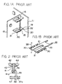
- To better understand the present invention, brief reference will be made to a conventional structure for mounting printed circuit boards, shown in FIGS. 1A and 1B. The structure to be described is taught in Japanese Patent Laid-Open Publication No. 2-68982 mentioned earlier. As shown,
metal fittings 20 for connection each has a pair offlat body portions 21. Eachbody portion 21 has a number ofparallel fingers 30 at its edge forgripping jumpers 35. A potbelley-like slit is formed in eachfinger 30 and open at its outer end. When thejumper 35 is inserted in the slit of any one of thefingers 30, thefinger 30 grips the periphery of thejumper 35, as illustrated.Notches 31 are formed in the portions of thefingers 30 adjoining thebody portion 21, so that needless ones of thefingers 30 can be easily bent and removed by hand. -
Lead terminals 22 extend out from each metal fitting while throughholes 19 are formed in a mother printed circuit board or mother board 11. Thelead terminals 22 are inserted in the throughholes 19 and soldered to the mother board 11. After themetal fittings 20 have been mounted to the mother board 11 in a vertical array, a subprinted circuit board ordaughter board 15 has its edge orcard edge 16 inserted in alignedslits 23 formed in themetal fittings 20. As a result, thedaughter board 15 is mounted to the mother board 11 in a vertical position. Subsequently, eachjumper 35 has its opposite end portions pressed into the alignedfingers 30 of thenearby metal fittings 20. In this condition, themetal fittings 20 are interconnected by thejumper 35. - The above arrangement of the
jumpers 35 makes it needless to form a power supply pattern or similar broad pattern having a great current capacity on the mother board 11 or thedaughter board 15; that is, thejumpers 35 play the role of such a broad pattern. - FIG. 2 shows a module mounting structure and method disclosed in Japanese Patent Laid-Open Publication No. 1-304796 also mentioned earlier. As shown, an
IC part 42 is mounted on the surface of adaughter board 41 bysolder 43, constituting amodule 44. A lead pin orlead frame 49 has a generally L-shaped section. The horizontal portion of thelead frame 49 is inserted in a through hole 41a formed in thedaughter board 41 and affixed to theboard 41 bysolder 46. The vertical portion of thelead frame 49 is inserted in athrough hole 47a formed in themother board 47 and then affixed to theboard 47 bysolder 48. - The conventional structures described above each has some problems left unsolved, as follows. A first problem is that the structures cannot easily deal with the increasing number of pins of a daughter board. Specifically, the
metal fitting 20 taught in Laid-Open Publication No. 2-68982 has theslit 23 for nipping the edge of thedaughter board 15, and thelead terminals 22 to be inserted in the throughholes 19 of the mother board 11. Therefore, to accommodate a great number of pins, onemetal fitting 20 must be assigned to each input/output terminal, resulting in complicated production. The lead frame taught in Laid-Open Publication No. 1-304796 has its one end press fitted in the through hole 41a of thedaughter board 41. In this configuration, thelead frame 49 can be press fitted from only one side of thedaughter board 41. Therefore, to accommodate a great number of pins, the diameter and pitch of the through holes 41a must be reduced, or the size of thedaughter board 41 must be increased, resulting in low yield. - A second problem is that the conventional structures are not adaptive to dense module mounting. Specifically, the
metal fitting 20 prevents thedaughter boards 15 to be mounted to the mother board 11 at a small pitch because the the size of the metal fitting 20 limits the mounting pitch. - A third problem is that the conventional structures are not adaptive to high speed operation. For example, the metal fitting 20 taught in Laid-Open Publication No. 2-68982 has a great surface area, and therefore a great capacitive load.
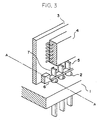
- Reference will be made to FIGS. 3 and 4 for describing a preferred embodiment of the module mounting structure in accordance with the present invention. As shown, a mother board 1 carries a number of electronic parts, not shown, thereon. A plurality of patterns, not shown, to be connected to a
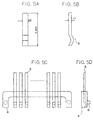
daughter board 3 are led out via the mother board 1, and each terminates at a respective throughhole 2. Solder cream is printed on pads provided on the front and rear of thedaughter board 3, and then a preselected electronic part 4 is mounted to the pads via the solder cream. A plurality of signal patterns, ground patterns and power supply patterns are led out at the end of thedaughter board 3 adjoining the mother board 1 on each of the front and rear of theboard 3. Input/output pads 7 each is provided on the end of the respective pattern. On each of the front and rear of thedaughter board 3, a plurality oflead frames 5 are affixed to an affixingmember 6 and then respectively soldered to the input/output pads 7 at oneend 5a thereof. The affixingmember 6 is formed of resin. - FIGS. 5A-5D show a specific configuration of the lead frames 5 and a specific configuration of the affixing block formed of
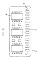
resin 6. The lead frames 5 each having the configuration shown in FIGS. 5A and 5B are affixed to the affixingblock 6, as shown in FIGS. 5C and 5D. The number of the lead frames 5 is the same as the number of the input/output pads 7 provided on one side of thedaughter board 3.Lugs 9 protrude from both ends of the lower portion of the affixingblock 6, as illustrated. The electronic parts 4 are mounted on thedaughter board 3, as shown in FIG. 4 in detail. Reference holes 8 (see FIG. 6) are formed in thedaughter board 3 at both ends of the lower portion of theboard 3. Thelugs 9 of the affixingblock 6 are respectively received in the reference holes 8 in order to prevent theblock 6 from being displaced relative to thedaughter board 3. - As shown in FIG. 7, the lead frames 5 are affixed to the
respective affixing block 6 on each side of thedaughter board 3, and soldered to the input/output pads 7. Such two arrays oflead frames 5 are respectively inserted in two arrays of throughholes 2 formed in the mother board 1. Subsequently, the lead frames 5 are soldered to the mother board 1, as shown in FIG. 4. - As shown in FIGS. 5A and 5B, the lead frames 5 are 5.955 mm long, 0.2 mm wide, and 0.1 mm thick each. The lead frames 5 are formed of phosphor bronze, and each is provided with a 1 µm thick Ni plating and a 2 µm thick solder plating overlying the Ni plating. Phosphor bronze may be replaced with brass, if desired. In the illustrative embodiment, the
daughter board 3 is implemented as a printed circuit board using glass epoxy resin or similar organic insulating resin although it may be implemented as a glass ceramic board. In the embodiment, for the resin constituting the affixingblock 6, use is made of a liquid crystal polymer although it may be replaced with polyphenyl sulfide or similar heat-resistant resin. - In summary, it will be seen that the present invention provides a module mounting structure having various unprecedented advantages, as follows. Input/output terminals for different kinds of signals can be provided on both sides of a daughter board, implementing dense module mounting. The structure is therefore adaptive to an increase in the number of pins without increasing the size of a daughter board. Because daughter boards are inserted in through holes formed in a mother board and then soldered to the mother board, there can be reduced the pitch of the daughter boards.
- Further, daughter boards and a mother board are interconnected by the shortest distance, so that the structure of the present invention can deal with high speed operation. Specifically, the interconnection distance is short enough to make an inductance component and a capacitance component negligibly small.
- Moreover, the structure is practicable with a conventional solder process and is therefore low cost. This is because modules, like other parts, can be collectively mounted to a mother board by solder reflow, and because the daughter board can be inserted in through holes and affixed by soldering together with other DIP (Dual In-Line Package) parts.
Claims (6)
- A module mounting structure comprising:a) a daughter board (3) carrying electronic parts (4) on both sides thereof, said daughter board (3) being provided with a plurality of input/output pads (7) on at least one side thereof;b) an affixing member (6) for affixing a plurality of substantially straight lead frames (5), each of said lead frames (5) having one end thereof soldered to a corresponding one of said plurality of input/output pads (7); andc) a mother board (1) formed with a plurality of through holes (2) respectively corresponding to said plurality of input/output pads (7), wherein the other end of each of said lead frames (5) is inserted in and soldered to a corresponding one of said plurality of through holes (2).
- The structure of claim 1, wherein a plurality of lead frames (5) is also soldered to said plurality of input/output pads (7) on the other side of said daughter board (3).
- The structure of claim 1 or 2, wherein said daughter board (3) comprises a printed circuit board using an organic resin as an insulating material.
- The structure of any of claims 1 to 3, wherein said daughter board (3) comprises a glass ceramic board.
- The structure of any of claims 1 to 4, wherein said affixing member (6) is formed of a liquid crystal polymer.
- The structure of any of claims 1 to 5, wherein said affixing member (6) is formed of a heat resistant resin.
Applications Claiming Priority (3)
| Application Number | Priority Date | Filing Date | Title |
|---|---|---|---|
| JP8101077A JPH09289052A (en) | 1996-04-23 | 1996-04-23 | Packaged structure of module |
| JP101077/96 | 1996-04-23 | ||
| JP10107796 | 1996-04-23 |
Related Child Applications (1)
| Application Number | Title | Priority Date | Filing Date |
|---|---|---|---|
| EP02002002 Division | 2002-02-05 |
Publications (2)
| Publication Number | Publication Date |
|---|---|
| EP0804059A1 EP0804059A1 (en) | 1997-10-29 |
| EP0804059B1 true EP0804059B1 (en) | 2004-08-11 |
Family
ID=14291046
Family Applications (1)
| Application Number | Title | Priority Date | Filing Date |
|---|---|---|---|
| EP97106749A Expired - Lifetime EP0804059B1 (en) | 1996-04-23 | 1997-04-23 | Structure for mounting an electrical module on a board |
Country Status (4)
| Country | Link |
|---|---|
| US (1) | US5796592A (en) |
| EP (1) | EP0804059B1 (en) |
| JP (1) | JPH09289052A (en) |
| DE (1) | DE69730174T2 (en) |
Families Citing this family (14)
| Publication number | Priority date | Publication date | Assignee | Title |
|---|---|---|---|---|
| US6020660A (en) * | 1997-12-10 | 2000-02-01 | General Electric Company | Dynamoelectric machine |
| US6335861B1 (en) | 1999-03-01 | 2002-01-01 | Cardiocommand, Inc. | Instrument platform using modular components |
| US20020192623A1 (en) * | 2001-06-15 | 2002-12-19 | Brad Sather | Method and apparatus for delivering educational training and assessment via the internet |
| US6893271B2 (en) * | 2003-10-08 | 2005-05-17 | Ingersoll-Rand Company | Circuit board assembly, main and connector boards, and connector pins for same |
| JP2005259962A (en) * | 2004-03-11 | 2005-09-22 | Fuji Electric Fa Components & Systems Co Ltd | Rectifier circuit mounting structure |
| TWI305130B (en) * | 2006-09-21 | 2009-01-01 | Delta Electronics Inc | Module supporting device |
| TWM327059U (en) * | 2007-03-16 | 2008-02-11 | Portwell Inc | Micro power supply |
| TWI403231B (en) * | 2008-03-11 | 2013-07-21 | Delta Electronics Inc | Surface-mounted circuit board module and fabrication method thereof |
| US20100254109A1 (en) * | 2009-03-19 | 2010-10-07 | Olympus Corporation | Mount assembly and method for manufacturing mount assembly |
| US9299674B2 (en) | 2012-04-18 | 2016-03-29 | Taiwan Semiconductor Manufacturing Company, Ltd. | Bump-on-trace interconnect |
| US9111817B2 (en) | 2012-09-18 | 2015-08-18 | Taiwan Semiconductor Manufacturing Company, Ltd. | Bump structure and method of forming same |
| US10109941B1 (en) * | 2017-06-30 | 2018-10-23 | Intel Corporation | Stepped slot connector to enable low height platforms |
| KR200490842Y1 (en) * | 2017-09-11 | 2020-01-13 | 삼어스코 주식회사 | Interface strucrure of surge protector |
| JP7505257B2 (en) * | 2020-05-18 | 2024-06-25 | 富士電機株式会社 | Substrate fixing structure, power unit and power conversion device |
Family Cites Families (12)
| Publication number | Priority date | Publication date | Assignee | Title |
|---|---|---|---|---|
| US3790916A (en) * | 1972-08-03 | 1974-02-05 | Gte Automatic Electric Lab Inc | Edge mount connector terminal |
| GB2103435A (en) * | 1981-06-17 | 1983-02-16 | British Insulated Callenders | Electrical connector for printed circuit boards |
| DE3138281C2 (en) * | 1981-09-25 | 1985-02-14 | Siemens AG, 1000 Berlin und 8000 München | Method for producing and attaching the pins of a carrier plate that can be plugged vertically onto a printed circuit board by means of several rows of these pins |
| JPS6377284U (en) * | 1986-11-10 | 1988-05-23 | ||
| FR2608328A1 (en) * | 1986-12-10 | 1988-06-17 | Ducellier & Cie | Method for connecting a first printed circuit to a second printed circuit, and printed circuits which enable such a method to be implemented and which are interconnected in this way |
| GB2203591A (en) * | 1987-04-14 | 1988-10-19 | Plessey Co Plc | Semiconductor hybrid device |
| DE3801610A1 (en) * | 1988-01-21 | 1989-08-03 | Diehl Gmbh & Co | Multiple connector |
| JPH01304796A (en) * | 1988-06-02 | 1989-12-08 | Fujitsu Ltd | Method for mounting module |
| JPH0268982A (en) * | 1988-09-02 | 1990-03-08 | Fujitsu Ltd | Mounting structure of printed board |
| FI91204C (en) * | 1991-03-19 | 1994-05-25 | Nokia Mobile Phones Ltd | Method for interconnecting circuit boards at an electrical apparatus and a connection obtained by method |
| DE4113335C1 (en) * | 1991-04-24 | 1992-11-05 | Dr. Johannes Heidenhain Gmbh, 8225 Traunreut, De | |
| DE4445658C2 (en) * | 1994-04-15 | 1997-10-23 | Phoenix Contact Gmbh & Co | Method for equipping a base strip of a connector for a printed circuit board with contact connections |
-
1996
- 1996-04-23 JP JP8101077A patent/JPH09289052A/en active Pending
-
1997
- 1997-04-21 US US08/844,659 patent/US5796592A/en not_active Expired - Lifetime
- 1997-04-23 DE DE69730174T patent/DE69730174T2/en not_active Expired - Fee Related
- 1997-04-23 EP EP97106749A patent/EP0804059B1/en not_active Expired - Lifetime
Also Published As
| Publication number | Publication date |
|---|---|
| DE69730174D1 (en) | 2004-09-16 |
| DE69730174T2 (en) | 2004-12-30 |
| EP0804059A1 (en) | 1997-10-29 |
| US5796592A (en) | 1998-08-18 |
| JPH09289052A (en) | 1997-11-04 |
Similar Documents
| Publication | Publication Date | Title |
|---|---|---|
| US6862190B2 (en) | Adapter for plastic-leaded chip carrier (PLCC) and other surface mount technology (SMT) chip carriers | |
| US5562462A (en) | Reduced crosstalk and shielded adapter for mounting an integrated chip package on a circuit board like member | |
| US5786989A (en) | Printed circuit board mounting structure and electronic device using the same | |
| EP0804059B1 (en) | Structure for mounting an electrical module on a board | |
| JP2559954B2 (en) | Stepped multi-layer interconnection device | |
| EP1035759A2 (en) | Edge-mountable integrated circuit package and method of attaching the same to a printed wiring board | |
| US20010041465A1 (en) | Z-axis electrical interconnect | |
| US4835345A (en) | Printed wiring board having robber pads for excess solder | |
| KR19990029586A (en) | Surface Mount Flexible Splicer | |
| WO1997002631A1 (en) | Electrical connectors | |
| US6271480B1 (en) | Electronic device | |
| US5444299A (en) | Electronic package with lead wire connections | |
| US5772450A (en) | Electrical connectors having external circuit connections | |
| RU240123U1 (en) | Adapter for installing TSSOP-10 packaged chips on the back side of a DIP-10 footprint on the main printed circuit board | |
| RU240504U1 (en) | Adapter for installing microcircuits in SSOP-10 package on the back side of DIP-10 mounting site on the main printed circuit board | |
| RU240515U1 (en) | An adapter board for installing TSSOP-12 packaged microcircuits from the back of a DIP-12 footprint on the main printed circuit board. | |
| RU240763U1 (en) | An adapter board for installing SSOP-12 packaged microcircuits from the back of a DIP-12 footprint on the main printed circuit board. | |
| RU240505U1 (en) | Adapter for installing microcircuits in the SO-10 package on the back side of the DIP-10 seat on the main printed circuit board | |
| US6950315B2 (en) | High frequency module mounting structure in which solder is prevented from peeling | |
| RU240758U1 (en) | An adapter board for installing microcircuits in an SO-8 package from the back of a DIP-8 footprint on the main printed circuit board. | |
| RU240766U1 (en) | An adapter board for installing microcircuits in a SOP-8 package from the back side of a DIP-8 footprint on the main printed circuit board. | |
| RU240496U1 (en) | Adapter for installing microcircuits in SOP-10 package on the back side of DIP-10 mounting site on the main printed circuit board | |
| RU240180U1 (en) | An adapter board for installing microcircuits in the MSOP-10 package from the back side of the DIP-10 footprint on the main printed circuit board | |
| RU240498U1 (en) | Adapter for installing microcircuits in SOIC-10 package on the back side of DIP-10 seat on the main printed circuit board | |
| RU240301U1 (en) | An adapter board for installing microcircuits in the SSOP-10 package from the back side of the DIP-10 footprint on the main printed circuit board. |
Legal Events
| Date | Code | Title | Description |
|---|---|---|---|
| PUAI | Public reference made under article 153(3) epc to a published international application that has entered the european phase |
Free format text: ORIGINAL CODE: 0009012 |
|
| 17P | Request for examination filed |
Effective date: 19970806 |
|
| AK | Designated contracting states |
Kind code of ref document: A1 Designated state(s): DE FR NL |
|
| 17Q | First examination report despatched |
Effective date: 19980518 |
|
| APAB | Appeal dossier modified |
Free format text: ORIGINAL CODE: EPIDOS NOAPE |
|
| APAB | Appeal dossier modified |
Free format text: ORIGINAL CODE: EPIDOS NOAPE |
|
| APAD | Appeal reference recorded |
Free format text: ORIGINAL CODE: EPIDOS REFNE |
|
| APAB | Appeal dossier modified |
Free format text: ORIGINAL CODE: EPIDOS NOAPE |
|
| GRAH | Despatch of communication of intention to grant a patent |
Free format text: ORIGINAL CODE: EPIDOS IGRA |
|
| GRAS | Grant fee paid |
Free format text: ORIGINAL CODE: EPIDOSNIGR3 |
|
| GRAA | (expected) grant |
Free format text: ORIGINAL CODE: 0009210 |
|
| AK | Designated contracting states |
Kind code of ref document: B1 Designated state(s): DE FR NL |
|
| RIC1 | Information provided on ipc code assigned before grant |
Ipc: 7H 01R 12/20 B Ipc: 7H 01R 12/18 B Ipc: 7H 05K 1/14 B Ipc: 7H 05K 3/36 A |
|
| REF | Corresponds to: |
Ref document number: 69730174 Country of ref document: DE Date of ref document: 20040916 Kind code of ref document: P |
|
| ET | Fr: translation filed | ||
| PLBE | No opposition filed within time limit |
Free format text: ORIGINAL CODE: 0009261 |
|
| STAA | Information on the status of an ep patent application or granted ep patent |
Free format text: STATUS: NO OPPOSITION FILED WITHIN TIME LIMIT |
|
| 26N | No opposition filed |
Effective date: 20050512 |
|
| APAH | Appeal reference modified |
Free format text: ORIGINAL CODE: EPIDOSCREFNO |
|
| PGFP | Annual fee paid to national office [announced via postgrant information from national office to epo] |
Ref country code: FR Payment date: 20080312 Year of fee payment: 12 Ref country code: DE Payment date: 20080502 Year of fee payment: 12 |
|
| PGFP | Annual fee paid to national office [announced via postgrant information from national office to epo] |
Ref country code: NL Payment date: 20080415 Year of fee payment: 12 |
|
| NLV4 | Nl: lapsed or anulled due to non-payment of the annual fee |
Effective date: 20091101 |
|
| REG | Reference to a national code |
Ref country code: FR Ref legal event code: ST Effective date: 20091231 |
|
| PG25 | Lapsed in a contracting state [announced via postgrant information from national office to epo] |
Ref country code: DE Free format text: LAPSE BECAUSE OF NON-PAYMENT OF DUE FEES Effective date: 20091103 |
|
| PG25 | Lapsed in a contracting state [announced via postgrant information from national office to epo] |
Ref country code: NL Free format text: LAPSE BECAUSE OF NON-PAYMENT OF DUE FEES Effective date: 20091101 |
|
| PG25 | Lapsed in a contracting state [announced via postgrant information from national office to epo] |
Ref country code: FR Free format text: LAPSE BECAUSE OF NON-PAYMENT OF DUE FEES Effective date: 20091222 |