EP0803983A2 - Superconducting input interface circuit for superconducting circuit - Google Patents
Superconducting input interface circuit for superconducting circuit Download PDFInfo
- Publication number
- EP0803983A2 EP0803983A2 EP97111509A EP97111509A EP0803983A2 EP 0803983 A2 EP0803983 A2 EP 0803983A2 EP 97111509 A EP97111509 A EP 97111509A EP 97111509 A EP97111509 A EP 97111509A EP 0803983 A2 EP0803983 A2 EP 0803983A2
- Authority
- EP
- European Patent Office
- Prior art keywords
- superconducting
- circuit
- signal
- field effect
- effect device
- Prior art date
- Legal status (The legal status is an assumption and is not a legal conclusion. Google has not performed a legal analysis and makes no representation as to the accuracy of the status listed.)
- Withdrawn
Links
- 230000005669 field effect Effects 0.000 claims abstract description 18
- 230000008878 coupling Effects 0.000 claims abstract description 7
- 238000010168 coupling process Methods 0.000 claims abstract description 7
- 238000005859 coupling reaction Methods 0.000 claims abstract description 7
- 239000002887 superconductor Substances 0.000 description 10
- IJGRMHOSHXDMSA-UHFFFAOYSA-N Atomic nitrogen Chemical compound N#N IJGRMHOSHXDMSA-UHFFFAOYSA-N 0.000 description 6
- 239000000463 material Substances 0.000 description 6
- 239000007788 liquid Substances 0.000 description 4
- 238000010586 diagram Methods 0.000 description 3
- 229910052757 nitrogen Inorganic materials 0.000 description 3
- 239000004065 semiconductor Substances 0.000 description 3
- 230000008054 signal transmission Effects 0.000 description 3
- 150000001875 compounds Chemical class 0.000 description 2
- 238000001816 cooling Methods 0.000 description 2
- 230000005672 electromagnetic field Effects 0.000 description 2
- 229910015901 Bi-Sr-Ca-Cu-O Inorganic materials 0.000 description 1
- QPLDLSVMHZLSFG-UHFFFAOYSA-N Copper oxide Chemical class [Cu]=O QPLDLSVMHZLSFG-UHFFFAOYSA-N 0.000 description 1
- 229910002480 Cu-O Inorganic materials 0.000 description 1
- 230000005540 biological transmission Effects 0.000 description 1
- 239000003990 capacitor Substances 0.000 description 1
- 230000007547 defect Effects 0.000 description 1
- 230000007613 environmental effect Effects 0.000 description 1
- 239000001307 helium Substances 0.000 description 1
- 229910052734 helium Inorganic materials 0.000 description 1
- SWQJXJOGLNCZEY-UHFFFAOYSA-N helium atom Chemical compound [He] SWQJXJOGLNCZEY-UHFFFAOYSA-N 0.000 description 1
- 239000012212 insulator Substances 0.000 description 1
- 230000010354 integration Effects 0.000 description 1
- 238000012986 modification Methods 0.000 description 1
- 230000004048 modification Effects 0.000 description 1
- 238000012856 packing Methods 0.000 description 1
Images
Classifications
-
- H—ELECTRICITY
- H03—ELECTRONIC CIRCUITRY
- H03K—PULSE TECHNIQUE
- H03K19/00—Logic circuits, i.e. having at least two inputs acting on one output; Inverting circuits
- H03K19/02—Logic circuits, i.e. having at least two inputs acting on one output; Inverting circuits using specified components
- H03K19/195—Logic circuits, i.e. having at least two inputs acting on one output; Inverting circuits using specified components using superconductive devices
-
- H—ELECTRICITY
- H03—ELECTRONIC CIRCUITRY
- H03F—AMPLIFIERS
- H03F19/00—Amplifiers using superconductivity effects
-
- Y—GENERAL TAGGING OF NEW TECHNOLOGICAL DEVELOPMENTS; GENERAL TAGGING OF CROSS-SECTIONAL TECHNOLOGIES SPANNING OVER SEVERAL SECTIONS OF THE IPC; TECHNICAL SUBJECTS COVERED BY FORMER USPC CROSS-REFERENCE ART COLLECTIONS [XRACs] AND DIGESTS
- Y10—TECHNICAL SUBJECTS COVERED BY FORMER USPC
- Y10S—TECHNICAL SUBJECTS COVERED BY FORMER USPC CROSS-REFERENCE ART COLLECTIONS [XRACs] AND DIGESTS
- Y10S505/00—Superconductor technology: apparatus, material, process
- Y10S505/70—High TC, above 30 k, superconducting device, article, or structured stock
- Y10S505/701—Coated or thin film device, i.e. active or passive
Definitions
- the present invention relates to a superconducting input interface circuit for a superconducting circuit, and more specifically to a superconducting interface circuit which transforms a signal sent by an ordinary electronic circuit to a suitable signal for a superconducting circuit.
- superconducting devices utilized in a conventional electronic equipment are limited to a switching device and a sensor device including a Josephson junction, a resister, a capacitor and an inductor. Therefore, a complicated circuit still can not be composed of only the superconducting devices alone. Moreover, the superconducting circuit has a small voltage swing range less than millivolts. By this, a weak signal of a few millivolts or a few microvolts are transferred through the superconducting circuit.
- the signal in order to transmit a signal of several volts from an ordinary electronic circuit to the superconducting circuit, the signal should be converted to have a voltage swing of a few millivolts or a few microvolts by a normal conducting interface circuit, and then this small voltage swing signal is sent to the superconducting circuit cooled by liquid nitrogen or liquid helium.
- This small voltage swing signal sent to the superconducting circuit from the interface circuit is easily affected and disturbed by external electromagnetic waves. Therefore, multiplexing and coding of the small voltage swing signal are restricted so as to decrease the possibility of introducing an error from these processing.
- This restriction of the multiplexing and coding of the small voltage swing signal leads to an increase of the number of signal lines.
- the above mentioned superconducting circuit has a small voltage/current gain, it has insufficient drivability. In order to compensate for the drivability of the superconducting circuit, the number of the signal lines further increases.
- the stable transmission of the small voltage swing signal also requires a complete electromagnetic shield around the signal lines.
- the electromagnetic shield needs additional space.
- Another object of the present invention is to provide a superconducting interface circuit which transfrom a signal sent by a normal circuit to a suitable signal for a superconducting circuit.
- a superconducting interface circuit converting a signal sent from a normal conducting circuit into a small voltage swing signal suitable for the normal conducting circuit into a small voltage swing signal suitable for the superconducting circuit, comprising two superconducting field effect devices, characterized in that the superconducting gate electrode of the first superconducting field effect device is connected to a signal line which transmits a voltage signal from the normal conducting circuit, the superconducting drain of this first superconducting field effect device is connected to a ground line, and the superconducting source of the first superconducting field effect device is connected to the superconducting drain and the gate electrode of the second superconducting field effect device; and the superconducting source of the second superconducting field effect device is connected to a power line; and in that the superconducting interface circuit is connected to the superconducting circuit through a magnetic coupling.
- the superconducting interface circuit in accordance with the present invention can directly receive a signal of several volts sent by an ordinary electronic circuit, for example a CMOS circuit. Therefore, by using the superconducting interface circuit in accordance with the present invention, the signal transmission from the ordinary electronic circuit section to the superconducting section becomes stable and is hard to be affected by an environmental electromagnetic field. In addition, multiplexing and coding of the signals become much easier.
- the number of signal lines between the ordinary electronic circuit section and the superconducting section can be reduced and an electromagnetic shield for the signal lines can be omitted so that a high packing arrangement becomes possible.
- the super-FET utilized in the superconducting interface circuit has a superconducting channel of an extremely thin oxide superconductor.
- Superconducting current flowing through the superconducting channel is controlled by a signal voltage of several volts applied to a gate electrode arranged on the superconducting channel through a gate insulator.
- the gate can be closed by a voltage of 5 volts and superconducting current is completely shut off. Therefore, a signal voltage of 5 or 3.3 volts from a CMOS device can be directly sent to the gate electrode of the super-FET and can directly drive the super-FET.
- superconducting current of 10 mA can flow through the superconducting channel having a width of 100 ⁇ m.
- the superconducting channel, superconducting source region and superconducting drain region of the above super-FET are formed of for example Y 1 Ba 2 Cu 3 O 7- ⁇ oxide superconductor material.
- these superconducting regions are preferably formed of not only Y 1 Ba 2 Cu 3 O 7- ⁇ oxide superconductor material but also a high-T c (high critical temperature) oxide superconductor material, particularly a high-T c copper-oxide type compound oxide superconductor material, for example a Bi-Sr-Ca-Cu-O compound oxide superconductor material, and a Tl-Ba-Ca-Cu-O compound oxide superconductor material.
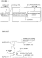
- FIG. 1 shows an embodiment of an electronic equipment including the superconducting interface circuit in accordance with the present invention.
- the electronic equipment includes an ordinary semiconductor circuit 4 and a superconducting section 5 which are connected to each other by a signal line 6.
- the superconducting section 5 includes a superconducting interface circuit 1 in accordance with the present invention and a superconducting circuit 2 utilizing an oxide superconductor which are connected by a magnetic coupling utilizing a solenoid 14.
- the entire superconducting section 5 is cooled by liquid nitrogen.
- the ordinary circuit 4 includes an output circuit 3 utilizing a CMOS semiconductor device, which are connected to the superconducting interface circuit 1 by the signal line 6, precisely.
- a signal transmission along the signal line 6 has an output voltage level of 5.0 vots or 3.3 volts, which is produced by the CMOS semiconductor device of the output circuit 3.
- This ordinary voltage level signal is difficult to be disturbed by external electromagnetic fields.
- the signal is converted to a small voltage swing signal which is suitable for the superconducting circuit 2 by the superconducting interface circuit and is sent to the superconducting circuit 2 through the magnetic coupling utilizing the solenoid 14. Therefore, in the electronic equipment including the superconducting interface circuit 1 in accordance with the present invention, the small voltage swing signal is transmitted only in the superconducting section 5. Since it is easy to form a magnetic shield which covers the entire superconducting section 5 and this magnetic shield does not need so large space, stable signal transmission from the ordinary circuit 4 to the superconducting section 5 and high density integration becomes possible in the electronic equipment.
- FIG. 2 shows a wiring diagram of an embodiment of the superconducting interface circuit which is used in the electronic equipment shown in Figure 1.
- the superconducting interface circuit includes two super-FETs 11, 12.
- the first super-FET has a superconducting gate connected to the signal line 6, a superconducting drain connected to the ground line 16 and a superconducting source connected to the superconducting drain and the superconducting gate of the second super-FET 12.
- the second super-FET 12 has a superconducting source connected to a power line 15.
- the superconducting interface circuit 1 is magnetically coupled to the superconducting circuit 2 by the solenoid 14, which is positioned near the super-FET 11.
- the super-FETs 11 and 12 have a large superconducting current capability and the flow of the superconducting current is controlled by a signal voltage of several voltages applied to their gates. Therefore, the signal transmitted along the signal line 6 of 5.0 volts or 3.3 volts can be converted to a small voltage swing signal suitable for the superconducting circuit 2 by this superconducting interface circuit.
- the super-FET has a large current capability and current driving ability so that it can send superconducting signals to plural superconducting circuits through a magnetic coupling.
- superconducting current flowing through the superconducting channel of the super-FET is controlled by a signal voltage of several volts applied to the gate electrode. Therefore, the signal can be directly sent from a CMOS device to the gate electrode of the super-FET.
- the superconducting interface circuit in accordance with the present invention it becomes unnecessary to convert a signal into a small voltage swing signal suitable for a superconducting circuit before the signal is sent from a normal conducting circuit, so that the signal sent from the normal conducting circuit has an ordinary level. This makes it easy to send a multiplexed and coded signal from a normal conducting circuit to a superconducting circuit.
Landscapes
- Engineering & Computer Science (AREA)
- Physics & Mathematics (AREA)
- Computer Hardware Design (AREA)
- Computing Systems (AREA)
- General Engineering & Computer Science (AREA)
- Mathematical Physics (AREA)
- Power Engineering (AREA)
- Superconductor Devices And Manufacturing Methods Thereof (AREA)
- Logic Circuits (AREA)
Abstract
Description
- The present invention relates to a superconducting input interface circuit for a superconducting circuit, and more specifically to a superconducting interface circuit which transforms a signal sent by an ordinary electronic circuit to a suitable signal for a superconducting circuit.
- When a superconducting device or a superconducting integrated circuit is adopted to an electronic equipment, it needs to be associated with a conventional electronic circuit operating at an ordinary temperature. Since it is still impossible for the superconducting device or the superconducting integrated circuit to complete the entire electronic equipment.
- Owing to the real nature of superconducting phenomena, such as problems of cooling etc., superconducting devices utilized in a conventional electronic equipment are limited to a switching device and a sensor device including a Josephson junction, a resister, a capacitor and an inductor. Therefore, a complicated circuit still can not be composed of only the superconducting devices alone. Moreover, the superconducting circuit has a small voltage swing range less than millivolts. By this, a weak signal of a few millivolts or a few microvolts are transferred through the superconducting circuit.
- In the prior art, in order to transmit a signal of several volts from an ordinary electronic circuit to the superconducting circuit, the signal should be converted to have a voltage swing of a few millivolts or a few microvolts by a normal conducting interface circuit, and then this small voltage swing signal is sent to the superconducting circuit cooled by liquid nitrogen or liquid helium.
- This small voltage swing signal sent to the superconducting circuit from the interface circuit is easily affected and disturbed by external electromagnetic waves. Therefore, multiplexing and coding of the small voltage swing signal are restricted so as to decrease the possibility of introducing an error from these processing. This restriction of the multiplexing and coding of the small voltage swing signal leads to an increase of the number of signal lines. In addition, since the above mentioned superconducting circuit has a small voltage/current gain, it has insufficient drivability. In order to compensate for the drivability of the superconducting circuit, the number of the signal lines further increases.
- The stable transmission of the small voltage swing signal also requires a complete electromagnetic shield around the signal lines. The electromagnetic shield needs additional space.
- The increase of the number of the signal lines and the attachment of the electromagnetic shield bring difficulties for realizing a highly integrated superconducting circuit.
- Accordingly, it is an object of the present invention to provide an input interface circuit for a superconducting circuit which has overcome the above mentioned defect of the conventional one.
- Another object of the present invention is to provide a superconducting interface circuit which transfrom a signal sent by a normal circuit to a suitable signal for a superconducting circuit.
- The above and other objects of the present invention are achieved in accordance with the present invention by a superconducting interface circuit converting a signal sent from a normal conducting circuit into a small voltage swing signal suitable for the normal conducting circuit into a small voltage swing signal suitable for the superconducting circuit, comprising two superconducting field effect devices, characterized in that the superconducting gate electrode of the first superconducting field effect device is connected to a signal line which transmits a voltage signal from the normal conducting circuit, the superconducting drain of this first superconducting field effect device is connected to a ground line, and the superconducting source of the first superconducting field effect device is connected to the superconducting drain and the gate electrode of the second superconducting field effect device; and the superconducting source of the second superconducting field effect device is connected to a power line; and in that the superconducting interface circuit is connected to the superconducting circuit through a magnetic coupling.
- The superconducting interface circuit in accordance with the present invention can directly receive a signal of several volts sent by an ordinary electronic circuit, for example a CMOS circuit. Therefore, by using the superconducting interface circuit in accordance with the present invention, the signal transmission from the ordinary electronic circuit section to the superconducting section becomes stable and is hard to be affected by an environmental electromagnetic field. In addition, multiplexing and coding of the signals become much easier.
- By all of these, the number of signal lines between the ordinary electronic circuit section and the superconducting section can be reduced and an electromagnetic shield for the signal lines can be omitted so that a high packing arrangement becomes possible.
- The super-FET utilized in the superconducting interface circuit has a superconducting channel of an extremely thin oxide superconductor. Superconducting current flowing through the superconducting channel is controlled by a signal voltage of several volts applied to a gate electrode arranged on the superconducting channel through a gate insulator. For example, if the superconducting channel of an oxide superconductor has a thickness of 5 nanometers, the gate can be closed by a voltage of 5 volts and superconducting current is completely shut off. Therefore, a signal voltage of 5 or 3.3 volts from a CMOS device can be directly sent to the gate electrode of the super-FET and can directly drive the super-FET. In addition, superconducting current of 10 mA can flow through the superconducting channel having a width of 100µm.
- This large current capability of the super-FET makes it possible that plural superconducting circuit is connected to the superconducting interface circuit through a magnetic coupling.
- It is preferable that the superconducting channel, superconducting source region and superconducting drain region of the above super-FET are formed of for example Y1Ba2Cu3O7-δ oxide superconductor material. In this connection, these superconducting regions are preferably formed of not only Y1Ba2Cu3O7-δ oxide superconductor material but also a high-Tc (high critical temperature) oxide superconductor material, particularly a high-Tc copper-oxide type compound oxide superconductor material, for example a Bi-Sr-Ca-Cu-O compound oxide superconductor material, and a Tl-Ba-Ca-Cu-O compound oxide superconductor material. By using one of these oxide superconductor, a super-FET even operating under liquid nitrogen cooling can be realized.
- The above and other objects, features and advantages of the present invention will be apparent from the following description of preferred embodiments of the invention with reference to the accompanying drawings.
- Figure 1 is a block diagram of an embodiment of the electronic equipment including the superconducting interface circuit in accordance with the present invention;
- Figure 2 is a schematic wiring diagram of another embodiment of the superconducting interface circuit in accordance with the present invention used in the electronic equipment shown in Figure 1.
- Figure 1 shows an embodiment of an electronic equipment including the superconducting interface circuit in accordance with the present invention. The electronic equipment includes an
ordinary semiconductor circuit 4 and asuperconducting section 5 which are connected to each other by asignal line 6. Thesuperconducting section 5 includes asuperconducting interface circuit 1 in accordance with the present invention and asuperconducting circuit 2 utilizing an oxide superconductor which are connected by a magnetic coupling utilizing asolenoid 14. The entiresuperconducting section 5 is cooled by liquid nitrogen. - The
ordinary circuit 4 includes anoutput circuit 3 utilizing a CMOS semiconductor device, which are connected to thesuperconducting interface circuit 1 by thesignal line 6, precisely. A signal transmission along thesignal line 6 has an output voltage level of 5.0 vots or 3.3 volts, which is produced by the CMOS semiconductor device of theoutput circuit 3. This ordinary voltage level signal is difficult to be disturbed by external electromagnetic fields. The signal is converted to a small voltage swing signal which is suitable for thesuperconducting circuit 2 by the superconducting interface circuit and is sent to thesuperconducting circuit 2 through the magnetic coupling utilizing thesolenoid 14. Therefore, in the electronic equipment including thesuperconducting interface circuit 1 in accordance with the present invention, the small voltage swing signal is transmitted only in thesuperconducting section 5. Since it is easy to form a magnetic shield which covers theentire superconducting section 5 and this magnetic shield does not need so large space, stable signal transmission from theordinary circuit 4 to thesuperconducting section 5 and high density integration becomes possible in the electronic equipment. - Figure 2 shows a wiring diagram of an embodiment of the superconducting interface circuit which is used in the electronic equipment shown in Figure 1. The superconducting interface circuit includes two super-FETs 11, 12. The first super-FET has a superconducting gate connected to the
signal line 6, a superconducting drain connected to theground line 16 and a superconducting source connected to the superconducting drain and the superconducting gate of the second super-FET 12. The second super-FET 12 has a superconducting source connected to apower line 15. As explained above, thesuperconducting interface circuit 1 is magnetically coupled to thesuperconducting circuit 2 by thesolenoid 14, which is positioned near the super-FET 11. - As explained in detail hereinafter, the super-FETs 11 and 12 have a large superconducting current capability and the flow of the superconducting current is controlled by a signal voltage of several voltages applied to their gates. Therefore, the signal transmitted along the
signal line 6 of 5.0 volts or 3.3 volts can be converted to a small voltage swing signal suitable for thesuperconducting circuit 2 by this superconducting interface circuit. - The super-FET has a large current capability and current driving ability so that it can send superconducting signals to plural superconducting circuits through a magnetic coupling.
- As mentioned above, superconducting current flowing through the superconducting channel of the super-FET is controlled by a signal voltage of several volts applied to the gate electrode. Therefore, the signal can be directly sent from a CMOS device to the gate electrode of the super-FET. By using the superconducting interface circuit in accordance with the present invention, it becomes unnecessary to convert a signal into a small voltage swing signal suitable for a superconducting circuit before the signal is sent from a normal conducting circuit, so that the signal sent from the normal conducting circuit has an ordinary level. This makes it easy to send a multiplexed and coded signal from a normal conducting circuit to a superconducting circuit.
- The invention has thus been shown and described with reference to the specific embodiments. However, it should be noted that the present invention is in no way limited to the details of the illustrated structures but changes and modifications may be made within the scope of the appended claim.
Claims (1)
- A superconducting interface circuit (1) converting a signal sent from a normal conducting circuit (4) into a small voltage swing signal suitable for a superconducting circuit (2), comprising two superconducting field effect devices (11, 12), characterized in that the superconducting gate electrode of the first superconducting field effect device is connected to a signal line (6) which transmits a voltage signal from the normal conducting circuit (4), the superconducting drain of this first superconducting field effect device (11) is connected to a ground line (16), and the superconducting source of the first superconducting field effect device is connected to the superconducting drain and the gate electrode of the second superconducting field effect device (12); and the superconducting source of the second superconducting field effect device (12) is connected to a power line (15); and in that the superconducting interface circuit (1) is connected to the superconducting circuit (2) through a magnetic coupling.
Applications Claiming Priority (3)
| Application Number | Priority Date | Filing Date | Title |
|---|---|---|---|
| JP4136016A JP2822773B2 (en) | 1992-04-28 | 1992-04-28 | Superconducting interface circuit |
| JP136016/92 | 1992-04-28 | ||
| EP93401108A EP0568455B1 (en) | 1992-04-28 | 1993-04-28 | Superconducting input interface circuit for superconducting circuit |
Related Parent Applications (2)
| Application Number | Title | Priority Date | Filing Date |
|---|---|---|---|
| EP93401108A Division EP0568455B1 (en) | 1992-04-28 | 1993-04-28 | Superconducting input interface circuit for superconducting circuit |
| EP93401108.1 Division | 1993-04-28 |
Publications (2)
| Publication Number | Publication Date |
|---|---|
| EP0803983A2 true EP0803983A2 (en) | 1997-10-29 |
| EP0803983A3 EP0803983A3 (en) | 1998-04-15 |
Family
ID=15165218
Family Applications (2)
| Application Number | Title | Priority Date | Filing Date |
|---|---|---|---|
| EP93401108A Expired - Lifetime EP0568455B1 (en) | 1992-04-28 | 1993-04-28 | Superconducting input interface circuit for superconducting circuit |
| EP97111509A Withdrawn EP0803983A3 (en) | 1992-04-28 | 1993-04-28 | Superconducting input interface circuit for superconducting circuit |
Family Applications Before (1)
| Application Number | Title | Priority Date | Filing Date |
|---|---|---|---|
| EP93401108A Expired - Lifetime EP0568455B1 (en) | 1992-04-28 | 1993-04-28 | Superconducting input interface circuit for superconducting circuit |
Country Status (5)
| Country | Link |
|---|---|
| US (1) | US5345115A (en) |
| EP (2) | EP0568455B1 (en) |
| JP (1) | JP2822773B2 (en) |
| CA (1) | CA2094983C (en) |
| DE (1) | DE69319274T2 (en) |
Families Citing this family (4)
| Publication number | Priority date | Publication date | Assignee | Title |
|---|---|---|---|---|
| DE69218348T2 (en) * | 1991-11-30 | 1997-10-16 | Sumitomo Electric Industries | Superconducting device with extremely thin superconducting channel and manufacturing process |
| CA2943489C (en) | 2014-03-21 | 2019-11-12 | Google Inc. | Chip including classical and quantum computing processers |
| DE102024107622A1 (en) * | 2024-03-18 | 2025-09-18 | Physikalisch-Technische Bundesanstalt Braunschweig Und Berlin | Device for measuring at least one electrical property of an electrical arrangement and a method for calibrating such a device |
| US20260045940A1 (en) * | 2024-04-22 | 2026-02-12 | Northrop Grumman Systems Corporation | Superconducting data input system |
Family Cites Families (11)
| Publication number | Priority date | Publication date | Assignee | Title |
|---|---|---|---|---|
| US4360898A (en) * | 1980-06-30 | 1982-11-23 | International Business Machines Corporation | Programmable logic array system incorporating Josephson devices |
| JPS63308974A (en) * | 1987-06-11 | 1988-12-16 | Toshiba Corp | Superconducting transistor |
| JPH02391A (en) * | 1987-11-04 | 1990-01-05 | Sumitomo Electric Ind Ltd | superconducting field effect transistor |
| EP0344925B1 (en) * | 1988-06-02 | 1994-08-03 | Texas Instruments Incorporated | Superconductively loaded semiconductor logic device |
| US5010304A (en) * | 1989-11-03 | 1991-04-23 | General Electric Company | Cryogenically-cooled radio-frequency power amplifier |
| DE69030247D1 (en) * | 1990-02-01 | 1997-04-24 | Ibm | Semiconductor superconductor integrated circuit technology |
| JPH0834320B2 (en) * | 1990-02-02 | 1996-03-29 | 株式会社日立製作所 | Superconducting element |
| US5024993A (en) * | 1990-05-02 | 1991-06-18 | Microelectronics & Computer Technology Corporation | Superconducting-semiconducting circuits, devices and systems |
| FR2666175B1 (en) * | 1990-08-21 | 1992-10-16 | Thomson Csf | SUPERCONDUCTING FIELD EFFECT TRANSISTOR. |
| CA2052970C (en) * | 1990-10-08 | 1996-07-02 | Takao Nakamura | Superconducting device having an extremely thin superconducting channel formed of oxide superconductor material and method for manufacturing the same |
| EP0523275B1 (en) * | 1991-07-19 | 1996-02-28 | International Business Machines Corporation | Enhanced superconducting field-effect transistor with inverted MISFET structure and method for making the same |
-
1992
- 1992-04-28 JP JP4136016A patent/JP2822773B2/en not_active Expired - Lifetime
-
1993
- 1993-04-27 CA CA002094983A patent/CA2094983C/en not_active Expired - Fee Related
- 1993-04-28 EP EP93401108A patent/EP0568455B1/en not_active Expired - Lifetime
- 1993-04-28 US US08/053,207 patent/US5345115A/en not_active Expired - Fee Related
- 1993-04-28 DE DE69319274T patent/DE69319274T2/en not_active Expired - Fee Related
- 1993-04-28 EP EP97111509A patent/EP0803983A3/en not_active Withdrawn
Also Published As
| Publication number | Publication date |
|---|---|
| DE69319274T2 (en) | 1999-02-18 |
| EP0803983A3 (en) | 1998-04-15 |
| US5345115A (en) | 1994-09-06 |
| EP0568455A1 (en) | 1993-11-03 |
| EP0568455B1 (en) | 1998-06-24 |
| JP2822773B2 (en) | 1998-11-11 |
| CA2094983A1 (en) | 1993-10-29 |
| JPH05304322A (en) | 1993-11-16 |
| CA2094983C (en) | 1996-04-16 |
| DE69319274D1 (en) | 1998-07-30 |
Similar Documents
| Publication | Publication Date | Title |
|---|---|---|
| CA1315015C (en) | Field-effect device with a superconducting channel | |
| US5455519A (en) | Josephson logic circuit | |
| SE512591C2 (en) | Digital information device and method | |
| KR880009452A (en) | Superconducting devices | |
| CA2049433A1 (en) | Elongate superconductor elements comprising oxide superconductors, superconducting coils and methods of making such elements | |
| EP0803983A2 (en) | Superconducting input interface circuit for superconducting circuit | |
| US4710651A (en) | Josephson-junction logic device | |
| EP0292436A3 (en) | High current conductors and high field magnets using anisotropic superconductors | |
| EP0327123B1 (en) | Superconducting quantum interference device | |
| US6323645B1 (en) | Superconducting quantum interference device | |
| US5721197A (en) | Controllable superconductor component | |
| WO1996009654A1 (en) | A method and device for improving the performance of thin-film josephson devices in magnetic fields | |
| EP0534854B1 (en) | Superconducting thin film formed of oxide superconductor material, superconducting current path and superconducting device utilizing the superconducting thin film | |
| US4859879A (en) | Superconducting digital logic amplifier | |
| Gotoh et al. | 8-channel array of single-chip SQUIDs connection to Josephson multiplexer | |
| EP0378076A2 (en) | Switching circuit and its signal transmission method | |
| JP3221037B2 (en) | Current modulator | |
| Gershenson | Design of a hysteretic SQUID as the readout for a dc SQUID | |
| JP2931725B2 (en) | Superconducting element | |
| JP3013542B2 (en) | DC-SQUID | |
| US5336941A (en) | Superconducting circuit and method for driving the same | |
| JPH06216419A (en) | Field effect superconducting transistor | |
| JPH01222487A (en) | Electronic circuit | |
| JPH08316536A (en) | Superconducting device | |
| Hato et al. | Output interface with latching driver for LTS-SFQ circuits |
Legal Events
| Date | Code | Title | Description |
|---|---|---|---|
| PUAI | Public reference made under article 153(3) epc to a published international application that has entered the european phase |
Free format text: ORIGINAL CODE: 0009012 |
|
| 17P | Request for examination filed |
Effective date: 19970717 |
|
| AC | Divisional application: reference to earlier application |
Ref document number: 568455 Country of ref document: EP |
|
| AK | Designated contracting states |
Kind code of ref document: A2 Designated state(s): DE FR GB |
|
| PUAL | Search report despatched |
Free format text: ORIGINAL CODE: 0009013 |
|
| AK | Designated contracting states |
Kind code of ref document: A3 Designated state(s): DE FR GB |
|
| STAA | Information on the status of an ep patent application or granted ep patent |
Free format text: STATUS: THE APPLICATION IS DEEMED TO BE WITHDRAWN |
|
| 18D | Application deemed to be withdrawn |
Effective date: 19991103 |