EP0803858B1 - Anzeigegerät und Zusammenbau seiner Treiberschaltung - Google Patents
Anzeigegerät und Zusammenbau seiner Treiberschaltung Download PDFInfo
- Publication number
- EP0803858B1 EP0803858B1 EP97302738A EP97302738A EP0803858B1 EP 0803858 B1 EP0803858 B1 EP 0803858B1 EP 97302738 A EP97302738 A EP 97302738A EP 97302738 A EP97302738 A EP 97302738A EP 0803858 B1 EP0803858 B1 EP 0803858B1
- Authority
- EP
- European Patent Office
- Prior art keywords
- transmitting
- section
- image display
- signal
- line
- Prior art date
- Legal status (The legal status is an assumption and is not a legal conclusion. Google has not performed a legal analysis and makes no representation as to the accuracy of the status listed.)
- Expired - Lifetime
Links
Images

Classifications
-
- G—PHYSICS
- G02—OPTICS
- G02F—OPTICAL DEVICES OR ARRANGEMENTS FOR THE CONTROL OF LIGHT BY MODIFICATION OF THE OPTICAL PROPERTIES OF THE MEDIA OF THE ELEMENTS INVOLVED THEREIN; NON-LINEAR OPTICS; FREQUENCY-CHANGING OF LIGHT; OPTICAL LOGIC ELEMENTS; OPTICAL ANALOGUE/DIGITAL CONVERTERS
- G02F1/00—Devices or arrangements for the control of the intensity, colour, phase, polarisation or direction of light arriving from an independent light source, e.g. switching, gating or modulating; Non-linear optics
- G02F1/01—Devices or arrangements for the control of the intensity, colour, phase, polarisation or direction of light arriving from an independent light source, e.g. switching, gating or modulating; Non-linear optics for the control of the intensity, phase, polarisation or colour
- G02F1/13—Devices or arrangements for the control of the intensity, colour, phase, polarisation or direction of light arriving from an independent light source, e.g. switching, gating or modulating; Non-linear optics for the control of the intensity, phase, polarisation or colour based on liquid crystals, e.g. single liquid crystal display cells
- G02F1/133—Constructional arrangements; Operation of liquid crystal cells; Circuit arrangements
- G02F1/1333—Constructional arrangements; Manufacturing methods
- G02F1/1345—Conductors connecting electrodes to cell terminals
- G02F1/13452—Conductors connecting driver circuitry and terminals of panels
-
- G—PHYSICS
- G09—EDUCATION; CRYPTOGRAPHY; DISPLAY; ADVERTISING; SEALS
- G09G—ARRANGEMENTS OR CIRCUITS FOR CONTROL OF INDICATING DEVICES USING STATIC MEANS TO PRESENT VARIABLE INFORMATION
- G09G3/00—Control arrangements or circuits, of interest only in connection with visual indicators other than cathode-ray tubes
- G09G3/20—Control arrangements or circuits, of interest only in connection with visual indicators other than cathode-ray tubes for presentation of an assembly of a number of characters, e.g. a page, by composing the assembly by combination of individual elements arranged in a matrix no fixed position being assigned to or needed to be assigned to the individual characters or partial characters
- G09G3/34—Control arrangements or circuits, of interest only in connection with visual indicators other than cathode-ray tubes for presentation of an assembly of a number of characters, e.g. a page, by composing the assembly by combination of individual elements arranged in a matrix no fixed position being assigned to or needed to be assigned to the individual characters or partial characters by control of light from an independent source
- G09G3/36—Control arrangements or circuits, of interest only in connection with visual indicators other than cathode-ray tubes for presentation of an assembly of a number of characters, e.g. a page, by composing the assembly by combination of individual elements arranged in a matrix no fixed position being assigned to or needed to be assigned to the individual characters or partial characters by control of light from an independent source using liquid crystals
Definitions
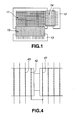
- the present invention relates to an image display apparatus, more particularly to an image display apparatus in which it is required to individually transmit a signal to a portion corresponding to a plurality of image pixels or a plurality of lines, such as a liquid crystal display, a plasma display and the like.
- the transmitting parts in which a plurality of signal lines are brought into a single element, are frequently used as a transmitting section for the above signals, as shown in Fig.1 .
- the image display apparatus is provided with an image display section 11 having a display panel such as a liquid crystal and the like, a vertical drive signal generating section 12 for generating a vertical drive image signal, a horizontal drive signal generating section 13 for generating a horizontal drive image signal, a vertical drive signal transmitting section 14 for transmitting the vertical drive image signal generated by the vertical drive signal generating section 12 to the image display section 11, and a horizontal drive signal transmitting section 15 for transmitting the horizontal drive image signal generated by the horizontal drive signal generating section 13 to the image display section 11.
- a vertical drive signal generating section 12 for generating a vertical drive image signal
- a horizontal drive signal generating section 13 for generating a horizontal drive image signal
- a vertical drive signal transmitting section 14 for transmitting the vertical drive image signal generated by the vertical drive signal generating section 12 to the image display section 11
- a horizontal drive signal transmitting section 15 for transmitting the horizontal drive image signal generated by the horizontal drive signal generating section 13 to the image display section 11.
- Each of the signal transmitting sections 14, 15 is provided with transmitting parts, for example, such as a flexible printed circuit board and the like, in which a plurality of transmitting lines for transmitting the drive signals to the respective pixels or lines of the image display section 11 are bundled parallel to each other at regular intervals.
- the pitch interval between the transmitting lines in the signal transmitting sections 14, 15 is required to be made narrow, and the number of the transmitting lines is also required to be increased.
- the signal transmitting sections 14, 15 are constituted by one printed circuit board, it is necessary to improve an accuracy of the pitch interval in order to cope with the increase of the number of the transmitting lines and the decrease of the pitch interval.
- the improvement of the accuracy of the pitch interval may result in the probability of deterioration of the production yield of the transmitting parts used for the signal transmitting sections 14, 15.
- the costs of the transmitting parts are made expensive, as a result.
- the signal transmitting sections 14, 15 are divided into a plurality of transmitting blocks 14A, 14B, 15A, 15B and 15C, respectively, as shown in Fig.2 .
- Embodiments of the present invention can provide an image display apparatus which resolves the above mentioned problem and improves the image quality.
- JP-A-04 176183 which is considered to represent the closest prior art, discloses an image display apparatus according to the precharacterizing portion of claim 1.
- an image display apparatus as defined in claim 1.
- the signal transmitting section transmits in parallel the signals for each pixel or line that is independent in the image display section.
- the capacitances between the respective transmitting lines uniform and also possible to display the image with high quality without the vertical or horizontal noise on the image.
- the signal transmitting section is divided into a plurality of transmitting blocks, it is possible to produce for each transmitting block to thereby improve the production yield.
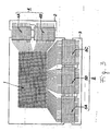
- Fig.3 is a view showing a configuration of an image display apparatus according to the present invention.
- the image display device shown in Fig.3 is provided with: an image display section 1 having a display panel, such as a liquid crystal and the like; a signal transmitting section 4 for transmitting a vertical drive image signal generated by a vertical drive signal generator 2 to the image display portion 1; and a signal transmitting section 5 for transmitting a horizontal drive image signal generated by a horizontal drive signal generator 3 to the image display section 1.
- Each of the signal transmitting sections 4, 5 is composed of transmitting parts, for example, such as a flexible printed circuit board and the like, in which a plurality of transmitting lines of transmitting the drive signals to respective pixels or lines in the image display section 1 are bundled parallel to each other at regular intervals.
- Each of the signal transmitting parts 4, 5 is divided into a plurality of transmitting blocks.
- a transmitting line on one of the transmitting blocks and a dummy transmitting line disposed in the other transmitting blocks are electrically connected to each other outside of the signal transmitting sections 4, 5.
- the transmitting line on one of the transmitting blocks and the dummy transmitting line disposed on the other transmitting blocks are electrically connected to each other on a printed board of the vertical drive signal generator 2.
- the transmitting line on one of the transmitting blocks and the dummy transmitting line disposed on the other transmitting blocks are electrically connected to each other on a printed board of the vertical drive signal generator 3.
- each of the signal transmitting sections 4, 5 a plurality of signal lines are brought into a single element for each plurality of transmitting blocks 4A, 4B, 5A, 5B and 5C.
- a transmitting line, servicing as a dummy between the transmitting lines which are located at the different transmitting blocks and adjacent to each other, is disposed in any one of the transmitting blocks including the adjacent transmitting lines.
- a transmitting line nearest to the dummy transmitting line in the other transmitting blocks of the transmitting blocks including the adjacent transmitting lines is electrically connected to the dummy transmitting line outside of the transmitting section.
- a transmitting line 41 and a transmitting line 43 are adjacent to each other in the image display apparatus 1.
- the transmitting block including the transmitting line 41 and the transmitting block including the transmitting line 43 are different from each other.
- the transmitting line 42 is the dummy transmitting line that is not used in the image display section 1, and is electrically connected to the transmitting line 41 outside of the signal transmitting section 4. Then, a distance between the dummy transmitting line 42 disposed on the signal transmitting section 4 and the normal transmitting line 43 is made equal to an interval between the transmitting lines in the respective transmitting blocks in which the transmitting line 41 and the transmitting line 43 are placed.
- the capacitance generated between the transmitting line 41 and the transmitting line 43 is equal to that generated between the transmitting lines of the respective transmitting blocks.
- the capacitances between the respective transmitting lines of the signal transmitting sections 4, 5 in which a plurality of transmitting lines are brought into the single element for each plurality of transmitting blocks can be made uniform. Therefore, it is possible to display the image with the high quality without the vertical or horizontal noise on the image. Moreover, since the signal transmitting sections 4, 5 are divided into a plurality of transmitting blocks, it is possible to produce for each transmitting block to thereby improve the production yield.
Landscapes
- Physics & Mathematics (AREA)
- Chemical & Material Sciences (AREA)
- Crystallography & Structural Chemistry (AREA)
- Engineering & Computer Science (AREA)
- Nonlinear Science (AREA)
- General Physics & Mathematics (AREA)
- Theoretical Computer Science (AREA)
- Mathematical Physics (AREA)
- Computer Hardware Design (AREA)
- Optics & Photonics (AREA)
- Devices For Indicating Variable Information By Combining Individual Elements (AREA)
- Control Of Indicators Other Than Cathode Ray Tubes (AREA)
- Liquid Crystal (AREA)
- Liquid Crystal Display Device Control (AREA)
Claims (4)
- Bildanzeigevorrichtung, mit:einem Bildanzeigeabschnitt (1), auf den ein unabhängiges Signal für jedes Pixel oder jede Zeile anwendbar ist;einem Vertikalansteuerungssignal-Erzeugungsabschnitt (2) zum Erzeugen eines Vertikalansteuerungsbildsignals;einem Horizontalansteuerungssignal-Erzeugungsabschnitt (3) zum Erzeugen eines Horizontalansteuerungsbildsignals;einem Vertikalansteuerungssignal-Übertragungsabschnitt (4) zum Übertragen des Bildsignals, das durch den Vertikalansteuerungssignal-Erzeugungsabschnitt (2) erzeugt wird, zu dem Bildanzeigeabschnitt (1); undeinem Horizontalansteuerungssignal-Übertragungsabschnitt (5) zum Übertragen des Bildsignals, das durch den Horizontalansteuerungssignal-Erzeugungsabschnitt (3) erzeugt wird, zu dem Bildanzeigeabschnitt (1);wobei eine Dummy-Übertragungsleitung (42) auf mindestens entweder dem Horizontalansteuerungssignal-Übertragungsabschnitt (5) oder dem Vertikalansteuerungssignal-Übertragungsabschnitt (4) angeordnet ist, und
wobei jeder der Signal-Übertragungsabschnitte (4, 5) die Ansteuerungssignale für jedes unabhängige Pixel oder jede unabhängige Zeile in dem Bildanzeigeabschnitt (1) parallel überträgt; und
jeder der Signal-Übertragungsabschnitte (4, 5) aus Übertragungsteilen, bei denen eine Mehrzahl von Übertragungsleitungen zum parallelen Übertragen der Ansteuerungssignale für jedes unabhängige Pixel oder jede unabhängige Zeile in dem Bildanzeigeabschnitt (1) in regelmäßigen Intervallen miteinander gebündelt sind, besteht,
wobei die Mehrzahl von Übertragungsleitungen in jedem der Signal-Übertragungsabschnitte (4, 5), die in den regelmäßigen Intervallen parallel zueinander angeordnet sind, in eine Mehrzahl von Übertragungsblöcken (4A, 4B, 5A, 5B, 5C) geteilt sind,
wobei die Dummy-Übertragungsleitung (42) in mindestens einem der Übertragungsblöcke (4A, 4B, 5A, 5B, 5C) zwischen benachbarten Übertragungsleitungen (41, 43), die sich in unterschiedlichen Übertragungsblöcken befinden, angeordnet ist, wobei die Bildanzeigevorrichtung dadurch gekennzeichnet ist, dass eine Übertragungsleitung (41) am nähesten zu der Dummy-Übertragungsleitung (42), jedoch in einem anderen Übertragungsblock, mit der Dummy-Übertragungsleitung (42) außerhalb des Signal-Übertragungsabschnitts (4, 5) elektrisch verbunden ist. - Bildanzeigevorrichtung nach Anspruch 1, bei der der Bildanzeigeabschnitt (1) aus einem Anzeigefeld, wie einer Flüssigkristallanzeige, einer Plasmaanzeige oder dergleichen, besteht.
- Bildanzeigevorrichtung nach Anspruch 1 oder 2, bei der der Übertragungsteil bei jedem der Signal-Übertragungsabschnitte (4, 5) durch eine flexible gedruckte Schaltungsplatte oder dergleichen gebildet ist.
- Bildanzeigevorrichtung nach einem der vorhergehenden Ansprüche, bei der die Dummy-Übertragungsleitung (42) eine zusätzliche Leitung ist, die zum Übertragen von Bildsignalen zwischen dem Vertikal- (2) oder Horizontal- (3) Ansteuerungssignal-Erzeugungsabschnitt und dem Bildanzeigeabschnitt (1) nicht erforderlich ist, jedoch durch den Vertikal- oder Horizontalansteuerungssignal-Erzeugungsabschnitt angesteuert wird.
Applications Claiming Priority (2)
| Application Number | Priority Date | Filing Date | Title |
|---|---|---|---|
| JP101450/96 | 1996-04-23 | ||
| JP10145096A JP3648838B2 (ja) | 1996-04-23 | 1996-04-23 | 映像表示装置 |
Publications (2)
| Publication Number | Publication Date |
|---|---|
| EP0803858A1 EP0803858A1 (de) | 1997-10-29 |
| EP0803858B1 true EP0803858B1 (de) | 2008-05-21 |
Family
ID=14301037
Family Applications (1)
| Application Number | Title | Priority Date | Filing Date |
|---|---|---|---|
| EP97302738A Expired - Lifetime EP0803858B1 (de) | 1996-04-23 | 1997-04-22 | Anzeigegerät und Zusammenbau seiner Treiberschaltung |
Country Status (5)
| Country | Link |
|---|---|
| US (1) | US5959620A (de) |
| EP (1) | EP0803858B1 (de) |
| JP (1) | JP3648838B2 (de) |
| KR (1) | KR100461746B1 (de) |
| DE (1) | DE69738703D1 (de) |
Families Citing this family (4)
| Publication number | Priority date | Publication date | Assignee | Title |
|---|---|---|---|---|
| KR100528351B1 (ko) * | 2002-12-03 | 2005-11-15 | 학교법인 한양학원 | 액정표시장치의 구동방법 및 패널구조 |
| JP2006267796A (ja) * | 2005-03-25 | 2006-10-05 | Seiko Epson Corp | 電気光学装置及び電子機器 |
| KR100708676B1 (ko) * | 2005-04-04 | 2007-04-17 | 삼성에스디아이 주식회사 | 플라즈마 디스플레이 장치 |
| JP4957190B2 (ja) * | 2006-02-21 | 2012-06-20 | セイコーエプソン株式会社 | 電気光学装置及び電子機器 |
Family Cites Families (10)
| Publication number | Priority date | Publication date | Assignee | Title |
|---|---|---|---|---|
| JP2650949B2 (ja) * | 1988-03-14 | 1997-09-10 | 株式会社日立製作所 | 液晶表示装置 |
| JPH0419617A (ja) * | 1990-05-14 | 1992-01-23 | Seiko Instr Inc | Lcdモジュールの実装構造 |
| JP3013433B2 (ja) * | 1990-11-08 | 2000-02-28 | セイコーエプソン株式会社 | 配線接続構造および電気光学装置 |
| JP2560915B2 (ja) * | 1990-11-28 | 1996-12-04 | 三菱電機株式会社 | 液晶表示パネル駆動回路 |
| JP3128826B2 (ja) * | 1990-12-25 | 2001-01-29 | 松下電器産業株式会社 | 画像表示装置 |
| KR960014823B1 (ko) * | 1991-03-15 | 1996-10-21 | 가부시기가이샤 히다찌세이사구쇼 | 액정표시장치 |
| JPH0613724A (ja) * | 1992-06-25 | 1994-01-21 | Seiko Epson Corp | 電子装置の配線構造及びそれを用いた液晶表示装置及び電子印字装置及びプラズマ表示装置及びel表示装置 |
| US5736972A (en) * | 1994-07-15 | 1998-04-07 | Sanyo Electric Co., Ltd. | Liquid crystal display apparatus capable of displaying a complete picture in response to an insufficient video signal |
| JPH0854856A (ja) * | 1994-08-10 | 1996-02-27 | Toshiba Corp | ディスプレイ装置 |
| US6169530B1 (en) * | 1995-04-20 | 2001-01-02 | Canon Kabushiki Kaisha | Display apparatus and assembly of its driving circuit |
-
1996
- 1996-04-23 JP JP10145096A patent/JP3648838B2/ja not_active Expired - Fee Related
-
1997
- 1997-04-15 US US08/839,574 patent/US5959620A/en not_active Expired - Lifetime
- 1997-04-15 KR KR1019970013715A patent/KR100461746B1/ko not_active Expired - Fee Related
- 1997-04-22 EP EP97302738A patent/EP0803858B1/de not_active Expired - Lifetime
- 1997-04-22 DE DE69738703T patent/DE69738703D1/de not_active Expired - Lifetime
Also Published As
| Publication number | Publication date |
|---|---|
| EP0803858A1 (de) | 1997-10-29 |
| US5959620A (en) | 1999-09-28 |
| JP3648838B2 (ja) | 2005-05-18 |
| KR970071440A (ko) | 1997-11-07 |
| JPH09288454A (ja) | 1997-11-04 |
| DE69738703D1 (de) | 2008-07-03 |
| KR100461746B1 (ko) | 2005-04-06 |
Similar Documents
| Publication | Publication Date | Title |
|---|---|---|
| KR100323913B1 (ko) | 반도체장치 | |
| KR100381862B1 (ko) | 액정 표시 장치 | |
| EP0397965A2 (de) | Anzeigevorrichtung | |
| EP1995718A3 (de) | Flüssigkristallanzeige und Steuerverfahren dafür | |
| US4816819A (en) | Display panel | |
| CN108267904B (zh) | 显示面板 | |
| US6937258B2 (en) | Flat panel display device | |
| EP0803858B1 (de) | Anzeigegerät und Zusammenbau seiner Treiberschaltung | |
| KR102477744B1 (ko) | 표시패널 및 표시장치 | |
| CN108267878B (zh) | 液晶显示装置 | |
| KR20150022182A (ko) | 표시 장치 | |
| KR100660446B1 (ko) | 디스플레이 드라이버를 위한 버스 배열 | |
| KR100350650B1 (ko) | 액정 표시 장치 | |
| CN112992101B (zh) | 显示系统、传输设备和中继设备 | |
| US20030169246A1 (en) | Display device and circuit board therefor including interconnection for signal transmission | |
| US6303875B1 (en) | IC packages replaceable by IC packages having a smaller pin count and circuit device using the same | |
| US20020075209A1 (en) | Image display apparatus | |
| JP2776051B2 (ja) | 半導体装置 | |
| KR20180052467A (ko) | 표시패널 및 표시장치 | |
| KR19980060012A (ko) | 액정 표시 장치 | |
| US12272285B1 (en) | Display panel, control method of display panel and display device | |
| US11615725B2 (en) | Display panel | |
| KR101032436B1 (ko) | 평판표시장치의 테이프 캐리어 패키지 및 이를 이용한 데이터 전송방법 | |
| JPH07147659A (ja) | 液晶パネル駆動回路 | |
| EP0501462A3 (de) | Anzeigegerät |
Legal Events
| Date | Code | Title | Description |
|---|---|---|---|
| PUAI | Public reference made under article 153(3) epc to a published international application that has entered the european phase |
Free format text: ORIGINAL CODE: 0009012 |
|
| AK | Designated contracting states |
Kind code of ref document: A1 Designated state(s): DE FR GB |
|
| 17P | Request for examination filed |
Effective date: 19980326 |
|
| 17Q | First examination report despatched |
Effective date: 20070612 |
|
| GRAP | Despatch of communication of intention to grant a patent |
Free format text: ORIGINAL CODE: EPIDOSNIGR1 |
|
| GRAS | Grant fee paid |
Free format text: ORIGINAL CODE: EPIDOSNIGR3 |
|
| GRAA | (expected) grant |
Free format text: ORIGINAL CODE: 0009210 |
|
| AK | Designated contracting states |
Kind code of ref document: B1 Designated state(s): DE FR GB |
|
| REG | Reference to a national code |
Ref country code: GB Ref legal event code: FG4D |
|
| REF | Corresponds to: |
Ref document number: 69738703 Country of ref document: DE Date of ref document: 20080703 Kind code of ref document: P |
|
| PLBE | No opposition filed within time limit |
Free format text: ORIGINAL CODE: 0009261 |
|
| STAA | Information on the status of an ep patent application or granted ep patent |
Free format text: STATUS: NO OPPOSITION FILED WITHIN TIME LIMIT |
|
| 26N | No opposition filed |
Effective date: 20090224 |
|
| REG | Reference to a national code |
Ref country code: GB Ref legal event code: 746 Effective date: 20120702 |
|
| REG | Reference to a national code |
Ref country code: DE Ref legal event code: R084 Ref document number: 69738703 Country of ref document: DE Effective date: 20120614 |
|
| PGFP | Annual fee paid to national office [announced via postgrant information from national office to epo] |
Ref country code: GB Payment date: 20140422 Year of fee payment: 18 |
|
| PGFP | Annual fee paid to national office [announced via postgrant information from national office to epo] |
Ref country code: FR Payment date: 20140422 Year of fee payment: 18 Ref country code: DE Payment date: 20140418 Year of fee payment: 18 |
|
| REG | Reference to a national code |
Ref country code: DE Ref legal event code: R119 Ref document number: 69738703 Country of ref document: DE |
|
| GBPC | Gb: european patent ceased through non-payment of renewal fee |
Effective date: 20150422 |
|
| PG25 | Lapsed in a contracting state [announced via postgrant information from national office to epo] |
Ref country code: DE Free format text: LAPSE BECAUSE OF NON-PAYMENT OF DUE FEES Effective date: 20151103 Ref country code: GB Free format text: LAPSE BECAUSE OF NON-PAYMENT OF DUE FEES Effective date: 20150422 |
|
| REG | Reference to a national code |
Ref country code: FR Ref legal event code: ST Effective date: 20151231 |
|
| PG25 | Lapsed in a contracting state [announced via postgrant information from national office to epo] |
Ref country code: FR Free format text: LAPSE BECAUSE OF NON-PAYMENT OF DUE FEES Effective date: 20150430 |