EP0803800B1 - Sortier- und Mischprozessor und Sortier- und Mischprozessanlage - Google Patents
Sortier- und Mischprozessor und Sortier- und Mischprozessanlage Download PDFInfo
- Publication number
- EP0803800B1 EP0803800B1 EP97106541A EP97106541A EP0803800B1 EP 0803800 B1 EP0803800 B1 EP 0803800B1 EP 97106541 A EP97106541 A EP 97106541A EP 97106541 A EP97106541 A EP 97106541A EP 0803800 B1 EP0803800 B1 EP 0803800B1
- Authority
- EP
- European Patent Office
- Prior art keywords
- data
- sort
- key
- key value
- comparison
- Prior art date
- Legal status (The legal status is an assumption and is not a legal conclusion. Google has not performed a legal analysis and makes no representation as to the accuracy of the status listed.)
- Expired - Lifetime
Links
Images




Classifications
-
- G—PHYSICS
- G06—COMPUTING OR CALCULATING; COUNTING
- G06F—ELECTRIC DIGITAL DATA PROCESSING
- G06F7/00—Methods or arrangements for processing data by operating upon the order or content of the data handled
- G06F7/22—Arrangements for sorting or merging computer data on continuous record carriers, e.g. tape, drum, disc
- G06F7/32—Merging, i.e. combining data contained in ordered sequence on at least two record carriers to produce a single carrier or set of carriers having all the original data in the ordered sequence merging methods in general
-
- G—PHYSICS
- G06—COMPUTING OR CALCULATING; COUNTING
- G06F—ELECTRIC DIGITAL DATA PROCESSING
- G06F7/00—Methods or arrangements for processing data by operating upon the order or content of the data handled
- G06F7/22—Arrangements for sorting or merging computer data on continuous record carriers, e.g. tape, drum, disc
- G06F7/36—Combined merging and sorting
Definitions
- This invention relates to a sort processor and a sort processing device for rearranging a large quantity of data, i.e. sort processing in a data base processing and a business data processing.
- a sort processor and a sort processing device are differentiated.
- a sort processor is defined as a processor for partly performing a sort processing
- a sort processing device is defined as a device for performing a complete sort processing using multiple sort processors connected in series.
- FIG. 6 shows a construction of a computer system equipped with a conventional sort processing device, which is disclosed in "Information Processing", Vol. 33, No. 12, 1992, p.p. 1416 - 1423.
- the computer system comprises a sort processing device 1, a system bus 2 of a host computer, a main storage device 3 of the host computer, a CPU 4 of the host computer, a disk drive 5 for storing a data in the host computer, and a host computer 6.
- FIG. 6 An operation of the conventional sort processing device is explained by referring to FIG. 6. Firstly, the outline of the operation is explained.
- the CPU 4 in the host computer continuously takes out data from the disk drive 5, where the object data are stored, and then continuously transmits the taken out data to the sort processing device 1 via the system bus 2.
- the main storage device 3 of the host computer 6 is used as an input-output buffer area as needed.
- the sort processing device 1 performs a sort processing when the data is inputted, and returns the result to the host computer 6 via the system bus 2.
- the host computer 6 stores the returned result data in the disk drive 5 in the same manner as that of data inputting.
- the data input to the sort processing device 1 and the output of the result data from the sort processing device 1 are performed in parallel.
- the sort processing device 1 is continuously inputted with a sequence of data transmitted by the host computer 6, rearranges the inputted data in an assigned order, and returns the result to the host computer 6. This operation is explained using FIG. 5 disclosed in the above-mentioned "Information Processing".
- FIG. 7 shows the construction of the sort processing device 1 of FIG. 6, and the sort processing device 1 is constructed by serially connecting sort processors 11, 12, 13 and 14. The respective processors 11-14 are connected to the data storage devices 15, 16, 17 and 18.
- a host computer interface 21 is used for exchanging data and instructions with the host computer 6, and a controller 19 is used for controlling the entire sort processing device 1.
- the sort processors 11-14 are called from the top a sort processor in a first stage, a sort processor in a second stage, and a sort processor in a third stage, respectively.
- a sort processor in an "i" stage has a storage capacity corresponding to a 2 i-1 data share.
- the sort processor 11 of the first stage takes out the inputted data for every two data, rearranges the data in an assigned order, and transmits the rearranged data to the sort processor of the next stage.
- the sorted data for every two data are inputted to the next stage in the order of (8,2), (3,1), (7, 5), (6,4), ... .
- the sort processor 11 of the first stage the order "1,3" of the inputted data is rearranged, and the sorted paired data in the order of (3,1) is outputted.
- the sorted combination of data like this is thereafter called as a data string or a string.
- the sort processor 12 of the second stage is inputted with these sorted data strings, takes these data strings for every pair, merges this pair of the strings, and transmits the data sorted for every four data to the next sort processor 13.
- the resulting strings become (8, 3, 2, 1), (7, 6, 5,4), ... .
- the inputted data strings (8, 2) and (3, 1) are merged to output the data string (8, 3, 2, 1).
- the sort processor 13 of the third stage is inputted with those data strings sorted for every four data, takes the strings for every pair, and transmits the data string sorted for every eight data to the sort processor 14 of the next stage.
- the result of the sort is (8, 7, 6, 5, 4, 3, 2, 1), ... .
- the sort processor 14 and succeeding sort processors perform the similar processing.
- sort processors of the respective stages it is possible for the sort processors of the respective stages to start sorting process before the sort processor of the preceding stage completes its sorting process. Therefore, when data is continuously inputed to the sort processor of the respective stages, the sort result is outputted in parallel with the data input after some delay.
- the "n" sort processors carry out the rearrangement, that is, the sorting process of the 2 n data.
- the respective sort processors utilize the connected respective data storage devices 15, 16, 17 and 18 as a storage areas in their comparison and merge processes.
- FIG. 9 shows the construction of the conventional sort processor disclosed in "Information Process” Vol. 31, No. 4, 1990, p.p. 457-465.
- FIG. 9 shows only the inside of the sort processor 12 for the simplicity of the explanation, however, the inside of the other sort processors are the same as that of the sort processor 12.
- the sort processor of FIG. 9 comprises a comparator 120 for comparing data strings, respective latch registers 121 and 122 for temporarily storing a part of a compared data, data input ports 123 and 124 for inputting the data to the comparator 120, and a controller 125 for controlling operations of the sort processors.
- the latch registers 121 and 122 have a data size equal to the comparison data size of the comparator 120 and the data width equal to that of the input ports 123 and 124. In the following explanation, this data is assumed to be 4 bytes.
- An input bus 127 inputs the data from the preceding sort processor 11, and a data and address bus 128 exchanges data with the data storage device 16 connected to the sort processor 12.
- the sort processing by the sort processor 12 is explained in detail below. The explanation is done using an example of a case when the sort processor 12 is inputted with data strings (8, 2), (3, 1), .... in sequence from the sort processor 11 of the preceding stage, the sort processor 12 merges the data strings to a data string (8, 3, 2, 1), .... and outputs the merged data string to the sort processor 13 of the next stage.
- the data string (8, 2) which is firstly inputted is stored as it is in the data storage device 16 connected to the sort processor 12.
- the data "3" of the data string (3,1) is inputted into the sort processor 12, and stored in the data storage device 16 in the same manner.
- the top data "8" in the first data string (8, 2) and the top data "3" of the data string (3, 1) are loaded from the data storage device 16 to the latch registers 121 and 122 for every 4 bytes, and comparison takes place in the comparator 120. These data are compared for every 4 bytes in sequence in this comparison.
- the sort processing if the ascending order is given as an order assignment for the sort key, the smaller comparison result is outputted first. If the descending order is given as an order assignment, the larger comparison result is outputted first.
- the controller 125 controls the ascending/ descending order for the sort key which begins from a top byte of a data. When the comparison result is determined, the data is outputted to the next sort processor 13. In parallel with this comparison process, the top data "1" of the second data string (1, 3) is stored in the data storage device 16.
- the data "8" is outputted to the sort processor 13 of the next stage. Therefore, in the following comparison, the data "3" and the data "2", which follows the "8" of the data string (8, 2), are compared. The comparison is carried out by inputting the data "3” and the data "2" to the respective latch registers 121 and 122 from the data storage device 16 for every 4 bytes, and by comparing the data for every 4 bytes.
- K is more than 2 data or data strings simultaneously without increasing the access demand to the data storage device.
- a sort processor for rearranging data strings to an assigned order is as in claim 1.
- Other aspects of the invention are as in the dependent claims.
- FIG. 1 shows a relationship of the connection between sort processors according to the present invention.
- the construction of FIG. 1 comprises sort processors 11, 12 and 13, and the respective sort processors comprise data storage devices 15, 16 and 17 for storing data strings to be sort processed.
- the respective sort processors 11, 12 and 13 comprise of four key value storing areas 131 - 134 for storing sort keys (referred to as key value below), a latch register 135, a comparator 130 and a controller 125 for controlling the entire sort processor.
- the comparator 130 can be realized by multiple comparators with 2 inputs without using a special circuit construction.
- the latch register 135 may be constructed from a general register.
- an input bus 126 is inputted with data from the sort processor 11 of the preceding stage, an output bus 127 outputs data to the sort processor 13 of the succeeding stage, and an address and data bus 128 exchanges data with data storage device 16 connected to the sort processor 12.
- the comparator 130 includes input ports 136 - 140.
- the latch register 135 is a register having a bit width which the comparator 130 compares at one time.
- the key value storage device 131 - 134 are constructed by such as register files and memory elements having a capacity to store all the key value of data.
- the key value storage device 131, 132, 133 and 134 are called as a first, a second, a third and a forth key value storage device respectively for the convenience of explanation.
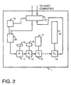
- FIG. 2 shows a sort processing device constructed with the sort processors according to the present invention.
- a sort processing device 1 comprises sort processors 11 - 14, data storage devices 15 - 18 for the respective sort processors, an interface portion 21 for exchanging data and processing demand with the host computer, a key converter 20 for converting the key value of data, and a sort processing device controller 19 for controlling the sort processing device 1 as a whole.
- the key converter 20 is constructed to connect to the sort processor 11 of the first stage.
- FIG. 2 The construction of FIG. 2 is similar to that of FIG. 7 in which the conventional example is explained. However, the capacity of the data storage devices 15, 16, 17 and 18 added to the respective sort processors, and the internal structure of the respective sort processors in FIG. 2 are different from those of the conventional art in FIG. 6.
- the sort processing device 1 is continuously inputted with a series of data transmitted from the host computer, rearranges, and returns the result to the host computer.
- the sort processor group 11, 12, 13 and 14 is linearly connected to the data storage device group 15, 16, 17 and 18 which is added to the respective sort storage group, and the key converter 20 is connected prior to the sort processor 11 in the first stage.
- the rearrangement of data is performed based on the key values of the data. For example, assuming that the format of an object data is as shown below and only the sorting process in a descending order is possible, it is explained below how data are rearranged.
- Data format key 1 + key 2 + key 3 + non-key data; Where, the key 1 and key 3 are assumed to be assigned as an ascending order, and the key 2 is assumed to be assigned as a descending order.
- the controller 19 receives the assignment of either ascending or descending orders regarding the keys 1 - 3 from the host computer. Then the controller 19 interprets the order and controls the key converter 20 to output the data to the first sort processor 11 by inverting their bits, regarding the key 1 and key 3 out of the inputted respective data. This process makes it possible to sort multiple keys having both ascending and descending orders, as shown in the example below, even if the sort processors only have the function for sorting in a descending order.
- the controller 19 sends an order to the key converter 20 to perform the bit-inversion on, in this example, the key 2.
- the sort processors are respectively defined from the top as a sort processor of a first stage (P 1 ), a sort processor of a second stage (P 2 ), a sort processor of a third stage (P 3 ) and so on.
- data are inputted to the sort processing device 1 in the order of: 8, 2, 1, 3, 5, 7, 6, 4, 9, 0, 8, 5, 1, 10, 3, 4, ....
- the sort processor 11 of the first stage from the top takes out the inputted data for every four data, and rearranges and transmits those four data to the sort processor 12 of the succeeding stage.
- the data sorted for every four data are inputted to the sort processor 12 of the succeeding stage in the order of:
- the sort processor 12 of the second stage is inputted with those data grouped by four data, takes those grouped data for every four data, transmits the data sequences sorted by every 16 to the sort processor 13 of the succeeding stage.
- the result is:
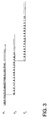
- the sort processor 13 of the third stage performs the same process. This process is shown in FIG. 3. As shown in FIG. 3, it is possible for the processors of the respective stages to start its process before the processor of the preceding stage completes its process. Therefore, when data are inputted continuously, the sort result is outputted with a little delay time in parallel to the input of the data.
- n sort processors rearranges K n data, that is, performs sorting processes on K n data.
- the sort of N data is achieved by log K N sort processors.
- twenty sort processors have been necessary.
- the respective sort processors of the present invention uses the data storage devices 15, 16, 17 and 18 which are connected to the respective sort processors as a storage region.
- sort processor 12 is inputted with the data strings (8, 3, 2, 1), (7, 6, 5, 4), (9, 8, 5, 0), (10, 4, 3, 1), conceivabl from the sort processor 11 of the preceding stage.
- the sort processor 12 then merges these data strings to form a data string (10, 9, 8, 8, 7, 6, 5, 5, 4, 4, 3, 3, 2, 1, 1, 0)...., and outputs the data string to the sort processor 13 of the succeeding stage.
- the data strings (8, 3, 2, 1), (7, 6, 5, 4), (9, 8, 5, 0) are inputted to the sort processor 12 from the input bus 126 and stored in the data storage device 16 connected to the sort processor 12, maintaining their order.
- the key values of the top data "8" of the data string (8, 3, 2, 1), the top data "7” of the data string (7, 6, 5, 4) and the top data "9” of the data string (9, 8, 5, 0) are stored in the key value storage device 131, 132 and 133, respectively.
- the fourth key value storage device 134 out of the four key storages is left empty.
- the key value of the fourth data string (10, 4, 3, 1) is stored.
- corresponding key value storage device is assigned to the key value of the respective data strings and fixed as follows.
- the controller 125 controls the comparator 130 to compare the data inputted from the first, second and third key storages 131, 132, 133 corresponding to the first K- 1 key values where key values are stored, with the data (key values) of the latch register 135.
- the fourth remaining data string (10, 4, 3, 1) is inputted in sequence to the input bus 126 from the sort processor 11 of the preceding stage.
- the sort processor 12 stores the key value of its top data "10" for every 4 bytes in the latch register 135 in sequence, and compares it with the data stored in the key value storage devices 131, 132, 133 in every 4 byes. Simultaneously, the key value portion of the inputted data is stored in the key value storage device 134 which has been left empty.
- the comparison begins in the comparator 130 simultaneously.
- the key value of the data "10” is stored in the latch register 135 for every four bytes.
- the data "10” may also be stored in the data storage device 16 in the same manner as other data strings.
- a data comprises a key portion and a non-key portion, for example, each data 8, 9, 2, 1 in a set of data (8, 9, 2, 1) indicates only the key portion.
- the key portion is succeeded with the non-key portion such as ([8, abc], [9, def], [2, abc], [1, xyz]), wherein "abc", "def”, "abc”,”xyz” indicate the non-key portions.
- the non-key portion of the data inputted from the data input bus 126 is outputted as it is to the sort processor 13 of the succeeding stage via the data output bus 127.
- the data "4" following the data "10” in the fourth data string is inputted from the input bus 126.
- This data "4" is inputted to the latch register 135 for every four bytes, in the same manner as that of the data "10”, and is compared for every four bytes with the data "8", "7” and "9” stored in the key value storage devices 131, 132 and 133.
- the key value of this data "4" is stored in the key value storage device 134 which had been left empty.
- the data "9" stored in the key value storage device 133 is outputted as a result of the comparison instead of the data inputted to the latch register 135. Therefore, in this case, the key portion of the data "9” is outputted to the sort processor 13 of the succeeding stage from the comparator 130 via the data output bus 127. If there is a non-key data portion of the data "9”, the non-key portion of the data "9” is read our from the data storage device 16 and outputted to the sort processor 13 of the succeeding stage via the data output bus 127.
- this data portion is transmitted from the sort processor 11 of the preceding stage via the data input bus 126, and is sent to the data storage device 16 and stored therein.
- the controller 125 controls the comparator 130 to compare the data from the data input ports 136, 137, 139 and 140.
- the key value of the data "8”, which follows the data "9” in the data string (9, 8, 5, 0) is read out for every four bytes and stored in the latch register 135, which is connected to the comparator 130.
- the comparator 130 compares the stored data with the data "8", "7” and "4" stored in the other key value storage devices 131, 132 and 134 for every four bytes. This comparing operation starts simultaneously when the first four bytes of the key value of the data "8" are stored to the latch register 135.
- the key value of the data "8” is stored in the latch register 135, while at the same time it is stored in the key value storage device 133.
- the data "3 " which follows the data "4" in the data string (10, 4, 3, 1) transmitted from the sort processor 11 of the preceding stage via the data input bus 126 is stored in the data storage device 16.
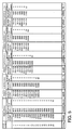
- FIG. 4 shows a data flow in the above-explained sort processing.
- the key value of the data "10” is shown as 10 K
- the first and the second four bytes of the key value of the data "10” are shown as 10 K -1 and 10 K -2.
- the key value is assumed to be 8 bytes (4 byte ⁇ 2).
- the time is assumed to go to right direction through the horizontal axis.
- the FIG. 4 also shows an operational state of the sort processor in the second stage.
- the data is inputted from the preceding stage to the input bus 126 in the order of 8, 3, 2, 1, 7, 6, 5, 4, ... .
- This input dada from the preceding stage is shown in the top line of FIG. 4.
- These data are grouped for every sorted data as shown in the following.
- top data of respective sets of data are written in the corresponding key storage devices, for example, the top data "8" of the data set (8, 3, 2, 1) is written in the key storage device 131, the top data "7” of the data set (7, 6, 5, 4) is written in the key storage device 132, the top data "9” of the data set (9, 8, 5, 0) is written in the key storage device 133, the top data "10" of the data set (10, 4, 3, 1) is written in the key storage device 134 as shown in the third line to sixth line of FIG. 4 corresponding to the time of 1, 5, 9, 13 of the horizontal axis.
- the key "10" is stored in the latch register 135 for every four bytes at the same time when the key "10" is stored into the key storage device 134.
- each top data "8", “7”,” 9" in the key storage device 131 ⁇ 133 and the data "10” in the latch register 135 are compared.
- the contents in the key storage device 131 ⁇ 133 and the content in the latch register is effective, and the content in the key storage device 135 where the last data is stored is non-effective.
- the data "10" having the maximum value is selected and outputted to the output bus 127.
- the key portion of "4" is stored in the key storage device 134 where the data "10" have been stored.
- the key "4" is stored in the latch register 135 for every four bytes at the same time when the key "4" is stored into the key storage device 134.
- each top data "8", “7”,” 9" in the key storage device 131 ⁇ 133 and the data "4" in the latch register 135 are compared at the time 14 in the horizontal axis.
- the contents in the key storage device 131 ⁇ 133 and the content in the latch register is effective, and the content in the key storage device 133 where the last data is stored is also non-effective.
- the data "9" having the maximum value between the compared data is selected and outputted to the output bus 127.
- the key portion of "8" is stored in the key storage device 133 where the data "9” have been stored.
- the key "5" is stored in the latch register 135 for every four bytes at the same time when the key "5" is stored into the key storage device 133.
- each top data "8", “7” in the key storage devices 131, 132 and the data "5" in the latch register 135 are compared at the time 15 in the horizontal axis.
- the contents in the key storage devices 131, 132, 134 and the content in the latch register 135 is effective, and the content in the key storage device 133 where the last data is stored is also non-effective.
- the data "8" having the maximum value between the compared data is selected and outputted to the output bus 127.
- the controller 125 uses the bus connected to the key value storage devices by means of time sharing.
- the data storage device 16, the key value storage device 131-134 and the latch register 135 may be connected by separate buses.
- the sort processing is completed.
- the data on the four strings disappear.
- the data strings (8, 3, 2, 1), (7, 6, 5, 4), (9, 8, 5, 0), (10, 4, 3, 1) .... are inputted, and the sort processor 12 merges these four strings to output the data string (10, 9, 8, 8, 7, 6, 5, 5, 4, 3, 3, 2, 1, 1, 0), ... .
- the data on the second data string (7, 6, 5, 4) disappears from this sort processor 12.
- the controller 125 controls the comparator 130 so that the corresponding key value storage device does not become the object of comparison for this data string.
- the constructions of the data storage devices 15 - 18 are explained below.
- the data storage devices 15 - 18 are constructed by the normal DRAM.
- FIG. 5 the relation between the data storage device and the number of DRAMs necessary is shown in case that the comparation data at a time is changed.
- the present invention is able to reduce the amount of hardware.
- the hardware scale of the sort processing device can be reduced, at the same time it is also possible to minimize the sort processing device for sorting a constant amount of data.
- the performance does not deteriorate even if the number of the access to the data storage device is increased.
- the sort processor simply performs a sort in a descending or an ascending order by inverting sign bits of any small keys in the preceding process. For example, if the key is as "00010100" in which the value "0001" of the first small key is assigned in the ascending order and the value "0100" of the second small key is assigned in the descending order, the value of the second key is inverted such as "1011" and the key including both the first small key and the second small key such as "00011010" is sent to the sort processor. In this case, the sort processor simply performs the sort in the ascending order by using the single ascending key comprised of two bites value "00011010". Therefore, the hardware of the sort processor can be simplified.
Landscapes
- Engineering & Computer Science (AREA)
- General Engineering & Computer Science (AREA)
- Theoretical Computer Science (AREA)
- Computer Hardware Design (AREA)
- Physics & Mathematics (AREA)
- General Physics & Mathematics (AREA)
- Multi Processors (AREA)
- Information Retrieval, Db Structures And Fs Structures Therefor (AREA)
- Complex Calculations (AREA)
Claims (14)
- Sortierprozessor (11) zum Sortieren von Datenketten in einer zugewiesenen Sortierfolge, welcher aufweist:dadurch gekennzeichnet, dasseine erste Datenspeichervorrichtung (16) zum Speichern von K sortierten Eingangsdatenketten, wobei K eine ganze Zahl größer als oder gleich 2 ist;einen Komparator (130),der Komparator (130) K+1 Eingangstore hat für die Eingabe von Vergleichsobjektdaten von kontinuierlichen K Sätzen der Datenketten, die angeordnet sind zum selektiven Vergleichen von Daten von K der K+1 Tore; dassder Sortierprozessor (11) weiterhin eine Steuervorrichtung (125) aufweist, die ausgebildet ist zum Auswählen der K Eingangstore, die in den Komparator (130) führen; und dassK Eingangstore der K+1 Tore des Komparators (130) ausgerüstet sind mit jeweiligen weiteren Datenspeichervorrichtungen (131 - 134), von denen jede ausgebildet ist zum Speichern mehrerer Daten, die Objekt für den Vergleich sind, das verbleibende Eingangstor ausgerüstet ist mit einem einzelnen Datenregister (135), wobei die K Daten, die verglichen werden, K-1 Daten, die von jeweiligen K-1 Eingangstoren der K Eingangstore eingegeben sind, und von dem Register eingegebene Daten sind.
- Sortierprozessor (11) nach Anspruch 1, die so ausgebildet sind, dass die Datenspeichervorrichtungen (131 - 134) nur Schlüsselwerte von verglichenen Daten speichern.
- Sortierprozessor (11) nach Anspruch 2, bei dem die K Datenreihen jeweils den K weiteren Speichervorrichtungen zum Speichern der Schlüsselwerte der Daten entsprechen.
- Sortierprozessor (11) nach Anspruch 2, der so ausgebildet ist, dass bei einer Vorverarbeitung für den Vergleichsvorgang die Steuervorrichtung (125) die Schlüsselwerte von ersten K-1 Datenreihen aus den K Datenreihen, die das Objekt des Vergleichs sind, in jeweiligen ersten K-1 Schlüsselwert-Speichervorrichtungen der K Schlüsselwert-Speichervorrichtungen speichert, und zur selben Zeit der höchste der Schlüsselwerte der K-ten Daten in dem Register (135) gespeichert wird, und der Sortierprozessor weiterhin so ausgebildet ist, dass die Steuervorrichtung (125) die Eingangstore entsprechend den ersten K-1 Schlüsselwert-Speichervorrichtungen und das mit dem Register (135) verbundene Eingangstor auswählt, um den Vergleichsvorgang zu beginnen, und die Schlüsselwerte der K-ten Datenkette in der K-ten Schlüsselwert-Speichervorrichtung speichert.
- Sortierprozessor (11) nach Anspruch 4, der so ausgebildet ist, dass am Beginn des ersten Vergleichsvorgangs die Steuervorrichtung (125) die höchsten Daten der jeweiligen Datenketten in der Datenspeichervorrichtung speichert, während sie die K-1 Datenketten aus K Datenketten, die Objekt des Vergleichs sind, in der Datenspeichervorrichtung speichert, und sie die Schlüsselwerte entsprechend den jeweiligen Daten parallel in den Schlüsselwert-Speichervorrichtungen speichert.
- Sortierprozessor (11) nach Anspruch 2, welcher so ausgebildet ist, dass in den Vergleichsvorgängen nachfolgend dem ersten Vergleichsvorgang der wiederholt von jeweiligen Sortierprozessoren (11 - 14) durchgeführten Vergleichsvorgänge der Komparator (130) aus den Ergebnissen des Vergleichs von den Schlüsseldaten von K Daten auswählt, welche Daten zu dem Sortierprozessor (11) in der nächsten Stufe auszugeben sind, und dann der Komparator (130) den Schlüsselwert der folgenden Daten in der Datenkette der ausgegebenen Daten in dem Register (135) speichert, um den nächsten Vergleichsvorgang zu beginnen, und auch diesen Schlüsselwert an der Stelle der Schlüsselwert-Speichervorrichtung speichert, an der der Schlüsselwert der ausgegebenen Daten gespeichert war.
- Sortierprozessor (11) nach Anspruch 6, bei dem der Komparator (130) so ausgebildet ist, dass er die kleinsten Daten oder die größten Daten auswählt.
- Sortierprozessor (11) nach Anspruch 6, welcher so ausgebildet ist, dass für den Fall, dass die in dem Register (135) gespeicherten Daten gemäß dem Ergebnis des Vergleichs durch den Komparator (130) ausgegeben werden, die Steuervorrichtung (125) den Schlüsselwert der Daten folgend den ausgegebenen Daten in der Datenkette, zu der die ausgegebenen Daten gehören, in dem Register (135) speichert, um den Vergleichsvorgang des Komparators (130) zu beginnen, zu derselben Zeit, zu der dieser Schlüsselwert an der Stelle der Schlüsselwert-Speichervorrichtung, an der der Schlüsselwert der ausgegebenen Daten gespeichert war, gespeichert wird.
- Sortierprozessor (11) nach Anspruch 2, welcher so ausgebildet ist, dass, wenn keine weiteren Daten in der Datenkette der ausgegebenen Daten als ein Ergebnis des Vergleichs in dem Komparator (130) vorhanden sind, die Steuervorrichtung (125) danach nicht mehr das Eingangstor des Komparators (130) entsprechend der Schlüsselwert-Speichervorrichtung, in der der Schlüsselwert der ausgegebenen Daten gespeichert war, auswählt.
- Sortierprozessor (11) nach Anspruch 1, bei dem der Wert von K definiert ist als K=2n, wobei n eine ganze Zahl größer als oder gleich 2 ist.
- Sortierprozessorvorrichtung (11), bei der mehrere Sortierprozessoren (11 - 14) entsprechend Anspruch 1 in einem Halbleiterchip integriert sind.
- Sortierprozessorvorrichtung (1), bei der mehrere Sortierprozessoren (11 - 14) nach Anspruch 1 in Reihe verbunden sind.
- Sortierprozessorvorrichtung (1) nach Anspruch 12, welche weiterhin aufweist:einen Schlüsselumwandler (20) zum Invertieren der Bits von Schlüsselwerten, die in einer Reihenfolge angeordnet sind, die entgegengesetzt zu der der Vergleichsfunktion des Komparators (130) ist, bevor der invertierte Schlüsselwert zu dem Sortierprozessor (11) einer ersten Stufe übertragen wird.
- Sortierprozessorvorrichtung (1) welche aufweist:mehrere Sortierprozessoren (11 - 14) nach einem der Ansprüche 2 - 9, die so ausgebildet sind, dass die mehreren Sortierprozessoren (11 - 14) parallel arbeiten und wiederholt Vergleichsvorgänge unter Verwendung jeweiliger Komparatoren (130) durchführen, um einen Sortiervorgang bei einer Vielzahl von Daten durchzuführen; undeinen Schlüsselumwandler (20) zum Invertieren der Bits von Schlüsselwerten, die in einer Reihenfolge angeordnet sind, die derjenigen der Vergleichsfunktion des Komparators (130) entgegengesetzt ist, bevor der invertierte Schlüsselwert zu einem Sortierprozessor (11) einer ersten Stufe übertragen wird.
Applications Claiming Priority (3)
| Application Number | Priority Date | Filing Date | Title |
|---|---|---|---|
| JP107001/96 | 1996-04-26 | ||
| JP10700196 | 1996-04-26 | ||
| JP10700196A JP3196637B2 (ja) | 1996-04-26 | 1996-04-26 | ソートプロセッサおよびソート処理装置 |
Publications (3)
| Publication Number | Publication Date |
|---|---|
| EP0803800A2 EP0803800A2 (de) | 1997-10-29 |
| EP0803800A3 EP0803800A3 (de) | 1997-12-03 |
| EP0803800B1 true EP0803800B1 (de) | 2004-07-14 |
Family
ID=14447976
Family Applications (1)
| Application Number | Title | Priority Date | Filing Date |
|---|---|---|---|
| EP97106541A Expired - Lifetime EP0803800B1 (de) | 1996-04-26 | 1997-04-21 | Sortier- und Mischprozessor und Sortier- und Mischprozessanlage |
Country Status (5)
| Country | Link |
|---|---|
| US (1) | US5903780A (de) |
| EP (1) | EP0803800B1 (de) |
| JP (1) | JP3196637B2 (de) |
| DE (1) | DE69729818T2 (de) |
| TW (1) | TW366467B (de) |
Families Citing this family (10)
| Publication number | Priority date | Publication date | Assignee | Title |
|---|---|---|---|---|
| US6370676B1 (en) * | 1999-05-27 | 2002-04-09 | International Business Machines Corporation | On-demand process sorting method and apparatus |
| CA2348239C (en) * | 2001-05-18 | 2005-04-19 | Ibm Canada Limited-Ibm Canada Limitee | Culturally correct ordering of keyed records |
| AU2003231521A1 (en) * | 2002-04-26 | 2003-11-10 | Nihon University School Juridical Person | Parallel merge/sort processing device, method, and program |
| ATE543138T1 (de) * | 2002-07-23 | 2012-02-15 | St Ericsson Sa | Verbesserte interprozessorkommunikation zwischen prozessoren |
| JP2005190047A (ja) * | 2003-12-25 | 2005-07-14 | Hitachi Ltd | データソート機能を持つストレージシステム |
| JP6380952B2 (ja) | 2014-12-12 | 2018-08-29 | インターナショナル・ビジネス・マシーンズ・コーポレーションInternational Business Machines Corporation | 多数の要素からなる配列をソートする装置、方法およびプログラム |
| US10936283B2 (en) * | 2017-11-30 | 2021-03-02 | International Business Machines Corporation | Buffer size optimization in a hierarchical structure |
| US11048475B2 (en) | 2017-11-30 | 2021-06-29 | International Business Machines Corporation | Multi-cycle key compares for keys and records of variable length |
| US11354094B2 (en) | 2017-11-30 | 2022-06-07 | International Business Machines Corporation | Hierarchical sort/merge structure using a request pipe |
| US10896022B2 (en) | 2017-11-30 | 2021-01-19 | International Business Machines Corporation | Sorting using pipelined compare units |
Family Cites Families (8)
| Publication number | Priority date | Publication date | Assignee | Title |
|---|---|---|---|---|
| US3713107A (en) * | 1972-04-03 | 1973-01-23 | Ncr | Firmware sort processor system |
| US4410960A (en) * | 1980-02-05 | 1983-10-18 | Nippon Electric Co., Ltd. | Sorting circuit for three or more inputs |
| JPS59123048A (ja) * | 1982-12-28 | 1984-07-16 | Toshiba Corp | ソ−ト処理装置 |
| US4567572A (en) * | 1983-02-22 | 1986-01-28 | The United States Of America As Represented By The Director Of The National Security Agency | Fast parallel sorting processor |
| DE3322706A1 (de) * | 1983-06-24 | 1985-01-10 | Fa. Carl Zeiss, 7920 Heidenheim | Schaltungsanordnung zur schnellen rangordnungsauswahl oder -sortierung |
| JPS6237739A (ja) * | 1985-08-12 | 1987-02-18 | Nippon Telegr & Teleph Corp <Ntt> | ソ−ト処理装置 |
| JPS63304318A (ja) * | 1987-06-04 | 1988-12-12 | Nec Corp | 多入力比較回路 |
| JP2752634B2 (ja) * | 1988-05-26 | 1998-05-18 | 優 喜連川 | ソート処理装置 |
-
1996
- 1996-04-26 JP JP10700196A patent/JP3196637B2/ja not_active Expired - Fee Related
-
1997
- 1997-03-18 TW TW086103345A patent/TW366467B/zh not_active IP Right Cessation
- 1997-04-03 US US08/834,738 patent/US5903780A/en not_active Expired - Fee Related
- 1997-04-21 DE DE69729818T patent/DE69729818T2/de not_active Expired - Fee Related
- 1997-04-21 EP EP97106541A patent/EP0803800B1/de not_active Expired - Lifetime
Also Published As
| Publication number | Publication date |
|---|---|
| DE69729818T2 (de) | 2005-07-07 |
| TW366467B (en) | 1999-08-11 |
| US5903780A (en) | 1999-05-11 |
| JP3196637B2 (ja) | 2001-08-06 |
| EP0803800A3 (de) | 1997-12-03 |
| EP0803800A2 (de) | 1997-10-29 |
| DE69729818D1 (de) | 2004-08-19 |
| JPH09292975A (ja) | 1997-11-11 |
Similar Documents
| Publication | Publication Date | Title |
|---|---|---|
| US5590353A (en) | Vector processor adopting a memory skewing scheme for preventing degradation of access performance | |
| US5410727A (en) | Input/output system for a massively parallel, single instruction, multiple data (SIMD) computer providing for the simultaneous transfer of data between a host computer input/output system and all SIMD memory devices | |
| US4751671A (en) | Size configurable data storage system | |
| EP1345125A2 (de) | DRAM-system mit Bankenkonfliktvermeidungsfähigkeit | |
| US20040172581A1 (en) | External storage device and memory access control method thereof | |
| CN100380351C (zh) | 获得数据掩码映射信息 | |
| US20030037209A1 (en) | Memory engine for the inspection and manipulation of data | |
| Wuytack et al. | Flow graph balancing for minimizing the required memory bandwidth | |
| US5903780A (en) | Data sorting device having multi-input comparator comparing data input from latch register and key value storage devices | |
| KR0174266B1 (ko) | 반도체기억장치 | |
| CN1653435B (zh) | 用于在硬件中映射数据掩码的装置、方法和系统 | |
| EP0961966B1 (de) | N-weg verarbeitung von bitketten in einer datenflussarchitektur | |
| US4796222A (en) | Memory structure for nonsequential storage of block bytes in multi-bit chips | |
| US7617383B2 (en) | Circular register arrays of a computer | |
| US5802565A (en) | Speed optimal bit ordering in a cache memory | |
| US6266796B1 (en) | Data ordering for cache data transfer | |
| US5659733A (en) | Sort processing method and apparatus for sorting data blocks using work buffer merge data records while sequentially transferring data records from work buffers | |
| US5201058A (en) | Control system for transferring vector data without waiting for transfer end of the previous vector data | |
| KR920003176B1 (ko) | 정렬처리장치의 제어데이타 생성장치 | |
| US4992979A (en) | Memory structure for nonsequential storage of block bytes in multi bit chips | |
| KR20030064391A (ko) | 대규모 병렬 프로세서 어레이를 메모리 어레이에 비트직렬 방식으로 접속하는 방법 및 장치 | |
| US7502920B2 (en) | Hierarchical storage architecture for reconfigurable logic configurations | |
| JPH0482082A (ja) | 半導体記憶装置 | |
| EP0359192B1 (de) | Vektorprozessoren und Vektorregistersteuerung | |
| EP1585024B1 (de) | Ein verbesserter on-chip Speicher zur Speicherung von variablen Datenbits |
Legal Events
| Date | Code | Title | Description |
|---|---|---|---|
| PUAI | Public reference made under article 153(3) epc to a published international application that has entered the european phase |
Free format text: ORIGINAL CODE: 0009012 |
|
| PUAL | Search report despatched |
Free format text: ORIGINAL CODE: 0009013 |
|
| AK | Designated contracting states |
Kind code of ref document: A2 Designated state(s): DE FR GB |
|
| AK | Designated contracting states |
Kind code of ref document: A3 Designated state(s): DE FR GB |
|
| 17P | Request for examination filed |
Effective date: 19980514 |
|
| 17Q | First examination report despatched |
Effective date: 20020517 |
|
| GRAP | Despatch of communication of intention to grant a patent |
Free format text: ORIGINAL CODE: EPIDOSNIGR1 |
|
| GRAS | Grant fee paid |
Free format text: ORIGINAL CODE: EPIDOSNIGR3 |
|
| GRAA | (expected) grant |
Free format text: ORIGINAL CODE: 0009210 |
|
| AK | Designated contracting states |
Kind code of ref document: B1 Designated state(s): DE FR GB |
|
| REG | Reference to a national code |
Ref country code: GB Ref legal event code: FG4D |
|
| REF | Corresponds to: |
Ref document number: 69729818 Country of ref document: DE Date of ref document: 20040819 Kind code of ref document: P |
|
| ET | Fr: translation filed | ||
| PLBE | No opposition filed within time limit |
Free format text: ORIGINAL CODE: 0009261 |
|
| STAA | Information on the status of an ep patent application or granted ep patent |
Free format text: STATUS: NO OPPOSITION FILED WITHIN TIME LIMIT |
|
| 26N | No opposition filed |
Effective date: 20050415 |
|
| PGFP | Annual fee paid to national office [announced via postgrant information from national office to epo] |
Ref country code: DE Payment date: 20070419 Year of fee payment: 11 |
|
| REG | Reference to a national code |
Ref country code: GB Ref legal event code: 746 Effective date: 20070416 |
|
| PGFP | Annual fee paid to national office [announced via postgrant information from national office to epo] |
Ref country code: GB Payment date: 20070418 Year of fee payment: 11 |
|
| PGFP | Annual fee paid to national office [announced via postgrant information from national office to epo] |
Ref country code: FR Payment date: 20070411 Year of fee payment: 11 |
|
| GBPC | Gb: european patent ceased through non-payment of renewal fee |
Effective date: 20080421 |
|
| PG25 | Lapsed in a contracting state [announced via postgrant information from national office to epo] |
Ref country code: DE Free format text: LAPSE BECAUSE OF NON-PAYMENT OF DUE FEES Effective date: 20081101 |
|
| REG | Reference to a national code |
Ref country code: FR Ref legal event code: ST Effective date: 20081231 |
|
| PG25 | Lapsed in a contracting state [announced via postgrant information from national office to epo] |
Ref country code: FR Free format text: LAPSE BECAUSE OF NON-PAYMENT OF DUE FEES Effective date: 20080430 |
|
| PG25 | Lapsed in a contracting state [announced via postgrant information from national office to epo] |
Ref country code: GB Free format text: LAPSE BECAUSE OF NON-PAYMENT OF DUE FEES Effective date: 20080421 |