EP0802541A1 - Verfahren, um redundante fehlerhafte Adressen in einer Speicheranordnung mit Redundanz zu erkennen - Google Patents
Verfahren, um redundante fehlerhafte Adressen in einer Speicheranordnung mit Redundanz zu erkennen Download PDFInfo
- Publication number
- EP0802541A1 EP0802541A1 EP96830216A EP96830216A EP0802541A1 EP 0802541 A1 EP0802541 A1 EP 0802541A1 EP 96830216 A EP96830216 A EP 96830216A EP 96830216 A EP96830216 A EP 96830216A EP 0802541 A1 EP0802541 A1 EP 0802541A1
- Authority
- EP
- European Patent Office
- Prior art keywords
- group
- memory
- defective
- redundancy
- current address
- Prior art date
- Legal status (The legal status is an assumption and is not a legal conclusion. Google has not performed a legal analysis and makes no representation as to the accuracy of the status listed.)
- Granted
Links
- 230000002950 deficient Effects 0.000 title claims abstract description 89
- 238000000034 method Methods 0.000 title claims abstract description 24
- 230000015654 memory Effects 0.000 claims abstract description 124
- 230000003213 activating effect Effects 0.000 claims abstract description 18
- 230000004913 activation Effects 0.000 claims abstract description 8
- 238000012360 testing method Methods 0.000 claims description 15
- 238000001514 detection method Methods 0.000 claims 1
- 239000011159 matrix material Substances 0.000 description 8
- 230000007704 transition Effects 0.000 description 8
- 230000009977 dual effect Effects 0.000 description 5
- 238000007796 conventional method Methods 0.000 description 3
- 230000000295 complement effect Effects 0.000 description 1
- 239000004065 semiconductor Substances 0.000 description 1
- 238000006467 substitution reaction Methods 0.000 description 1
Images


Classifications
-
- G—PHYSICS
- G11—INFORMATION STORAGE
- G11C—STATIC STORES
- G11C29/00—Checking stores for correct operation ; Subsequent repair; Testing stores during standby or offline operation
- G11C29/70—Masking faults in memories by using spares or by reconfiguring
- G11C29/78—Masking faults in memories by using spares or by reconfiguring using programmable devices
- G11C29/835—Masking faults in memories by using spares or by reconfiguring using programmable devices with roll call arrangements for redundant substitutions
-
- G—PHYSICS
- G11—INFORMATION STORAGE
- G11C—STATIC STORES
- G11C29/00—Checking stores for correct operation ; Subsequent repair; Testing stores during standby or offline operation
- G11C29/04—Detection or location of defective memory elements, e.g. cell constructio details, timing of test signals
- G11C29/08—Functional testing, e.g. testing during refresh, power-on self testing [POST] or distributed testing
- G11C29/12—Built-in arrangements for testing, e.g. built-in self testing [BIST] or interconnection details
- G11C29/44—Indication or identification of errors, e.g. for repair
Definitions
- redundancy memory elements such as redundancy word lines and/or bit lines, useful for functionally replacing defective word lines or bit lines.
- non-volatile memory registers redundancy registers
- redundancy registers must be provided in the memory device for storing the addresses of the defective memory elements (defective addresses), and for comparing a current address supplied to the memory device with the defective addresses stored therein: when the current address coincides with a defective address, the defective memory element is not selected, and a redundancy memory element is instead selected; if this occurs, it is said that the defective memory element has been redunded.
- redundancy memory element for a defective memory element is completely transparent to the end user, but the memory device manufacturer could be interested in knowing which of the memory elements are defective, i.e. which are the defective addresses.
- output signals of the redundancy registers i.e. the signals representative of the condition of coincidence between the current address supplied to the memory device and one of the defective addresses stored therein
- the redundancy registers are logically OR-ed together and the resulting signal is directly supplied to an output terminal of the memory device; the memory device is sequentially supplied with all the possible address configurations: when the current address configuration coincides with a defective address, a transition is detected at the output terminal, indicating that the current address is a defective address.
- a method for detecting redunded defective addresses in a memory device with redundancy comprising at least one memory register for storing at least one defective address, said memory register comprising a plurality of memory units each one storing a defective address bit and comparing said defective address bit with a respective current address bit of a current address supplied to the memory device, the memory register activating a respective redundancy selection signal when the current address coincides with the at least one defective address stored therein, characterized by providing for:
- the present invention provides a faster method to detect redunded defective addresses, because instead of scanning all the possible address configurations it provides for scanning a first subset of address bits, detecting which configurations of ths subset of address bits are defective and, only for those configurations, scanning the remaining subset of address bits.
- the number of configurations to be scanned is thus substantially smaller than the overall number of address configurations of the memory device, thus allowing a significant time saving.
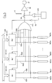
- Fig. 1 schematically shows a programmable memory register (redundancy register) provided in a memory device to implement redundancy.
- the redundancy register RR comprises a plurality of programmable memory units MU0-MU10, each one capable of storing a binary information unit.
- Each one of the memory units MU0-MU10 is supplied by a respective address signal A0-A10 taken from an address signal bus ADD of the memory device.
- memory devices comprise a matrix of memory cells arranged in row (word lines) and columns (bit lines); A0-A10 can be for example the row address signals which are decoded for selecting one of the word lines of the memory matrix; in alternative, A0-A10 can be the column address signals which are decoded for selecting one of the bit lines of the memory matrix. As shown schematically in Fig.
- the memory units MU0-MU10 are grouped in two groups: a first group G1 comprises for example the seven memory units MU4-MU10, associated to the seven most-significant address bits A4-A10; a second group G2 comprises the remaining four memory units MU0-MU3 associated with the four least-significant address bits A0-A3. Other divisions of the plurality of memory units MU0-MU10 among the two groups G1 and G2 are also possible.
- the output signals O0-O3 of the second group G2 of memory units MU0-MU3 supply a first NAND gate N1; the output signals O4-O10 of the first group G1 of memory units MU4-MU10 supply an AND gate A1.
- An output signal of NAND gate N1 supplies a first input of a second NAND gate N2; a second input of NAND gate N2 is supplied by a forcing signal F, which is normally kept at the low logic level and is activated in a particular test mode, as will be explained in greater detail in the following.
- An output signal of AND gate A1 and an output signal of NAND gate N2 supply a third NAND gate N3.
- An output signal RS of NAND gate N3 is activated (at the low logic level) only when the current address signals A0-A10 coincides with the address stored in the memory units MU0-MU10.
- Signal RS allows the selection of a respective redundancy memory element RME (for example a redundancy word line or a redundancy bit line).
- RME redundancy memory element
- redundancy memory elements RME1-RMEn are normally provided in a memory device (again, redundancy memory elements RME1-RMEn can be either redundancy word lines or redundancy bit lines).
- redundancy memory elements RME1-RMEn can be either redundancy word lines or redundancy bit lines.
- a respective redundancy register RR1-RRn having the structure shown in Fig. 1 must be provided; each one of the redundancy registers RR1-RRn generates a respective redundancy element selection signal RS1-RSn which is activated when the current address signals A0-A10 coincide with the address stored in the respective memory units MU0-MU10.
- the redundancy selection signals RS1-RSn are supplied to a first OR gate OR1.
- An output signal RD of OR gate OR1 is coupled to an output buffer OB through a switch SW controlled by a test signal T1.
- Switch SW allows to switch the input of output buffer OB between signal RD and a data signal D carrying a datum obtained through the conventional read path of the memory device.
- Signal T1 is generated by a second OR gate OR2 which receives at its inputs two test signals NED and FN, generated by a control logic CNT which is normally provided in the memory device; signal FN is the logic complement of signal F, the latter being generated by an inverter I1.
- Output buffer OB drives an output terminal OT (output pad) of the memory device.
- the current address supplied to the memory device is compared, by the redundancy registers RR1-RRn, with the defective addresses stored therein.
- the signals RS1-RSn are not activated, and no redundancy memory element is selected.
- test signals FN and NED are both deactivated, so that switch SW connects the input of output buffer OB to the data signal D, which carries the result of the sensing operation of an addressed memory cell of the memory matrix.
- the redundancy register RR1-RRn wherein such defective address is stored activates the respective redundancy selection signal RS1-RSn (referring to Fig. 1, all the signals O0-O10 are activated).
- the activation of one redundancy selection signal RS1-RSn inhibits the selection of the defective word line or bit line, and enables the selection of the associated redundancy memory element RME1-RMEn.
- test signals FN and NED are deactivated, and switch SW connects the input of output buffer OB with the data signal D.
- This new test mode is activated by activating the signal FN which, as visible in Fig. 1, forces the output of NAND N2 to a logic "1" independently of the output of NAND N1, i.e. independently of the value of signals O0-O3.
Landscapes
- For Increasing The Reliability Of Semiconductor Memories (AREA)
Priority Applications (4)
| Application Number | Priority Date | Filing Date | Title |
|---|---|---|---|
| DE69626625T DE69626625T2 (de) | 1996-04-18 | 1996-04-18 | Verfahren, um redundante fehlerhafte Adressen in einer Speicheranordnung mit Redundanz zu erkennen |
| EP96830216A EP0802541B1 (de) | 1996-04-18 | 1996-04-18 | Verfahren, um redundante fehlerhafte Adressen in einer Speicheranordnung mit Redundanz zu erkennen |
| US08/841,904 US5838623A (en) | 1996-04-18 | 1997-04-17 | Method for detecting redunded defective addresses in a memory device with redundancy |
| US09/183,469 US5936907A (en) | 1996-04-18 | 1998-10-30 | Method for detecting redunded defective addresses in a memory device with redundancy |
Applications Claiming Priority (1)
| Application Number | Priority Date | Filing Date | Title |
|---|---|---|---|
| EP96830216A EP0802541B1 (de) | 1996-04-18 | 1996-04-18 | Verfahren, um redundante fehlerhafte Adressen in einer Speicheranordnung mit Redundanz zu erkennen |
Publications (2)
| Publication Number | Publication Date |
|---|---|
| EP0802541A1 true EP0802541A1 (de) | 1997-10-22 |
| EP0802541B1 EP0802541B1 (de) | 2003-03-12 |
Family
ID=8225882
Family Applications (1)
| Application Number | Title | Priority Date | Filing Date |
|---|---|---|---|
| EP96830216A Expired - Lifetime EP0802541B1 (de) | 1996-04-18 | 1996-04-18 | Verfahren, um redundante fehlerhafte Adressen in einer Speicheranordnung mit Redundanz zu erkennen |
Country Status (3)
| Country | Link |
|---|---|
| US (2) | US5838623A (de) |
| EP (1) | EP0802541B1 (de) |
| DE (1) | DE69626625T2 (de) |
Families Citing this family (6)
| Publication number | Priority date | Publication date | Assignee | Title |
|---|---|---|---|---|
| EP0802541B1 (de) * | 1996-04-18 | 2003-03-12 | STMicroelectronics S.r.l. | Verfahren, um redundante fehlerhafte Adressen in einer Speicheranordnung mit Redundanz zu erkennen |
| US7930592B2 (en) * | 2002-12-16 | 2011-04-19 | International Business Machines Corporation | Enabling memory redundancy during testing |
| WO2004061852A1 (en) * | 2002-12-16 | 2004-07-22 | International Business Machines Corporation | Enabling memory redundancy during testing |
| US7304901B2 (en) * | 2002-12-16 | 2007-12-04 | International Business Machines Corporation | Enabling memory redundancy during testing |
| KR100763357B1 (ko) | 2005-05-13 | 2007-10-04 | 인터내셔널 비지네스 머신즈 코포레이션 | 테스트하는 동안의 메모리 중복성 가능화 |
| KR20190060527A (ko) | 2017-11-24 | 2019-06-03 | 삼성전자주식회사 | 반도체 메모리 장치 및 그 동작 방법 |
Citations (2)
| Publication number | Priority date | Publication date | Assignee | Title |
|---|---|---|---|---|
| EP0242854A2 (de) * | 1986-04-23 | 1987-10-28 | Hitachi, Ltd. | Halbleiter-Speichergeräte |
| EP0669576A1 (de) * | 1994-02-28 | 1995-08-30 | STMicroelectronics S.A. | Speicherredundanzschaltung |
Family Cites Families (2)
| Publication number | Priority date | Publication date | Assignee | Title |
|---|---|---|---|---|
| US5381370A (en) * | 1993-08-24 | 1995-01-10 | Cypress Semiconductor Corporation | Memory with minimized redundancy access delay |
| EP0802541B1 (de) * | 1996-04-18 | 2003-03-12 | STMicroelectronics S.r.l. | Verfahren, um redundante fehlerhafte Adressen in einer Speicheranordnung mit Redundanz zu erkennen |
-
1996
- 1996-04-18 EP EP96830216A patent/EP0802541B1/de not_active Expired - Lifetime
- 1996-04-18 DE DE69626625T patent/DE69626625T2/de not_active Expired - Fee Related
-
1997
- 1997-04-17 US US08/841,904 patent/US5838623A/en not_active Expired - Lifetime
-
1998
- 1998-10-30 US US09/183,469 patent/US5936907A/en not_active Expired - Lifetime
Patent Citations (2)
| Publication number | Priority date | Publication date | Assignee | Title |
|---|---|---|---|---|
| EP0242854A2 (de) * | 1986-04-23 | 1987-10-28 | Hitachi, Ltd. | Halbleiter-Speichergeräte |
| EP0669576A1 (de) * | 1994-02-28 | 1995-08-30 | STMicroelectronics S.A. | Speicherredundanzschaltung |
Also Published As
| Publication number | Publication date |
|---|---|
| US5838623A (en) | 1998-11-17 |
| DE69626625T2 (de) | 2003-10-02 |
| US5936907A (en) | 1999-08-10 |
| EP0802541B1 (de) | 2003-03-12 |
| DE69626625D1 (de) | 2003-04-17 |
Similar Documents
| Publication | Publication Date | Title |
|---|---|---|
| US7159141B2 (en) | Repairable block redundancy scheme | |
| US5493531A (en) | Integrated circuitry for checking the utilization rate of redundancy memory elements in a semiconductor memory device | |
| US5153880A (en) | Field-programmable redundancy apparatus for memory arrays | |
| US5161157A (en) | Field-programmable redundancy apparatus for memory arrays | |
| EP0806773A1 (de) | Elektrische löschbare und programmierbare nichtflüchtige Speicheranordnung mit prüfbaren Redundanzschaltungen | |
| JP2588692B2 (ja) | 冗長レジスタプログラミング方法及び列冗長集積回路 | |
| US4654830A (en) | Method and structure for disabling and replacing defective memory in a PROM | |
| JP2540028B2 (ja) | 集積プログラミング回路 | |
| EP0802541B1 (de) | Verfahren, um redundante fehlerhafte Adressen in einer Speicheranordnung mit Redundanz zu erkennen | |
| US5708601A (en) | Integrated circuitry for checking the utilization rate of redundancy memory elements in a semiconductor memory device | |
| US6108250A (en) | Fast redundancy scheme for high density, high speed memories | |
| US5867504A (en) | Semiconductor memory device with row and column redundancy circuits and a time-shared redundancy circuit test architecture. | |
| US5831915A (en) | Memory device with clocked column redundancy | |
| US6198675B1 (en) | RAM configurable redundancy | |
| EP0811917B1 (de) | Schaltung um redundante Daten einer Redundanzschaltung innerhalb einer Speicheranordnung durch zeitgeteilte Annäherung zu übertragen | |
| EP0811918B1 (de) | Halbleiterspeicheranordnung mit getakteter Spalttenredundanz und zeitgeteilter redundanter Datenübertragung | |
| US6373770B1 (en) | Integrated circuit memory devices with configurable block decoder circuits | |
| EP0811988B1 (de) | Halbleiterspeicheranordnung mit Zeilen- und Spaltenredundanzschaltungen und eine zeitverteilte Redundanzschaltungtestarchitektur | |
| US20010026498A1 (en) | Memory configuration having a circuit for determining the activated memory array | |
| US6813200B2 (en) | Circuit configuration for reading out a programmable link | |
| EP0797144A1 (de) | Schaltung um Übereinstimmung zwischen eine darin gespeicherten binären Informationseinheit und einem einkommenden Datum festzustellen |
Legal Events
| Date | Code | Title | Description |
|---|---|---|---|
| PUAI | Public reference made under article 153(3) epc to a published international application that has entered the european phase |
Free format text: ORIGINAL CODE: 0009012 |
|
| AK | Designated contracting states |
Kind code of ref document: A1 Designated state(s): DE FR GB IT |
|
| 17P | Request for examination filed |
Effective date: 19980411 |
|
| RAP3 | Party data changed (applicant data changed or rights of an application transferred) |
Owner name: STMICROELECTRONICS S.R.L. |
|
| GRAG | Despatch of communication of intention to grant |
Free format text: ORIGINAL CODE: EPIDOS AGRA |
|
| 17Q | First examination report despatched |
Effective date: 20020517 |
|
| GRAG | Despatch of communication of intention to grant |
Free format text: ORIGINAL CODE: EPIDOS AGRA |
|
| GRAH | Despatch of communication of intention to grant a patent |
Free format text: ORIGINAL CODE: EPIDOS IGRA |
|
| GRAH | Despatch of communication of intention to grant a patent |
Free format text: ORIGINAL CODE: EPIDOS IGRA |
|
| GRAA | (expected) grant |
Free format text: ORIGINAL CODE: 0009210 |
|
| AK | Designated contracting states |
Designated state(s): DE FR GB IT |
|
| REG | Reference to a national code |
Ref country code: GB Ref legal event code: FG4D |
|
| REF | Corresponds to: |
Ref document number: 69626625 Country of ref document: DE Date of ref document: 20030417 Kind code of ref document: P |
|
| ET | Fr: translation filed | ||
| PLBE | No opposition filed within time limit |
Free format text: ORIGINAL CODE: 0009261 |
|
| STAA | Information on the status of an ep patent application or granted ep patent |
Free format text: STATUS: NO OPPOSITION FILED WITHIN TIME LIMIT |
|
| 26N | No opposition filed |
Effective date: 20031215 |
|
| PGFP | Annual fee paid to national office [announced via postgrant information from national office to epo] |
Ref country code: DE Payment date: 20040329 Year of fee payment: 9 |
|
| PG25 | Lapsed in a contracting state [announced via postgrant information from national office to epo] |
Ref country code: IT Free format text: LAPSE BECAUSE OF NON-PAYMENT OF DUE FEES;WARNING: LAPSES OF ITALIAN PATENTS WITH EFFECTIVE DATE BEFORE 2007 MAY HAVE OCCURRED AT ANY TIME BEFORE 2007. THE CORRECT EFFECTIVE DATE MAY BE DIFFERENT FROM THE ONE RECORDED. Effective date: 20050418 |
|
| PG25 | Lapsed in a contracting state [announced via postgrant information from national office to epo] |
Ref country code: DE Free format text: LAPSE BECAUSE OF NON-PAYMENT OF DUE FEES Effective date: 20051101 |
|
| PGFP | Annual fee paid to national office [announced via postgrant information from national office to epo] |
Ref country code: GB Payment date: 20080326 Year of fee payment: 13 |
|
| GBPC | Gb: european patent ceased through non-payment of renewal fee |
Effective date: 20090418 |
|
| REG | Reference to a national code |
Ref country code: FR Ref legal event code: ST Effective date: 20091231 |
|
| PG25 | Lapsed in a contracting state [announced via postgrant information from national office to epo] |
Ref country code: GB Free format text: LAPSE BECAUSE OF NON-PAYMENT OF DUE FEES Effective date: 20090418 Ref country code: FR Free format text: LAPSE BECAUSE OF NON-PAYMENT OF DUE FEES Effective date: 20091222 |
|
| PGFP | Annual fee paid to national office [announced via postgrant information from national office to epo] |
Ref country code: FR Payment date: 20080429 Year of fee payment: 13 |