EP0801821B1 - Connecteur electrique - Google Patents
Connecteur electrique Download PDFInfo
- Publication number
- EP0801821B1 EP0801821B1 EP95910176A EP95910176A EP0801821B1 EP 0801821 B1 EP0801821 B1 EP 0801821B1 EP 95910176 A EP95910176 A EP 95910176A EP 95910176 A EP95910176 A EP 95910176A EP 0801821 B1 EP0801821 B1 EP 0801821B1
- Authority
- EP
- European Patent Office
- Prior art keywords
- pin
- electrical connector
- contact
- housing
- terminal
- Prior art date
- Legal status (The legal status is an assumption and is not a legal conclusion. Google has not performed a legal analysis and makes no representation as to the accuracy of the status listed.)
- Expired - Lifetime
Links
Images


Classifications
-
- H—ELECTRICITY
- H01—ELECTRIC ELEMENTS
- H01R—ELECTRICALLY-CONDUCTIVE CONNECTIONS; STRUCTURAL ASSOCIATIONS OF A PLURALITY OF MUTUALLY-INSULATED ELECTRICAL CONNECTING ELEMENTS; COUPLING DEVICES; CURRENT COLLECTORS
- H01R13/00—Details of coupling devices of the kinds covered by groups H01R12/70 or H01R24/00 - H01R33/00
- H01R13/02—Contact members
- H01R13/193—Means for increasing contact pressure at the end of engagement of coupling part, e.g. zero insertion force or no friction
-
- H—ELECTRICITY
- H01—ELECTRIC ELEMENTS
- H01R—ELECTRICALLY-CONDUCTIVE CONNECTIONS; STRUCTURAL ASSOCIATIONS OF A PLURALITY OF MUTUALLY-INSULATED ELECTRICAL CONNECTING ELEMENTS; COUPLING DEVICES; CURRENT COLLECTORS
- H01R12/00—Structural associations of a plurality of mutually-insulated electrical connecting elements, specially adapted for printed circuits, e.g. printed circuit boards [PCB], flat or ribbon cables, or like generally planar structures, e.g. terminal strips, terminal blocks; Coupling devices specially adapted for printed circuits, flat or ribbon cables, or like generally planar structures; Terminals specially adapted for contact with, or insertion into, printed circuits, flat or ribbon cables, or like generally planar structures
- H01R12/70—Coupling devices
- H01R12/71—Coupling devices for rigid printing circuits or like structures
- H01R12/712—Coupling devices for rigid printing circuits or like structures co-operating with the surface of the printed circuit or with a coupling device exclusively provided on the surface of the printed circuit
- H01R12/716—Coupling device provided on the PCB
Definitions
- This invention relates to the field of electrical connectors. More particularly, this invention relates to miniature or high density connectors wherein a relatively low force is necessary to insert a pin in the connector housing for electrical connection to a printed substrate or the like and wherein a spring contact applies a relatively high normal force against the pin for retaining the pin in the connector housing.
- the above-mentioned low insertion force is a significant design factor. As the area required for each pin-to-beam contact is reduced, more contacts may be placed in the connector. Heretofore, more force was necessary for inserting a component within such a connector. Such increased insertion force, particularly where the connector is mounted on a printed circuit board, can result in an unreliable connection, bending of the printed board and solder joint cracking.
- Cantilever beams have been used in the art to provide low insertion force.
- the cantilever beam is generally supported only by one end so that the other end can move during a pin insertion cycle and the beam is thin in order to provide for the necessary deflection.
- the pin touches the movable end of the beam.
- the movable end is pushed away in a direction that is substantially transverse to the pin insertion axis to accommodate penetration of the pin. This movement allows low insertion force for an easy insertion.
- such a thin cantilever beam does not apply a desirably high normal force against the inserted pin in order to retain the pin in the connector housing.
- a supported beam provides high normal force against a completely inserted pin. Since the supported beam is generally supported by both ends, unlike a cantilever beam, either end of the supported beam does not move. During the pin insertion cycle, the supported beam only deflects. Accordingly, the supported beam tends to require high insertion force during an initial phase of an insertion cycle. Since a compact connector assembly may accommodate a large number of contacts, the total amount of necessary insertion force is undesirably high.
- a cantilever beam may require low initial insertion force, but It may provide sufficient normal retention force against a completely inserted pin.
- a cantilever beam also requires a larger space for the moveable end.
- a supported beam may provide sufficient normal force against an inserted pin, but requires large insertion force during an initial phase of an insertion cycle. Accordingly, a large number of pins cannot be placed on the same connector with supported beams due to the larger insertion force.
- the terminal pins be aligned within the desired tolerances. It is possible to achieve this via insertion of the terminal pins into a wafer as disclosed by IBM Technical Disclosure bulletin 31 (1998) Oct., No.5, Armonk, NY, USA. Thus, upon connection of the header and receptacle the pins can be simply placed in the corresponding openings in the receptacle housing without any excessive force, which could damage or break the miniature connector.
- the present invention seeks to provide a compact electrical connector with low insertion force relative to high normal retention force, while allowing for desired tolerances in the connector structure.
- one object of the current invention is to limit height, width and pitch of a connector.
- Another object is to provide low insertion force at least during an initial phase of an insertion cycle.
- Yet another object of the current invention is to provide high normal force against the inserted pin in order to retain the pin within the connector housing.
- another object of the invention is to provide the ability to maintain desirable tolerances during all phases of the manufacture and use of the connector.
- an electrical connector according to claim 1.
- a preferred embodiment of the present invention provides an electrical connector to the kind described, wherein the pin housing has a first and second cavity, the first connecting wafer of each of the first and second rows of terminal pin inserts being disposed in the first cavity and the first end of said terminal pins of each of the first and second rows of terminal pin inserts extending into the second cavity.
- the present invention also provides an electrical connector assembly composed of an electrical connector as defined above in combination with a second connector comprising a contact housing having two or more rows of insertion bores corresponding in number to the number of rows of terminal pin inserts.
- a plurality of contact beams are disposed in said housing such that one of the contact beams is accessible through a corresponding one of said insertion bores whereby said contact housing is disposed in said second cavity of said pin housing such that said first end of each one of the terminal pins is inserted into a corresponding one of said insertion bores and contacts the associated contact beam.
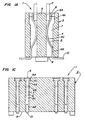
- FIG. 1A shows a cross sectional view of one preferred embodiment of a compact connector assembly according to the current invention.
- the assembly 1 comprises a pin 2 and a compact connector or receptacle 3.
- the compact connector 3 further comprises a side wall 4, an inner wall 5 and an electrically-conductive composite action beam 6.
- the composite action beam 6 is located in a bore 7 which is limited by the inner wall 5 and the sidewall 4.
- a movable or unsupported end 6A of the composite action beam 6 is located near a pin receiving opening 8 while a fixed or supported end 6B of the composite action beam 6 is located near a solder tail opening 9.
- a solder tail 10 of the composite action beam 6 is continuous with the composite action beam 6 at the fixed end 6B and protrudes through the solder tail opening 9.
- the solder tail 10 bends 90° around a bottom of the sidewall 4 and extends horizontally beyond the sidewall 4.
- the movable end 6A makes a contact with the pin 2 during an initial phase of an insertion cycle.
- the angle of attack by the pin 2 with respect to the movable end 6A may be relatively high during this initial phase, compared to later phases of the insertion cycle.
- the movable side 6A is located to one side of the pin receiving opening 8 during this phase of insertion.
- the center of arch 6C of the composite action beam 6 can abut against the inside wall 5.
- the pin-receiving opening 8 can be partially further indented on a surface 4A facing the movable end 6A.
- the deflection rate during the initial phase can be approximately 4 gram per mil according to a preferred embodiment of the current invention.
- the movable end 6A functions as a cantilever beam and requires low insertion force during this initial phase.
- FIG. 1B relative locations of the above discussed components in the compact connector according to the current invention are shown in a top view.
- the pin 2 In a pin-receiving opening 8, the pin 2 is shown in the most inner part against the inner wall 5.
- the pin 2 contacts the movable end 6A of the composite action beam 6 in an approximately center location of the pin receiving opening 8.
- Lateral to the movable end 6A is a space 7 and the fixed end 6B which abuts the sidewall 4.
- Further lateral to the sidewall 4 is a portion of the solder tail 10, which extends beyond the sidewall 4.
- there are eight pin-to-beam contacts on the connector there are eight pin-to-beam contacts on the connector. It is noted, however, that such a connector feature would most likely be applicable in high pin count configurations.
- Figure 1C shows another cross-sectional view of the miniature connector at 1C-1C of Figure 1B.
- the pin-receiving opening 8 has a larger diameter than the width of the composite action beam 6.
- the bore 7 indicated by a dotted line is limited by the inside walls of the connector 3.
- the composite action beam 6 shown in solid line has the movable end 6A near the pin-receiving opening 8, the arch portion 6C near the center of the bore 7 and the fixed end 6B near the solder tail opening 9.
- the solder tail 10 is contiguous with the fixed end 6B.
- the indented surface 4A further comprises a transition area 4B between the indented surface 4A and the inner surface of the side wall 4.
- the indented surface further comprises movable area 4C where a movement of the movable end 6A of the composite action beam 6 is accommodated.
- the movable end of the composite action beam 6 is guided within movable area 4C of the indented surface 4A so as to minimize the deviation from a predetermined course of movement.
- the width of the movable end 6A and the corresponding moveable area 4C is wider than the rest of the composite action beam 6 or the bore 7. This width differentiation prevents the moveable end 6A of the composite action beam from being pushed down towards the fixed end 6B so as to maintain its substantially horizontal movement near the pin-receiving opening 8 during the pin insertion cycle.
- solder tail opening 9 is filled. In such a construction it may not be necessary to provide movable end 6A with a portion that is wider than the composite action beam 6 or bore 7. Similarly, if movable end 6A is constructed as shown, it may not be necessary to fill solder tail opening 9.
- One advantage to filling solder tail opening 9 is the prevention of solder from flowing into bore 7 during mounting of the connector.
- Figure 2 illustrates an intermediate phase of the pin insertion cycle in a preferred embodiment according to the current invention as shown in Figure 1A.
- the pin is further inserted towards the center of the arch 6C of the composite action beam 6.
- the movable end 6A functions as a cantilever beam, and the movable end 6A moves towards the partially indented surface 4A of the sidewall 4.
- the partially indented surface 4A of the sidewall 4 can serve to narrow the overall width of the connector assembly 1.
- the movable end then abuts against the partially intended surface 4A as shown in Figure 2.
- the composite action beam 6 goes through a transition from a cantilever beam to a supported beam. Neither end of the composite action beam 6 no longer horizontally moves to accommodate further pin insertion.
- the center of the arch 6C deflects from this point on.
- the movable end 6A may move in the direction of an axis of insertion toward the pin receiving opening 8.
- the fixed end 6B of the composite action beam 6 remains stationary with respect to the sidewall 4. Accordingly, the deflection rate may increase up to approximately 16 grams per mil after the composite beam 6 acts as a two-point supported beam in a preferred embodiment of the current invention.
- the pin 2 has reached the final insertion point.
- the pin 2 is pressed against the inner wall 5 by the composite action beam 6 at a Hertzian stress dot 6D.
- the composite action beam 6 provides high normal force against the pin 2 relative to initial insertion force so as to retain the pin 2 in the final position.
- the composite action beam 6 now remains to function as a two-point supported beam.
- top 11 has been added to connector 1 which extends over pin receiving opening 8.
- the function of top 11 is to prevent stubbing of pins 2 on composite beam 6.
- the end portion of top 11 extending over pin receiving opening 8 is chamfered or tapered.
- Figures 1-3 illustrate a transition of the composite action beam 6 from a cantilever beam to a supported beam.
- Such a transition in the beam 6 yields low insertion force during an initial phase relative to high normal force against a completely inserted pin.
- Low insertion force is an advantage for a compact connector. Since the area required for each pin-to-beam contact is smaller with the composite action beam of the current invention, a larger number of the contacts may be placed in the compact connector. Thus, a total amount of insertion force needs to be kept minimal so as to make insertion relatively easy and reliable.
- the composite action beam of the current invention satisfies such a low insertion force requirement.
- the composite action beam of the current invention combines the advantageous features of the cantilever beam and the supported beam without sacrificing the space limitation of a compact connector.
- FIG. 4 Another embodiment of an electrical connector in accordance with the present invention is shown in Figs. 4 and 5.
- adjacent pin insertion openings 20 in the connector housing 22 are closely spaced together, both in the longitudinal and lateral direction.
- a counter-sink bore 24 of each pin insertion opening 20 is in communication with an insertion bore 26 such that the counter-sink bore facilitates easy insertion of adjacent pins 28 into the insertion bores 26 of laterally adjacent pin insertion openings 20.
- Pin 28 and the counter-sink bore 24 and insertion bore 26 all have a coincidental central axis 30 such that the pins 28 are inserted into the openings 20 along the central axis 30.
- the insertion bores 26 are only slightly larger than, and preferably the same shape as, the external surface of the pins 28, taking into account the necessary tolerances of the structure.
- each opening 20 is in communication with a spring retention bore 32 in the housing, with the central axis of the spring retention bore being parallel to, but displaced from, the axis of insertion of the pins along central axis 30.
- a surface 34 of the insertion bore 26 is substantially aligned with a surface 36 of the spring retention bore 32 such that the pins 28 are inserted into the spring retention bore closely adjacent to, and preferably contacting, the surface 36 of the spring retention bore 32.
- the pins 28 are thus inserted into contact with the contact beams 38 in the manner described above such that the pins are retained against the surface 36. In this manner, the tolerances of the assembly can be low, while ensuring that the pins contact a wall of the housing when the contact beam applies a high normal force in order to retain the pins in the housing.
- the connector housing 22 has a cavity 40 in the bottom surface 41.
- the contact beams 38 are mounted in a receptacle 42 such that the contact beams are detachably mounted within the housing when the receptacle 42 is mounted into the cavity 40.
- one row of contact beams is disposed in one half of a receptacle 42.
- each half of the receptacle 42 includes alternating pins 44 and holes 46, which are preferably square.
- these rows of contact beams are easily manufactured separately and subsequently assembled together with the pins of one row connected into a corresponding hole of another row in a known manner to form a single receptacle having adjacent rows of contact beams. Accordingly, the rows of adjacent contact beams are inserted into the spring retention bore and detentes 48 on the receptacle 42 engage the walls 50 of the connector housing, causing elastic deformation of the walls in the area of the detentes, such that the receptacle is mechanically connected to the connector housing.
- connector housing 22 in order to facilitate insertion of the contact beam rows into the housing, in a preferred embodiment connector housing 22 includes beam insertion ramps 52. These ramps comprise a flat portion 54, extending from the base of the insertion bore, and a sloped portion 56 which extends toward the bottom surface 41 of the connector housing. Upon insertion of the contact beams in the spring retention bore, the contact beams slide up the sloped portion 54 and onto the flat portion 56 such that all of the insertion tolerances are applied to one side of the connector housing and can be accounted for during manufacture of the connector structure.
- a preferred embodiment of a contact beam 38 is shown in Fig. 7b.
- a straight portion 60 is disposed within the receptacle 42.
- the straight portion 60 is molded into the receptacle during the manufacture of the beam and receptacle assembly such that solder used to mount the contact beam to a printed substrate cannot flow from the bottom of the connector housing and into the spring retention bore.
- Another straight portion 62 extends at an angle from one end of the straight portion 60.
- the straight portion 62 is joined to a curved contact portion 64 and the curved contact portion 64 is joined to top portion 66.
- the end of the contact beam including the straight portion 60 and curved contact portion 64 is the end that is inserted into the spring retention bore, as shown in Fig. 5.
- the pins 28 when the pins 28 are inserted into the openings 20 of the housing 22 they contact the curved contact portion 64 of the contact beam 38 and the top portion 66 of the beam deflects away from the surface 36.
- the curved contact portion of the contact beam applies a high normal force against the pins for retaining the pins in the housing in the manner described above.
- mounting portion 68 of the contact beam extends from the other end of straight portion 60.
- mounting portion 68 is for straddle mounting of the connector wherein the mounting portion of the contact beam in the adjacent rows of beams is soldered to a pad on either side of a printed circuit board or the like in a known manner.
- the present invention is not intended to be limited in this manner and a known mounting portion for surface mounting the connector is within the scope of the invention.
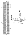
- a terminal pin header 80 for mating with connector housing 22 is shown in Fig. 8.
- Electrical connection is established between a plurality of terminal pins 82 disposed in the header 80 and the contact beams 38 disposed in connector housing 22.
- Header 80 is a right angle header wherein the terminal pins 82 are bent substantially at right angles within the header in the manner set forth in further detail below.
- the circuit board end 84 of the terminal pins is inserted into holes 85 in a printed circuit board 86 and solderably connected thereto in a known manner for establishing electrical connection between the printed circuitry (not shown) on the circuit board and the contact beams 38. Accordingly, the mounting portion 68 of the contact beams 38 can be connected to a second printed circuit board or the like such that an electrical connection is established between the first and second printed circuit boards for carrying out a variety of functions in a known manner.
- the terminal pins 82 are disposed in header housing 88 and stand-off pin guide 90, wherein pin guide 90 is bolted to header housing 88 by bolts 91.
- pin guide 90 is bolted to header housing 88 by bolts 91.
- eight longitudinal rows of terminal pins 82 are disposed in the pin header 80.
- two adjacent header housings 88 are mated together.
- the present invention is not intended to be limited in this manner, and any number of longitudinal rows of pins can be provided, depending upon the application requirements.
- four longitudinal rows of terminal pins are provided with only one header housing 88.
- the pins are aligned in two adjacent rows per each header housing 88.
- the number and arrangement of the terminal pin rows at the circuit board end 84 of the pins 82 can be configured to meet the desired mating requirements for the printed circuit board.
- the pins are bent substantially at a right angle 93 with the pins in one vertical column being bent in an upward direction and the pins in an adjacent vertical column being bent in a downward direction.
- the connector housing is inserted into the cavity 94 in the header housing 188.
- two separate connector housings 22 are mated with the header.
- the connector end 92 of the two adjacent rows of terminal pins is inserted into the corresponding adjacent rows of pin insertion openings 20 such that the pins contact the contact beams 38 in the manner described above.
- the pins are simply inserted into the connector housing 22 without interference such as pin stubbing.
- a longitudinal row 98 of terminal pins 82 is molded into a top retention and alignment wafer 100 and a bottom retention and alignment wafer 102, the wafers 100 and 102 comprising a molded plastic material.
- the terminal pins are aligned in a die and the molded wafers are formed out of molten plastic material with projections 104 and sockets 106 being formed as part of the wafers.
- projections in the mold form the sockets 106. The projections on the mold extend into contact with and positively locate the row of pins, i.e.
- sockets 106 extend into contact with the pins, such that alignment of the pins can be measured and maintained within a desired tolerance.
- the pins can be embossed to form a bulge 107 such that the bulge is used to positively secure the row of pins in the header housing when the pins are inserted therein in the manner set forth below.
- Figs. 10 and 11 after the individual longitudinal rows of pins are bent substantially at a right angle and adjacent rows of pins are joined by connecting wafers 100, 102, the top wafers 100 are inserted into wafer cavity 110 in each of the header housings 88. Projections 104 of the wafer 100 are supported upon shoulder 112 of the housing and the connector end 92 of the pins extends through adjacent pin holes 113 in the header housing 88. Countersinks 114 in the pin holes 113 assist in the positive location of the pins in the pin holes and obviate pin stubbing.
- adjacent rows of pins are properly aligned within the header housing such that the desired tolerances of the connector components are maintained and the header can be simply mated with the connector housing such that the pins are effectively connected to the contact beams in the connector housing in the manner set forth above.
- stand-off pin guide 90 in order to provide for proper alignment, within a desired tolerance, of the circuit board end 84 of the pins when the pins are connected to the printed circuit board 86, stand-off pin guide 90 includes a plurality of longitudinal rows of pin guide holes 120. In the embodiment shown in Fig. 13a, eight longitudinal rows of pin guide holes are provided for receiving eight rows of terminal pins discussed above. It should be noted that the rear surface 122 of the pin guide is mounted to the header housing 88 with the bolts 91 extending through bolt holes 123.
- ridges in the pin guide form four inclined ramp surfaces 124, 125, 126, 127 around each of the holes 120 wherein the ramp surfaces extend into communication with the holes 120. Accordingly, the pins are positively inserted into the pin guide 90 along the ramp surfaces and into the holes 120. Thus, pin stubbing is obviated and the ridges ensure that the pins are properly guided into the pin guide holes.
- the present invention provides for connection of a large array of pins to a printed circuit board such that all of the pins are properly aligned and thus, can be simply inserted into their respective holes on the board.
Claims (23)
- Connecteur électrique comprenant :un logement de broches (88) ; etdeux ou plusieurs rangées (98) d'inserts de broches de bornes, disposées dans ledit logement de broches, chacune desdites rangées d'inserts de broches de bornes comprenant :une pluralité de broches de bornes (82) ayant des première et deuxième extrémités, lesdites broches de bornes étant disposées dans une première plaquette de connexion (100) positionnée de façon proximale à ladite première extrémité; caractérisé en ce que les broches de bornes sont également disposées dans une deuxième plaquette (102) positionnée de façon proximale à ladite deuxième extrémité et en ce que chaque plaquette de connexion possède des surfaces latérales, une pluralité de projections (104), s'étendant depuis au moins une desdites surfaces latérales, et une pluralité de supports (106) s'étendant dans au moins une desdites surfaces latérales, dans lequel ladite première rangée d'inserts de broches de bornes est connectée à ladite deuxième rangée d'inserts de broches de bornes en insérant lesdites projections de ladite première plaquette de connexion (100) de ladite première rangée d'inserts de broches de bornes dans lesdits supports de ladite première plaquette de connexion de ladite deuxième rangée d'inserts de broches de bornes et, en outre, en insérant lesdites projections de ladite deuxième plaquette de connexion (102) de ladite première rangée d'inserts de broches de bornes dans lesdits supports de ladite deuxième plaquette de connexion de ladite deuxième rangée d'inserts de broches de bornes.
- Connecteur électrique selon la revendication 1, dans lequel ledit logement de bornes possède une première et une deuxième cavité (110, 94), la première plaquette de connexion (100) de chacune desdites première et deuxième rangées d'inserts de broches de bornes étant disposée dans ladite première cavité (110) et ladite première extrémité desdites broches de bornes de chacune desdites première et deuxième rangées d'inserts de broches de bornes s'étendant dans ladite deuxième cavité (94).
- Connecteur électrique selon la revendication 1, dans lequel chacune desdites broches de bornes (82) possède une surface de broches (107) et lesdits supports s'étendent depuis une surface latérale jusqu'au contact avec ladite surface de broche.
- Connecteur électrique selon une quelconque des revendications 1 à 3 et, en outre, comprenant un guide de broches (90) ayant une ou plusieurs rangées de trous de broches (120) s'étendant à travers ledit guide de broches afin de recevoir ladite deuxième extrémité desdites broches de bornes, ledit guide de broches ayant, en outre, des nervures formant quatre surfaces en rampe inclinée (124 à 129) sur le pourtour de chacun desdits trous de broches et s'étendant en communication avec chacun desdits trous de broches.
- Connecteur électrique selon une quelconque des revendications 1 à 4, dans lequel lesdites broches de bornes (82) sont courbées sensiblement selon un angle droit entre lesdites première et deuxième plaquettes de connexion (100, 102).
- Connecteur électrique selon une quelconque des revendications 1 à 4, dans lequel ladite deuxième extrémité de chacune desdites broches de bornes (82) est courbée sensiblement selon un angle droit dans une première direction, puis est, en outre, courbée sensiblement selon un angle droit dans une deuxième direction, ladite première direction étant sensiblement normale à ladite deuxième direction.
- Connecteur électrique selon une quelconque des revendications 1 à 6, dans lequel le logement de broches (88) possède une première et une deuxième surfaces et les broches de bornes (82) s'étendent en rangées à partir des première et deuxième surfaces, le nombre de rangées d'extrémité de broches s'étendant à partir de la première surface étant le double du nombre de rangées d'extrémité de broches s'étendant à partir de la deuxième surface.
- Connecteur électrique selon la revendication 7, dans lequel au moins deux des broches de bornes (82) qui s'étendent à partir de la première surface ont des longueurs sensiblement égales.
- Connecteur électrique selon la revendication 7, dans lequel les premières extrémités des broches de bornes (82) ont des longueurs sensiblement égales.
- Ensemble de connecteur électrique composé d'un connecteur électrique selon la revendication 2 ou une quelconque des revendications 3 à 6 lorsqu'elles se rapportent à la revendication 2, en combinaison avec un deuxième connecteur comprenant un logement de contacts (22) ayant deux ou davantage de rangées d'alésages d'insertion (7, 32), dont le nombre correspond au nombre de rangées d'inserts de broches de bornes, et une pluralité de lames de contact (6, 38) disposées dans ledit logement de manière à ce que chaque lame de contact soit accessible par un alésage correspondant desdits alésages d'insertion, grâce à quoi ledit logement de contacts (22) est disposé dans ladite deuxième cavité (94) dudit logement de broches (88) de telle sorte que ladite première extrémité de chacune des broches de bornes soit insérée dans un alésage correspondant desdits alésages d'insertion et vienne au contact de la lame de contact associée.
- Ensemble de connecteur électrique selon la revendication 10, dans lequel chacune desdites lames de contact possède une première et une deuxième extrémités (6A, 6B), la première extrémité (6B) étant supportée dans le logement de contacts et la deuxième extrémité (6A) venant au contact de la broche de bornes associée (82).
- Ensemble de connecteur électrique selon la revendication 11, dans lequel les deuxièmes extrémités (6A) des lames de contact sont libres et non supportées lorsque les broches de bornes (82) ne sont pas insérées, de sorte que les lames fonctionnent en porte à faux et chaque lame occasionne un taux de fléchissement sensiblement faible, au cours d'un déplacement d'une phase initiale d'insertion, de ladite extrémité non supportée vers une paroi intérieure (45, 36) du logement, provoqué par une insertion de la broche de borne associée dans l'alésage d'insertion associé (7, 32) jusqu'à ce que ladite extrémité non supportée atteigne ladite paroi intérieure et vienne en glissant au contact de ladite paroi intérieure au cours d'une phase ultérieure d'insertion de la broche de bornes associée, afin de devenir une lame supportée ayant une extrémité non contrainte au cours de ladite phase ultérieure, de manière à exercer une force normale sensiblement importante sur la broche, tout en procurant une force d'insertion relativement faible.
- Ensemble de connecteur électrique selon la revendication 12, dans lequel le logement possède un certain nombre de parois intérieures (4, 5, 36), une desdites parois intérieures ayant une surface partiellement en retrait (4A) fournissant un espace additionnel pour ladite extrémité non supportée de la lame associée sans accroítre la largeur extérieure dudit logement de contacts.
- Ensemble de connecteur électrique selon la revendication 12, dans lequel ladite paroi intérieure possède une surface partiellement en retrait (4A) et ladite extrémité non supportée (6) de la lame associée vient en glissant au contact de ladite surface partiellement en retrait de manière à fournir un espace additionnel pour un déplacement de ladite extrémité non supportée sans accroítre la largeur extérieure dudit logement de contacts.
- Ensemble de connecteur électrique selon la revendication 12, dans lequel ladite paroi intérieure est sensiblement lisse sur la longueur du déplacement glissant de l'extrémité libre de la lame associée sur celle-ci.
- Ensemble de connecteur électrique selon une quelconque des revendications 12 à 15, dans lequel chaque lame de contact possède un taux de fléchissement d'approximativement 4 grammes par millième de pouce au cours de ladite phase initiale.
- Ensemble de connecteur électrique selon une quelconque des revendications 12 à 16, dans lequel chaque lame de contact possède un taux de fléchissement de jusqu'à approximativement 16 grammes par millième de pouce au cours de ladite phase ultérieure.
- Ensemble de connecteur électrique selon une quelconque des revendications 12 à 17, dans lequel ladite deuxième extrémité de chaque lame de contact est dotée d'une surface de contact ayant un certain rayon pour glisser le long de ladite paroi intérieure.
- Ensemble de connecteur électrique selon la revendication 12, dans lequel chaque lame (38) comprend une première partie (62), une deuxième partie (60), une partie de montage (68) et une partie de contact (64), toutes intégrales les unes aux autres, ladite deuxième partie (60) étant disposée à l'intérieur dudit logement de contacts et ladite première partie (62) s'étendant en formant un angle par rapport à ladite deuxième partie et à l'intérieur dudit alésage d'insertion, ladite partie de contact servant à venir au contact de la broche associée (82) afin de retenir ladite broche contre une surface de la paroi intérieure et ladite partie de montage (68) étant jointe de façon intégrale à une deuxième extrémité de ladite deuxième partie et s'étendant à l'extérieur dudit logement pour une connexion électrique avec un conducteur.
- Ensemble de connecteur électrique selon la revendication 19, dans lequel ladite deuxième partie (60) est moulée à l'intérieur dudit logement de contacts.
- Ensemble de connecteur électrique selon une quelconque des revendications 10 à 20, dans lequel ledit logement de contacts possède une surface extérieure avec des alésages fraisés (24) en communication avec lesdits alésages d'insertion (26).
- Ensemble de connecteur électrique selon une quelconque des revendications 10 à 21, dans lequel ledit logement de contacts comprend, en outre, des rampes de chargement de lames (52), chacune comprenant une partie de surface s'étendant à partir d'un desdits alésages d'insertion et une partie s'étendant vers une surface extérieure du logement de contact afin de faciliter l'insertion d'une desdites lames de contacts dans ledit alésage d'insertion.
- Ensemble de connecteur électrique selon une quelconque des revendications 10 à 22, dans lequel existe un alésage de retenue de lame (32) dans le logement (22), en communication avec chaque alésage d'insertion (26) et recevant la lame de contact associée (6, 38), l'axe de l'alésage de retenue de lame (32) étant espacé et parallèle à l'axe de l'alésage d'insertion (26).
Applications Claiming Priority (7)
| Application Number | Priority Date | Filing Date | Title |
|---|---|---|---|
| US19344394A | 1994-02-08 | 1994-02-08 | |
| US193443 | 1994-02-08 | ||
| US22107794A | 1994-03-31 | 1994-03-31 | |
| US221077 | 1994-03-31 | ||
| US235289 | 1994-04-29 | ||
| US08/235,289 US5511984A (en) | 1994-02-08 | 1994-04-29 | Electrical connector |
| PCT/US1995/001465 WO1995022182A1 (fr) | 1994-02-08 | 1995-02-06 | Connecteur electrique |
Publications (3)
| Publication Number | Publication Date |
|---|---|
| EP0801821A4 EP0801821A4 (fr) | 1997-10-22 |
| EP0801821A1 EP0801821A1 (fr) | 1997-10-22 |
| EP0801821B1 true EP0801821B1 (fr) | 2003-06-25 |
Family
ID=27393198
Family Applications (1)
| Application Number | Title | Priority Date | Filing Date |
|---|---|---|---|
| EP95910176A Expired - Lifetime EP0801821B1 (fr) | 1994-02-08 | 1995-02-06 | Connecteur electrique |
Country Status (6)
| Country | Link |
|---|---|
| US (1) | US5713746A (fr) |
| EP (1) | EP0801821B1 (fr) |
| JP (1) | JPH09508749A (fr) |
| DE (1) | DE69531165T2 (fr) |
| SG (2) | SG85669A1 (fr) |
| WO (1) | WO1995022182A1 (fr) |
Cited By (2)
| Publication number | Priority date | Publication date | Assignee | Title |
|---|---|---|---|---|
| CN102623824A (zh) * | 2011-01-31 | 2012-08-01 | 安费诺公司 | 多阶段梁型触头 |
| CN104347988A (zh) * | 2013-08-02 | 2015-02-11 | 安费诺公司 | 多级梁型触头 |
Families Citing this family (51)
| Publication number | Priority date | Publication date | Assignee | Title |
|---|---|---|---|---|
| JPH11111405A (ja) * | 1997-10-03 | 1999-04-23 | Japan Aviation Electron Ind Ltd | 基板実装用コネクタ |
| US5980272A (en) * | 1997-10-21 | 1999-11-09 | Hon Hai Precision Ind. Co., Ltd. | Electrical connector with back shell for contact tails |
| US6093032A (en) * | 1997-10-22 | 2000-07-25 | Mchugh; Robert G. | Connector with spacer |
| JP2001143808A (ja) * | 1999-11-17 | 2001-05-25 | Mitsumi Electric Co Ltd | 電源プラグ機構 |
| US6869292B2 (en) * | 2001-07-31 | 2005-03-22 | Fci Americas Technology, Inc. | Modular mezzanine connector |
| US7390200B2 (en) * | 2001-11-14 | 2008-06-24 | Fci Americas Technology, Inc. | High speed differential transmission structures without grounds |
| US6981883B2 (en) * | 2001-11-14 | 2006-01-03 | Fci Americas Technology, Inc. | Impedance control in electrical connectors |
| CN100483886C (zh) * | 2001-11-14 | 2009-04-29 | Fci公司 | 用于电连接器的串扰减小 |
| US20050170700A1 (en) * | 2001-11-14 | 2005-08-04 | Shuey Joseph B. | High speed electrical connector without ground contacts |
| US6994569B2 (en) * | 2001-11-14 | 2006-02-07 | Fci America Technology, Inc. | Electrical connectors having contacts that may be selectively designated as either signal or ground contacts |
| US20050196987A1 (en) * | 2001-11-14 | 2005-09-08 | Shuey Joseph B. | High density, low noise, high speed mezzanine connector |
| US6837720B2 (en) | 2001-11-27 | 2005-01-04 | Sun Microsystems, Inc. | Connector for electrically coupling one or more devices in a processor-based system |
| US6793507B2 (en) * | 2002-12-13 | 2004-09-21 | Hewlett-Packard Development Company, L.P. | Cable connector riser |
| TW568458U (en) * | 2003-05-23 | 2003-12-21 | Hon Hai Prec Ind Co Ltd | Electrical connector |
| US6997750B2 (en) * | 2003-07-23 | 2006-02-14 | Fci Americas Technology, Inc. | Electrical connector contact |
| US7517250B2 (en) | 2003-09-26 | 2009-04-14 | Fci Americas Technology, Inc. | Impedance mating interface for electrical connectors |
| US7524209B2 (en) * | 2003-09-26 | 2009-04-28 | Fci Americas Technology, Inc. | Impedance mating interface for electrical connectors |
| DE102004027712B4 (de) * | 2004-06-07 | 2007-09-06 | Tyco Electronics Amp Gmbh | Kontaktanordnung für Leiterplatten |
| US7281950B2 (en) * | 2004-09-29 | 2007-10-16 | Fci Americas Technology, Inc. | High speed connectors that minimize signal skew and crosstalk |
| US20060228912A1 (en) * | 2005-04-07 | 2006-10-12 | Fci Americas Technology, Inc. | Orthogonal backplane connector |
| US20060245137A1 (en) * | 2005-04-29 | 2006-11-02 | Fci Americas Technology, Inc. | Backplane connectors |
| US7462924B2 (en) * | 2006-06-27 | 2008-12-09 | Fci Americas Technology, Inc. | Electrical connector with elongated ground contacts |
| US7201587B1 (en) * | 2006-07-31 | 2007-04-10 | Delphi Technologies, Inc. | Electrical connector with right angle terminal pins |
| US7500871B2 (en) * | 2006-08-21 | 2009-03-10 | Fci Americas Technology, Inc. | Electrical connector system with jogged contact tails |
| US7713088B2 (en) | 2006-10-05 | 2010-05-11 | Fci | Broadside-coupled signal pair configurations for electrical connectors |
| CN200972950Y (zh) * | 2006-10-09 | 2007-11-07 | 富士康(昆山)电脑接插件有限公司 | 电连接器 |
| US7708569B2 (en) | 2006-10-30 | 2010-05-04 | Fci Americas Technology, Inc. | Broadside-coupled signal pair configurations for electrical connectors |
| US7497736B2 (en) | 2006-12-19 | 2009-03-03 | Fci Americas Technology, Inc. | Shieldless, high-speed, low-cross-talk electrical connector |
| US7811100B2 (en) * | 2007-07-13 | 2010-10-12 | Fci Americas Technology, Inc. | Electrical connector system having a continuous ground at the mating interface thereof |
| US8764464B2 (en) * | 2008-02-29 | 2014-07-01 | Fci Americas Technology Llc | Cross talk reduction for high speed electrical connectors |
| CN102282731B (zh) | 2008-11-14 | 2015-10-21 | 莫列斯公司 | 共振修正连接器 |
| CN102318143B (zh) | 2008-12-12 | 2015-03-11 | 莫列斯公司 | 谐振调整连接器 |
| US9277649B2 (en) | 2009-02-26 | 2016-03-01 | Fci Americas Technology Llc | Cross talk reduction for high-speed electrical connectors |
| US8366485B2 (en) | 2009-03-19 | 2013-02-05 | Fci Americas Technology Llc | Electrical connector having ribbed ground plate |
| US8608510B2 (en) * | 2009-07-24 | 2013-12-17 | Fci Americas Technology Llc | Dual impedance electrical connector |
| US8267721B2 (en) * | 2009-10-28 | 2012-09-18 | Fci Americas Technology Llc | Electrical connector having ground plates and ground coupling bar |
| US8616919B2 (en) * | 2009-11-13 | 2013-12-31 | Fci Americas Technology Llc | Attachment system for electrical connector |
| CN102725919B (zh) * | 2009-12-30 | 2015-07-08 | Fci公司 | 具有阻抗调节肋的电连接器 |
| US9136634B2 (en) | 2010-09-03 | 2015-09-15 | Fci Americas Technology Llc | Low-cross-talk electrical connector |
| US10243284B2 (en) | 2011-01-31 | 2019-03-26 | Amphenol Corporation | Multi-stage beam contacts |
| KR101314105B1 (ko) * | 2011-10-12 | 2013-10-04 | 주식회사 유라코퍼레이션 | 자동변속기용 하네스 |
| EP2624034A1 (fr) | 2012-01-31 | 2013-08-07 | Fci | Dispositif de couplage optique démontable |
| USD727268S1 (en) | 2012-04-13 | 2015-04-21 | Fci Americas Technology Llc | Vertical electrical connector |
| USD727852S1 (en) | 2012-04-13 | 2015-04-28 | Fci Americas Technology Llc | Ground shield for a right angle electrical connector |
| US8944831B2 (en) | 2012-04-13 | 2015-02-03 | Fci Americas Technology Llc | Electrical connector having ribbed ground plate with engagement members |
| US9257778B2 (en) | 2012-04-13 | 2016-02-09 | Fci Americas Technology | High speed electrical connector |
| USD718253S1 (en) | 2012-04-13 | 2014-11-25 | Fci Americas Technology Llc | Electrical cable connector |
| US9543703B2 (en) | 2012-07-11 | 2017-01-10 | Fci Americas Technology Llc | Electrical connector with reduced stack height |
| USD751507S1 (en) | 2012-07-11 | 2016-03-15 | Fci Americas Technology Llc | Electrical connector |
| USD745852S1 (en) | 2013-01-25 | 2015-12-22 | Fci Americas Technology Llc | Electrical connector |
| USD720698S1 (en) | 2013-03-15 | 2015-01-06 | Fci Americas Technology Llc | Electrical cable connector |
Family Cites Families (17)
| Publication number | Priority date | Publication date | Assignee | Title |
|---|---|---|---|---|
| GB879968A (en) * | 1958-01-20 | 1961-10-11 | Siemens Ag | Improvements relating to electrical plug and socket connectors |
| US4036544A (en) * | 1974-10-16 | 1977-07-19 | Bunker Ramo Corporation | Contact for multiple conductor connector |
| US3963317A (en) * | 1975-04-03 | 1976-06-15 | E. I. Du Pont De Nemours And Company | Zero force edge connector block |
| US4420215A (en) * | 1979-12-26 | 1983-12-13 | A P Products Incorporated | Variable effective length cantilever contact and connector |
| US4775333A (en) * | 1985-12-23 | 1988-10-04 | Ford Motor Company | Method of assembling an improved electrical connector |
| DE8713932U1 (fr) * | 1987-10-16 | 1988-01-14 | Du Pont De Nemours (Nederland) B.V., Dordrecht, Nl | |
| US4846734A (en) * | 1988-01-22 | 1989-07-11 | Burndy Corporation | Vertical edge card connectors |
| DE69018000T2 (de) * | 1989-10-10 | 1995-09-28 | Whitaker Corp | Rückwandsteckverbinder mit angepasster Impedanz. |
| US5197893A (en) * | 1990-03-14 | 1993-03-30 | Burndy Corporation | Connector assembly for printed circuit boards |
| US5133679A (en) * | 1990-06-08 | 1992-07-28 | E. I. Du Pont De Nemours And Company | Connectors with ground structure |
| JPH074782Y2 (ja) * | 1990-09-17 | 1995-02-01 | ヒロセ電機株式会社 | 電気コネクタ構造 |
| US5074039A (en) * | 1990-10-26 | 1991-12-24 | Amp Incorporated | Method of manufacturing electrical connectors |
| US5236368A (en) * | 1992-01-06 | 1993-08-17 | Burndy Corporation | Printed circuit board and outrigger edge connector assembly and method of assembling the same |
| JP2570939Y2 (ja) * | 1992-03-26 | 1998-05-13 | 日本エー・エム・ピー株式会社 | シールド型電気コネクタ及びそれに使用する固定金具 |
| US5273461A (en) * | 1992-08-28 | 1993-12-28 | Lee Chih Ta | Electronic connector for electrically connecting an electronic module to a printed circuit board |
| US5387114A (en) * | 1993-07-22 | 1995-02-07 | Molex Incorporated | Electrical connector with means for altering circuit characteristics |
| US5413491A (en) * | 1993-10-13 | 1995-05-09 | Burndy Corporation | Small form factor connectors with center ground plate |
-
1995
- 1995-02-06 JP JP7521274A patent/JPH09508749A/ja active Pending
- 1995-02-06 SG SG9903980A patent/SG85669A1/en unknown
- 1995-02-06 SG SG1996002802A patent/SG50495A1/en unknown
- 1995-02-06 DE DE69531165T patent/DE69531165T2/de not_active Expired - Lifetime
- 1995-02-06 EP EP95910176A patent/EP0801821B1/fr not_active Expired - Lifetime
- 1995-02-06 WO PCT/US1995/001465 patent/WO1995022182A1/fr active IP Right Grant
-
1996
- 1996-04-30 US US08/643,072 patent/US5713746A/en not_active Expired - Lifetime
Cited By (5)
| Publication number | Priority date | Publication date | Assignee | Title |
|---|---|---|---|---|
| CN102623824A (zh) * | 2011-01-31 | 2012-08-01 | 安费诺公司 | 多阶段梁型触头 |
| CN102623824B (zh) * | 2011-01-31 | 2016-12-14 | 安费诺公司 | 多阶段梁型触头 |
| CN107425328A (zh) * | 2011-01-31 | 2017-12-01 | 安费诺公司 | 多阶段梁型触头 |
| CN104347988A (zh) * | 2013-08-02 | 2015-02-11 | 安费诺公司 | 多级梁型触头 |
| CN104347988B (zh) * | 2013-08-02 | 2018-09-25 | 安费诺公司 | 多级梁型触头 |
Also Published As
| Publication number | Publication date |
|---|---|
| US5713746A (en) | 1998-02-03 |
| DE69531165T2 (de) | 2004-04-08 |
| WO1995022182A1 (fr) | 1995-08-17 |
| DE69531165D1 (de) | 2003-07-31 |
| SG50495A1 (en) | 1998-07-20 |
| JPH09508749A (ja) | 1997-09-02 |
| EP0801821A4 (fr) | 1997-10-22 |
| SG85669A1 (en) | 2002-01-15 |
| EP0801821A1 (fr) | 1997-10-22 |
Similar Documents
| Publication | Publication Date | Title |
|---|---|---|
| EP0801821B1 (fr) | Connecteur electrique | |
| US5511984A (en) | Electrical connector | |
| US6902411B2 (en) | Connector assembly | |
| US7270573B2 (en) | Electrical connector with load bearing features | |
| US5876217A (en) | Electric connector assembly with improved retention characteristics | |
| US9577379B2 (en) | Connector | |
| US5921787A (en) | Board-to-board interconnection | |
| JP4782740B2 (ja) | 低背コネクタ | |
| US5902136A (en) | Electrical connector for use in miniaturized, high density, and high pin count applications and method of manufacture | |
| US7381071B2 (en) | Floating electrical connector with twisted contacts | |
| EP1535310A2 (fr) | Connecteur electrique constitue d'un ensemble de contact a noyau | |
| US4722700A (en) | Low insertion force terminal for use with circuit panel | |
| US6079988A (en) | Electrical connector having spring contact with double contact projections as a contact region with contact pad of an external electronic component | |
| EP1128477B1 (fr) | Connecteur électrique avec contacts à compression | |
| US4725250A (en) | High density circuit panel socket | |
| US6336823B2 (en) | Electrical connector having female contact preload section | |
| US6132258A (en) | Board to board electrical connector | |
| US6450824B1 (en) | Connector including movable cover | |
| US6077092A (en) | Electrical connector having stabilizing structure for spacer and terminal | |
| US5921788A (en) | Electrical header with improved post retention | |
| EP0299989B1 (fr) | Prise pour plaquette de circuit a haute densite | |
| US20230146943A1 (en) | Pin array assembly and connector for high-speed signal transmission using the same | |
| JP3294634B2 (ja) | 電気コネクタ | |
| US20230223715A1 (en) | Connector for high-speed signal transmission with rigid alignment function | |
| CN215184887U (zh) | 基板连接用插头连接器 |
Legal Events
| Date | Code | Title | Description |
|---|---|---|---|
| PUAI | Public reference made under article 153(3) epc to a published international application that has entered the european phase |
Free format text: ORIGINAL CODE: 0009012 |
|
| 17P | Request for examination filed |
Effective date: 19960907 |
|
| A4 | Supplementary search report drawn up and despatched |
Effective date: 19970630 |
|
| AK | Designated contracting states |
Kind code of ref document: A4 Designated state(s): DE FR GB Kind code of ref document: A1 Designated state(s): DE FR GB |
|
| RAP1 | Party data changed (applicant data changed or rights of an application transferred) |
Owner name: BERG ELECTRONICS MANUFACTURING B.V. |
|
| 17Q | First examination report despatched |
Effective date: 19991111 |
|
| GRAG | Despatch of communication of intention to grant |
Free format text: ORIGINAL CODE: EPIDOS AGRA |
|
| GRAG | Despatch of communication of intention to grant |
Free format text: ORIGINAL CODE: EPIDOS AGRA |
|
| GRAH | Despatch of communication of intention to grant a patent |
Free format text: ORIGINAL CODE: EPIDOS IGRA |
|
| RAP1 | Party data changed (applicant data changed or rights of an application transferred) |
Owner name: FCI |
|
| GRAH | Despatch of communication of intention to grant a patent |
Free format text: ORIGINAL CODE: EPIDOS IGRA |
|
| GRAA | (expected) grant |
Free format text: ORIGINAL CODE: 0009210 |
|
| AK | Designated contracting states |
Designated state(s): DE FR GB |
|
| REG | Reference to a national code |
Ref country code: GB Ref legal event code: FG4D |
|
| RIC1 | Information provided on ipc code assigned before grant |
Ipc: 7H 01R 12/20 B Ipc: 7H 01R 12/18 B Ipc: 7H 01R 13/193 B Ipc: 7H 01R 12/32 B Ipc: 7H 01R 12/04 A |
|
| REF | Corresponds to: |
Ref document number: 69531165 Country of ref document: DE Date of ref document: 20030731 Kind code of ref document: P |
|
| ET | Fr: translation filed | ||
| PLBE | No opposition filed within time limit |
Free format text: ORIGINAL CODE: 0009261 |
|
| STAA | Information on the status of an ep patent application or granted ep patent |
Free format text: STATUS: NO OPPOSITION FILED WITHIN TIME LIMIT |
|
| 26N | No opposition filed |
Effective date: 20040326 |
|
| REG | Reference to a national code |
Ref country code: FR Ref legal event code: CA |
|
| PGFP | Annual fee paid to national office [announced via postgrant information from national office to epo] |
Ref country code: FR Payment date: 20120203 Year of fee payment: 18 |
|
| PGFP | Annual fee paid to national office [announced via postgrant information from national office to epo] |
Ref country code: DE Payment date: 20120229 Year of fee payment: 18 |
|
| REG | Reference to a national code |
Ref country code: DE Ref legal event code: R082 Ref document number: 69531165 Country of ref document: DE Representative=s name: BEETZ & PARTNER PATENT- UND RECHTSANWAELTE, DE Effective date: 20120419 Ref country code: DE Ref legal event code: R081 Ref document number: 69531165 Country of ref document: DE Owner name: FCI, FR Free format text: FORMER OWNER: FCI, PARIS, FR Effective date: 20120419 |
|
| PGFP | Annual fee paid to national office [announced via postgrant information from national office to epo] |
Ref country code: GB Payment date: 20120127 Year of fee payment: 18 |
|
| GBPC | Gb: european patent ceased through non-payment of renewal fee |
Effective date: 20130206 |
|
| REG | Reference to a national code |
Ref country code: FR Ref legal event code: ST Effective date: 20131031 |
|
| REG | Reference to a national code |
Ref country code: DE Ref legal event code: R119 Ref document number: 69531165 Country of ref document: DE Effective date: 20130903 |
|
| PG25 | Lapsed in a contracting state [announced via postgrant information from national office to epo] |
Ref country code: GB Free format text: LAPSE BECAUSE OF NON-PAYMENT OF DUE FEES Effective date: 20130206 Ref country code: FR Free format text: LAPSE BECAUSE OF NON-PAYMENT OF DUE FEES Effective date: 20130228 Ref country code: DE Free format text: LAPSE BECAUSE OF NON-PAYMENT OF DUE FEES Effective date: 20130903 |