EP0801148B1 - Verfahren und Vorrichtung zum Herstellen von Siliciumschichten - Google Patents
Verfahren und Vorrichtung zum Herstellen von Siliciumschichten Download PDFInfo
- Publication number
- EP0801148B1 EP0801148B1 EP97302514A EP97302514A EP0801148B1 EP 0801148 B1 EP0801148 B1 EP 0801148B1 EP 97302514 A EP97302514 A EP 97302514A EP 97302514 A EP97302514 A EP 97302514A EP 0801148 B1 EP0801148 B1 EP 0801148B1
- Authority
- EP
- European Patent Office
- Prior art keywords
- partial pressure
- silicon
- deposition
- step coverage
- gas
- Prior art date
- Legal status (The legal status is an assumption and is not a legal conclusion. Google has not performed a legal analysis and makes no representation as to the accuracy of the status listed.)
- Expired - Lifetime
Links
Images





Classifications
-
- H—ELECTRICITY
- H10—SEMICONDUCTOR DEVICES; ELECTRIC SOLID-STATE DEVICES NOT OTHERWISE PROVIDED FOR
- H10W—GENERIC PACKAGES, INTERCONNECTIONS, CONNECTORS OR OTHER CONSTRUCTIONAL DETAILS OF DEVICES COVERED BY CLASS H10
- H10W20/00—Interconnections in chips, wafers or substrates
- H10W20/01—Manufacture or treatment
- H10W20/031—Manufacture or treatment of conductive parts of the interconnections
- H10W20/056—Manufacture or treatment of conductive parts of the interconnections by filling conductive material into holes, grooves or trenches
-
- C—CHEMISTRY; METALLURGY
- C23—COATING METALLIC MATERIAL; COATING MATERIAL WITH METALLIC MATERIAL; CHEMICAL SURFACE TREATMENT; DIFFUSION TREATMENT OF METALLIC MATERIAL; COATING BY VACUUM EVAPORATION, BY SPUTTERING, BY ION IMPLANTATION OR BY CHEMICAL VAPOUR DEPOSITION, IN GENERAL; INHIBITING CORROSION OF METALLIC MATERIAL OR INCRUSTATION IN GENERAL
- C23C—COATING METALLIC MATERIAL; COATING MATERIAL WITH METALLIC MATERIAL; SURFACE TREATMENT OF METALLIC MATERIAL BY DIFFUSION INTO THE SURFACE, BY CHEMICAL CONVERSION OR SUBSTITUTION; COATING BY VACUUM EVAPORATION, BY SPUTTERING, BY ION IMPLANTATION OR BY CHEMICAL VAPOUR DEPOSITION, IN GENERAL
- C23C16/00—Chemical coating by decomposition of gaseous compounds, without leaving reaction products of surface material in the coating, i.e. chemical vapour deposition [CVD] processes
- C23C16/04—Coating on selected surface areas, e.g. using masks
- C23C16/045—Coating cavities or hollow spaces, e.g. interior of tubes; Infiltration of porous substrates
-
- C—CHEMISTRY; METALLURGY
- C23—COATING METALLIC MATERIAL; COATING MATERIAL WITH METALLIC MATERIAL; CHEMICAL SURFACE TREATMENT; DIFFUSION TREATMENT OF METALLIC MATERIAL; COATING BY VACUUM EVAPORATION, BY SPUTTERING, BY ION IMPLANTATION OR BY CHEMICAL VAPOUR DEPOSITION, IN GENERAL; INHIBITING CORROSION OF METALLIC MATERIAL OR INCRUSTATION IN GENERAL
- C23C—COATING METALLIC MATERIAL; COATING MATERIAL WITH METALLIC MATERIAL; SURFACE TREATMENT OF METALLIC MATERIAL BY DIFFUSION INTO THE SURFACE, BY CHEMICAL CONVERSION OR SUBSTITUTION; COATING BY VACUUM EVAPORATION, BY SPUTTERING, BY ION IMPLANTATION OR BY CHEMICAL VAPOUR DEPOSITION, IN GENERAL
- C23C16/00—Chemical coating by decomposition of gaseous compounds, without leaving reaction products of surface material in the coating, i.e. chemical vapour deposition [CVD] processes
- C23C16/22—Chemical coating by decomposition of gaseous compounds, without leaving reaction products of surface material in the coating, i.e. chemical vapour deposition [CVD] processes characterised by the deposition of inorganic material, other than metallic material
- C23C16/24—Deposition of silicon only
-
- Y—GENERAL TAGGING OF NEW TECHNOLOGICAL DEVELOPMENTS; GENERAL TAGGING OF CROSS-SECTIONAL TECHNOLOGIES SPANNING OVER SEVERAL SECTIONS OF THE IPC; TECHNICAL SUBJECTS COVERED BY FORMER USPC CROSS-REFERENCE ART COLLECTIONS [XRACs] AND DIGESTS
- Y10—TECHNICAL SUBJECTS COVERED BY FORMER USPC
- Y10S—TECHNICAL SUBJECTS COVERED BY FORMER USPC CROSS-REFERENCE ART COLLECTIONS [XRACs] AND DIGESTS
- Y10S148/00—Metal treatment
- Y10S148/122—Polycrystalline
Definitions
- the present invention relates to the field of semiconductor fabrication, and more particularly, to a method and apparatus for depositing amorphous and polysilicon films with improved step coverage.
- LPCVD low pressure chemical vapor deposition
- reaction vessels are evacuated to relatively low pressures of between 13-133 pascals (100-1000 mtorr).
- the low pressures associated with LPCVD processes cause silicon films to be deposited at low rates (about 10nm/minute (100 angstroms ( ⁇ )/minute) for undoped films and about 2 nm/minute (20 ⁇ /minute) for doped films).
- the low deposition rates enable the films to be deposited with good step coverage.
- n-type dopants are introduced in a LPCVD batch system to produce an insitu doped film, poor step coverage results. Further reducing the deposition rate is necessary to get good step coverage.
- LPCVD processes can form high quality films, their low deposition rates necessitate the processing of multiple wafers (i.e. up to 100) at one time in a batch type reaction vessel.
- a problem with processing a plurality of wafers in a single machine at a single time is that it is difficult to obtain uniform film thicknesses and dopant compositions from wafer to wafer and from batch to batch. Nonuniformity in film thickness and doping profiles can drastically affect the electrical characteristics of the fabricated film and therefore, the performance and reliability of the fabricated device. Controlling film thickness and sheet resistance uniformity will be an even greater challenge for LPCVD batch systems when wafer size is increased to 300mm and above.
- Hydrogen gas at about 10 liters/minutes is fed into the chamber along with less than 525 sccm of silane (SiH 4 ) (silane partial pressure is less than 533 pascals (4 torr)) while the substrate is heated to a temperature of between 600-750°C.
- An undoped polysilicon film is deposited under these conditions at a rate of up to about 200 nm/minute (2000 ⁇ /minute). The higher pressure used in the single wafer method increases deposition rate of the polysilicon film.
- a phosphorous insitu doped polysilicon film can be deposited by including 300 sccm of 1% phosphine (PH 3 ) in hydrogen (PH 3 partial pressure of about 3 pascals (0.023 torr) into the gas mix and by heating the substrate to a temperature of about 650°C. With such a process, a polycrystalline silicon film containing about 1.5x10 21 /cm 3 of phosphorous can be deposited at a rate of up to about 150 nm/minute (1500 ⁇ /minute).
- step coverage is poor and so cannot be used to fill high aspect ratio openings without causing the formation of voids. Voids can cause reliability problems and failures in the fabricated integrated circuits. Additionally, if dopants are included into the gas mix to form a low resistivity insitu doped silicon film, step coverage becomes even worse.
- JP-A-05 206 034 and US-5,607,724 relate to a process for depositing undoped or doped silicon at high growth rates.
- US-5,141,892 relates to a process for depositing a doped layer of polysilicon over a stepped surface of a semiconductor wafer.
- the present invention provides a method of forming a doped silicon layer on a substrate, said method comprising the steps of:
- the present invention provides methods as claimed in claims 9 and 11 of the appended claims, and apparatus as claimed in claim 10.
- the present invention describes a method and apparatus for depositing, at a high deposition rate, a high quality, uniform, amorphous silicon and polysilicon films with good step coverage across the surface of a substrate.
- a substrate is placed into a single wafer chemical vapor deposition reaction chamber.
- the reaction chamber is then evacuated to a reduced pressure of between 2666-39997 pascals (20-300 torr).
- the substrate is then heated to a temperature between 550-620°C.
- a silicon containing gas is fed into the reaction chamber to produce a partial pressure of silicon containing gas of between 533-5333 pascals (4 and 40 torr).
- a dopant gas can be included in the gas mix to produce a dopant gas partial pressure of between 0-2.7 pascals (0-0.020 torr) in order to provide an insitu doped silicon film.
- a subsequent anneal can be used to convert amorphous silicon into polycrystalline silicon, if desired.
- the process of the present invention can be used to form amorphous silicon and polysilicon films with uniform thickness and dopant profiles.
- the process of the present invention can be used to form amorphous silicon and polysilicon with improved step coverage in high aspect ratio openings and to optimize the process.
- the process of the present invention can be used to fill high aspect ratio openings with amorphous or polycrystalline silicon ( ⁇ 2.0) without creating voids therein.
- the present invention describes a method and apparatus for depositing an insitu doped amorphous silicon or polysilicon thin film at a high deposition rate and with improved step coverage.
- numerous specific details are set forth such as specific thicknesses, etc. in order to provide a thorough understanding of the present invention. It will be obvious, however, to one skilled in the art, that the present invention may be practiced without these specific details.
- well known chemical vapor deposition (CVD) equipment and processes have not been described in particular detail in order to not unnecessarily obscure the present invention.
- the present invention describes a method and apparatus for depositing, at a high deposition rate, a high quality, uniform, amorphous silicon or polycrystalline silicon (polysilicon) film with good step coverage, across the surface of a substrate.
- the present invention utilizes a high total pressure, a high silicon gas partial pressure, and reduced temperature to achieve good step coverage.
- a substrate is placed into a single wafer chemical vapor deposition reaction chamber.
- the reaction chamber is then evacuated to a reduced pressure between 2666-39997 pascals (20-300 torr).
- the substrate is then heated to a temperature between 550-620°C.
- a silicon containing gas is fed into the reaction chamber at rates of between 500-1500 sccm and to produce a silicon containing gas partial pressure between 533-5333 pascals (4 and 40 torr).
- a dopant gas can be fed into the reaction chamber at a rate between 0-2.0 sccm to produce a dopant gas partial pressure between 0-2.7 pascals (0-0.020 torr).
- An anneal step can be used to convert amorphous silicon into polycrystalline silicon, if desired.
- the process of the present invention can be used to deposit amorphous silicon and polysilicon thin films having uniform thickness and doping profiles and a smooth top surface.
- the process of the present invention can be used to fill high aspect ratio openings ( ⁇ 2.0) at a high deposition rate ( ⁇ 100nm/minute (1000 ⁇ /minute)) without creating voids therein.
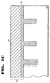
- a substrate 100 is provided.
- Substrate 100 is preferably a monocrystalline silicon wafer.
- Substrate 100 need not necessarily be a silicon wafer and may be other types of substrates such as gallium arsenide or quartz.
- Substrate 100 typically will include a plurality of spaced apart features or holes 102.
- Features 102 can be due to, but not limited to, trenches formed in a substrate, field oxide regions grown on a substrate, and contact and via openings formed in an interlayer dielectric (ILD).
- ILD interlayer dielectric
- the process of the present invention is ideally suited for depositing silicon films in high aspect ratio openings during the formation of trench and/or stacked capacitors in the manufacture of modem high density dynamic random access memories (DRAMS).
- DRAMS modem high density dynamic random access memories
- a substrate 100 is defined as the material onto which a silicon film of the present invention is deposited.
- a substrate such as substrate 100
- the single substrate reactor 300 shown in Figure 3
- Chamber 319 is designed to handle wafers up to 200 mm and has a volume of approximately ten liters, such as used in the Applied Material's Centura single wafer chamber tool. It is to be appreciated that larger volume chambers for handling larger wafers, such as 300 mm, may be used, if desired.
- all flow rates provided herein are with respect to a ten liter chamber and one skilled in the art will recognize the need to scale flow rates for difficult volume reactors. What is important is to utilize the partial pressures of the gases provided herein.
- Substrate 100 is mounted on a pedestal or susceptor 322 that is rotated by a motor (not shown) to provide a time average environment for the substrate 100 that is cylindrically symmetric.
- a susceptor circumscribing preheat ring 324 is supported by sidewall 314 and surrounds susceptor 322 and substrate 100.
- Lifting fingers 323 pass through holes (not shown) form through susceptor 322 to engage the underside of substrate 100 to lift it off susceptor 322.
- Substrate 100 and preheat ring 324 are heated by a light from a plurality of high intensity lamps 326 mounted outside of reactor 310.
- High intensity lamps 326 are preferably tungsten halogen lamps which produce infrared (IR) light at a wavelength of approximately 1.1 ⁇ m (1.1 microns).
- the top 312 and bottom 318 of reactor 310 are substantially transparent to light to enable light from external lamps 326 to enter reactor 310 and heat susceptor 322, substrate 100 and preheat ring 324. Quartz is used for the top 312 and the bottom 318 because it is transparent to light of visible and IR frequency; because it is relatively high strength material that can support a large pressure difference across it; and because it has a low rate of outgassing.
- a suitable top temperature sensor and a suitable bottom temperature sensor, such as pyrometers, are positioned to measure the temperature of substrate 100 and the temperature of susceptor 322, respectively.
- chamber 319 is evacuated through exhaust port 332 by a pump (not shown) to reduce the pressure in chamber 319 from atmospheric pressure to a deposition pressure.
- the deposition pressure is the total pressure within chamber 319 when a silicon film of the present invention is deposited.
- the present invention utilizes a relatively high deposition pressure in order to increase the deposition rate with improved step coverage.
- the deposition pressure of the present invention is between 2666-39997 pascals (20-300 torr), with a pressure of between 19998-26664 pascals (150-200 torr) being preferred. The higher the deposition pressure, the higher will be the deposition rate.
- An increase in deposition pressure increases the step coverage of the process at a fixed growth rate.
- substrate 100, preheat ring 324, and susceptor 322 are heated by lamps 326 to a deposition temperature between 550-620°C with approximately 590-600°C being preferred.
- a deposition temperature between 550-620°C with approximately 590-600°C being preferred.
- the deposition rate decreases and step coverage improves.
- the exact crystallographic nature of the deposited silicon depends upon the deposition temperature.
- the relatively low deposition temperatures utilized in the present invention deposits only amorphous silicon, however at higher deposition temperatures (greater than 610°C), some polysilicon can be incorporated into the film.
- reactant gases are fed into reaction chamber 319.
- the deposition pressure and temperature are maintained within the specified ranges while reactant gases flow into reaction chamber 319 to deposit a silicon film.
- the reactant gas stream flows from a gas input port 328, across a preheat ring 324, where the gases are heated, across the surface of the substrate 100 in the direction of the arrows 330 to deposit silicon films thereon, and out through exhaust port 332.
- the gas input port 328 is connected, via conduit 334, to a gas supply represented by tanks 336 that provides one or a mixture of gases.
- the gas concentrations and/or flow rate through the conduit 334 and each of the ports 338 and 332, are selected to produce processing gas flows and concentration profiles that optimize processing uniformity.
- the rotation of the substrate and the thermal gradients caused by the heat from lamps 326 can significantly affect the flow of the gases in the reactor 300, the dominant shape of the flow profile is a laminar flow from the gas input port 328 and across the preheat ring 324 and the substrate 320 to exhaust port 332.
- the reactant gases comprise a silicon containing gas, a diluted dopant gas, and a carrier gas.
- the silicon containing gas is fed into process chamber 319 to produce a relatively high silicon containing gas partial pressure of greater than 4 torr and less than 5333 pascals (40 torr), with a partial pressure between 1333-2666 pascals (10-20 torr) being preferred.
- a relatively high flow rate of between 500-1500 sccm, with approximately 900 sccm being preferred of silicon containing gas is utilized.
- the high silicon containing gas partial pressure increases the deposition rate of the film. Too high of a partial pressure of silicon containing gas, however, can lead to particles and silicon deposition on chamber sidewalls.
- the silicon containing gas is preferably silane (SiH 4 ), but may be other silicon containing gas, such as but not limited to, disilane (Si 2 H 6 ), dichlorosilane (SiCl 2 H 2 ), trichlorosilane (SiCl 3 H), and tetrachlorosilane (SiCl 4 ).
- a dopant gas is preferably included in the reactant gas mix in order to produce an insitu doped silicon film.
- a dopant gas is fed into reaction chamber 319 to produce a dopant gas partial pressure of between 0-2.7 pascals (0-0.02 torr), with 2 pascals (0.015 torr) being preferred.
- a dopant gas partial pressure of between 0-2.7 pascals (0-0.02 torr), with 2 pascals (0.015 torr) being preferred.
- a relatively low dopant gas partial pressure (less than 2.7 pascals (0.02 torr)) can be used in the present invention because the relatively low process temperature and high deposition pressure employed in the present invention increase the incorporation of dopant in the silicon film.
- addition of a dopant gas decreases the step coverage of the film.
- the present invention preferably utilizes a dopant gas flow rate of between 0.10-2.0 sccm, with 1.0 sccm being preferred.
- the diluted dopant gas is fed into reaction chamber 319 at a rate between 10-200 sccm and preferably at a rate of 100 scan.
- Phosphine (PH 3 ) is the preferred dopant gas, but other dopant gases, such as but not limited to, arsine (AsH 3 ) may be used, if desired.
- the silicon containing gas and the diluted dopant gas are fed into reaction chamber 319 with a carrier gas, such as but not limited to, hydrogen, helium, argon, and nitrogen.
- a carrier gas such as but not limited to, hydrogen, helium, argon, and nitrogen.
- the silicon containing gas and the diluted dopant gas are added to a carrier gas which flows into reaction chamber 319 at a rate of between 4-12 slm (standards liter per minute) and preferably at a rate of 8 slm.
- Reactant gases are fed into reaction chamber 319, until a silicon film 104 of a desired thickness (T) is deposited over substrate 100.
- substrate 100 can be annealed, if desired.
- Substrate 100 can be annealed in order to convert the as deposited amorphous silicon or amorphous/polysilicon film 104 into low resistance polycrystalline silicon.
- an amorphous silicon film can be deposited at a relatively low temperature, in order to improve the step coverage of the film and ensure complete hole filling, and subsequently be converted by annealing into a low resistance polycrystalline silicon film. Any well known method and equipment can be utilized to anneal substrate 100.
- substrate 100 can be annealed in the furnace at about 850°C for 30 minutes in a nitrogen ambient.
- annealing substrate 100 requires an additional step, many integrated circuit manufacturing processes, such as DRAM processes, require subsequent anneals for other purposes, such as silicide formation, and so the anneal step can be included without affecting throughput.
- Utilizing the anneal step of the present invention allows a low resistance polycrystalline film to be formed in a high aspect ratio opening without void formation.
- the process of the present invention can form a high quality polysilicon or amorphous silicon film with a high dopant density (> 2x10 20 /cm 3) and therefore, a low resistivity (between 0.7-1.0 m ⁇ -cm) at a high deposition rate (between 50-120 nm/minute (500-1200 ⁇ /minute)) and with excellent step coverage (between 80-95%).
- the present invention can be reliably used to fill openings in substrate 100 having a width ⁇ 0.28 ⁇ m (0.28 microns) and an aspect ratio ⁇ 2.0 at a high deposition rate without creating voids therein.
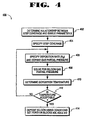
- a method of optimizing deposition conditions of the present invention for specific manufacturing requirements utilizing the single parameter X of the present invention is set forth in flow chart 400 of Figure 4.
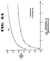
- the first step is to determine the relationship between the single parameter X and step coverage for a specific substrate pattern or topography. This can be accomplished, for example, by depositing a film 510 under a first set of conditions (i.e. silicon gas partial pressure and dopant gas partial pressure) over a substrate, such as substrate 500 shown in Figure 5a.
- Step Coverage vs. X should be generated for each different substrate pattern. This is because step coverage, for a given set of process conditions, will vary depending upon the specific substrate pattern or topography.
- substrate 500 shown in Figure 5a has openings 502 with tapered sidewalls 504. That is, each opening 502 has sidewalls 504 angled at about 94° ( ⁇ ) from the bottom 506 of opening 502. Slightly inclining the sidewall 504 improves step coverage of a film for a given process as compared to an opening having 90° angle.
- Some substrate patterns such as substrate 520 shown in Figure 5b, which have openings 522 which are wider in the middle than at the bottom or the top, are very difficult to obtain good step coverage no matter what process conditions are utilized.
- a silicon film 524 formed on these substrates will exhibit a lower step coverage for a given value of X than on a substrate with an easy to fill pattern, such as substrate 500. Since the step coverage for a given set of process conditions (i.e. value X) will vary depending upon the substrate pattern or topography, it is necessary to generate a different plot for each different substrate pattern.
- a Process Engineer determines what step coverage will be required in order to adequately fill the openings 502 in substrate 500. Once a step coverage is specified, as set forth in block 406, the plot shown in Figure 6a is utilized to determine the value of X which will obtain the specified step coverage.
- a deposition rate for the process is specified.
- the deposition rate (Rd) will typically be dictated by the throughput (number of wafers processed/time) which makes the process most cost effective.
- the dopant gas partial pressure is specified.
- the dopant gas partial pressure will be dictated by the resistivity desired of the silicon film.
- the silicon containing gas partial pressure can be solved for by utilizing Applicant's novel equation (X), as set forth in block 408.
- the deposition temperature of the process is determined.
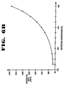
- the deposition temperature can be determined by first generating a plot 610 of Deposition Rate vs. Deposition Temperature, as shown in Figure 6b.
- a plot 610 can be generated by holding constant the conditions set forth in blocks 406 and 408 and then measuring the different growth rates of the films formed at different temperatures. At least three different temperature/growth rate points should be utilized to generate the graph shown in Figure 6b.
- the Deposition Rate vs. Temperature graph of Figure 6b is utilized to determine the temperature necessary to obtain the deposition rate specified in block 408.
- the deposition temperature determined from the graph of Figure 6b is within the specified temperature range of 550-620°C, the temperature is acceptable and, as set forth in block 414, the process conditions are set as determined in blocks 406, 408, and 410. If the temperature required to obtain the desired deposition rate is outside of the acceptable range, however, then the conditions specified in block 406 must be reevaluated. That is, the deposition rate or doping density requirements must be relaxed in order to obtain a feasible process. Thus, not only can the single parameter X of the present invention be utilized to optimize deposition conditions, but it can also be used to determine whether or not a process is even feasible.
- the single parameter X and optimization process of the present invention can be used to set deposition conditions for a silicon deposition process to maximize the manufacturability of the process. For example, if a silicon film is to be deposited on a substrate which has difficult to fill openings, such as substrate 100 with high aspect ratio ( ⁇ 2:1) openings 102 having a width (W) ⁇ 0.5 ⁇ m, a depth of 1.2 ⁇ m and vertical (90°) sidewalls, the relationship between step coverage and the single parameter X indicates that the deposition rates and/or doping density should be reduced in order to maximize the step coverage (> 95%) of the deposited film to ensure complete hole filling.
- ⁇ 2:1 aspect ratio
- a silicon film is to be deposited on a substrate having easy to fill openings or features, such as substrate 500 which has openings 502 having a width of 0.32 ⁇ m (0.32 microns) and a depth of 0.8 ⁇ m (0.8 microns) and with 94° incline sidewalls 504, then the relationship between step coverage and the single parameter X indicates that the deposition rate and/or doping density of the film can be increased since step coverage requirements are reduced. That is, when an easy to fill substrate is encountered, deposition conditions which provide lower values of X can be utilized because step coverage requirements are lessened.
- a silicon film 510 can be deposited onto substrate 500 at a high deposition rate (approximately 110 nm/minute (1100 ⁇ /minute)) and with a high doping density (> 2.0x10 20 /cm 3 ) and completely fill openings 502 by utilizing the deposition conditions of: silane partial pressure of approximately 1733 pascals (13 torr) (silane flow rate of approximately 900 sccm), a phosphine partial pressure of approximately 2 pascals (0.015 torr) (1% hydrogen diluted phosphine flow of approximately 100 scan), a deposition temperature of approximately 620°C, and a deposition pressure of approximately 21332 pascals (160 torr).
- step coverage and the single parameter X can be utilized to design processes where double layer or multilayer silicon films are deposited into high aspect ratio openings ( ⁇ 2.0) in order to improve throughput of the silicon deposition process.
- ⁇ 2.0 aspect ratio openings
- a particular IC manufacturing process requires an 800 nm (8000 ⁇ ) thick(T) silicon film 110, and requires the complete filling of an opening 102 having a width (W) of 0.25 ⁇ m (0.25 microns) and a depth (D) of 750 nm (7500 ⁇ ) (aspect ratio approximately 3.0).
- a first layer of medium doped amorphous silicon (low temperature silicon) layer 112 can be deposited to a thickness of about 150 nm (1500 ⁇ ) in order to maximize the step coverage of the film. That is, in the first deposition step, a high silicon containing gas partial pressure (between 533-5333 pascals (4-40 torr)) is utilized and the deposition rate and doping level of the film are reduced, as specified by the relationship between step coverage and the single parameter X, in order to maximize the step coverage and ensure complete hole filling. (Only approximately 125 nm (1250 ⁇ ) of silicon film is required to fill the opening because the hole fills from the sidewalls, i.e.
- the bulk of the silicon film 114 (remaining 650 nm (6500 ⁇ )) can be deposited with a process, specified by the equation above, to form a polysilicon layer 114 with high doping at a high deposition rate.
- the doping characteristics, step coverage, and deposition rate of each layer 112 and 114 of the composite film 110 are optimized, according to the single parameter X, to suit a particular purpose in order to optimize the entire process.
- the novel parameter (X) can be utilized to maximize wafer throughput and ensure complete hole filling under all manufacturing requirements.
- the single substrate reactor of the present invention preferably includes software stored in a non-volatile memory, such as a ROM, EPROM, etc., which is machine readable and executable by a processor, such as a microprocessor.
- the software is used to control various devices such as pumps, lamps, values, and mass flow controllers in the reactor to produce desired deposition conditions.
- the software preferably includes an algorithm or subroutine which utilizes a relationship between step coverage and the single parameter X, to help an operator optimize and implement a silicon deposition process to meet specific manufacturing requirements.
- the software can be utilized to determine the ideal gas partial pressures (or flow rates) and dopant profiles necessary to meet manufacturing requirements.
- the software and processor can be utilized to control the gas flows and other process parameters, such as temperature and pressure, to carry out an optimal silicon film deposition process.
- the present invention has described a novel process of forming a silicon film at a high deposition rate with improved step coverage in a single substrate reactor.
- the present invention has also described a method and a single parameter which can be utilized to determine optimal process conditions in order to optimize a deposition process for particular manufacturing requirements.
Landscapes
- Chemical & Material Sciences (AREA)
- General Chemical & Material Sciences (AREA)
- Chemical Kinetics & Catalysis (AREA)
- Engineering & Computer Science (AREA)
- Materials Engineering (AREA)
- Mechanical Engineering (AREA)
- Metallurgy (AREA)
- Organic Chemistry (AREA)
- Inorganic Chemistry (AREA)
- Chemical Vapour Deposition (AREA)
- Crystals, And After-Treatments Of Crystals (AREA)
- Electrodes Of Semiconductors (AREA)
Claims (18)
- Verfahren zur Ausbildung einer dotierten Siliziumschicht auf einem Substrat, wobei das Verfahren die Schritte aufweist:Anordnen eines Substrats in einer Reaktionskammer, wobei das Substrat eine Öffnung mit einem Seitenverhältnis von wenigsten 2:1 hat,Erzeugen eines Abscheidedrucks von 2666 bis 39997 Pa (20 bis 300 Torr) in der Reaktionskammer,Erhitzen des Substrats auf eine Temperatur von 550 bis 620 °C,Einströmenlassen eines Silizium enthaltenden Gases in die Reaktionskammer, um einen Partialdruck des Silizium enthaltenden Gases in der Reaktionskammer von 533 bis 5333 Pa (4 bis 40 Torr) zur erhalten, undEinströmenlassen eines Dotiergases in die Reaktionskammer, um einen Partialdruck des Dotiergases von ≤ 2,7 Pa (0,020 Torr) zu erhalten, wodurch die Öffnung mit einem dotierten Siliziumfilm gefüllt wird.
- Verfahren nach Anspruch 1, welches weiterhin den Schritt aufweist:Einströmenlassen von 4 bis 12 slm H2 in die Reaktionskammer.
- Verfahren nach Anspruch 1 oder Anspruch 2, bei welchem die Schritte des Einströmenlassens des Silizium enthaltenden Gases und des Einströmenlassens des Dotiergases ein Gasgemisch erzeugen, das ein Verhältnis von Dotiergas zu Silizium enthaltendem Gas von weniger als oder gleich 0,01 hat.
- Verfahren nach einem der Ansprüche 1 bis 3, bei welchem das Silizium enthaltende Gas Silan ist und der Partialdruck des Silizium enthaltenden Gases 1333 bis 2666 Pa (10 bis 20 Torr) beträgt.
- Verfahren nach einem der Ansprüche 1 bis 4, bei welchem das Dotiergas Phosphin ist und der Partialdruck des Dotiergases etwa 2 Pa (0,015 Torr) beträgt.
- Verfahren nach einem der Ansprüche 1 bis 5, bei welchem der Abscheidedruck 19998 bis 26664 Pa (150 bis 200 Torr) beträgt.
- Verfahren nach einem der Ansprüche 1 bis 6, bei welchem das Substrat auf eine Temperatur von 590 bis 600°C erhitzt wird.
- Verfahren nach einem der Ansprüche 1 bis 7, bei welchem das Silizium enthaltende Gas aus der Gruppe ausgewählt wird, die aus SiH4, Si2H6, SiH2Cl2, SiCl3H und SiCl4 besteht.
- Verfahren zur Ausbildung eines Siliziumfilms, wobei das Verfahren die Schritte aufweist:Anordnen eines Wafers in einer Reaktionskammer, wobei der Wafer eine Öffnung mit einem Seitenverhältnis von wenigstens 2:1 hat,Bestimmen einer Beziehung zwischen einer Stufenüberdeckung eines Siliziumfilms und Abscheidezuständen, zu denen der Partialdruck des Silizium enthaltenden Gases in der Reaktionskammer, der Partialdruck des Dotiergases in der Reaktionskammer und die Abscheiderate des Siliziumfilms gehören, wobei die erwähnte Beziehung die Beziehung zwischen der Stufenüberdeckung und einem Wert χ ist, nämlich(Siliziumgas) pp der Partialdruck des Siliziumgases ist, und 533 bis 5333 Pa (4 bis 40 Torr) beträgt,(Dotiergas) pp der Partialdruck des Dotiergases ist und 0,49 bis 2,7 Pa (0,0037 bis 0,020 Torr) beträgt,∂ = 0,7 bis 0,85,Rd die Abscheiderate ist und 50 bis 120 nm pro Minute (500 bis 1200 Å pro Minute) beträgt, unddie Stufenüberdeckung = TS/TF x 100% ist, wenn TS die Filmdicke an einer Stufenoberfläche und TF die Sollfilmdicke an einer ebenen Oberfläche sind, sowieAbscheiden eines Siliziumfilms auf dem Wafer unter Verwendung der aus der erwähnten Beziehung bestimmten Abscheidezustände,wobei die erwähnte Beziehung zwischen der Stufenüberdeckung und χ für eine spezifische Substratstruktur oder für eine spezifische Topographie bestimmt wird durch(i) Abscheiden eines Siliziumfilms unter einem ersten Satz von Partialdruckzuständen des Siliziumgases und des Dotiergases,(ii) Bestimmen der Abscheiderate und der Stufenüberdeckung durch direkte Messung,(iii) Wiederholen der Schritte (i) und (ii) wenigsten zweimal unter Verwendung eines unterschiedlichen Partialdrucks des Siliziumgases und des Dotiergases und(iv) Auftragen der Stufenüberdeckung als Funktion von χ.
- Vorrichtung zum Abscheiden eines Siliziumfilms auf einem Substrat, das eine Öffnung mit einem Seitenverhältnis von wenigstens 2:1 hat, wobei die Vorrichtungeine Reaktionskammer,einen Suszeptor in der Reaktionskammer,eine Wärmequelle,einen Prozessgaseinlass in die Reaktionskammer undeinen Speicher hat, der eine Beziehung zwischen der Stufenüberdeckung eines Siliziumfilms und Abscheidezuständen speichert, zu denen der Partialdruck des Silizium enthaltenden Gases, der Partialdruck des Dotiergases und die Abscheiderate des Siliziumfilms gehören, wobei die erwähnte Beziehung die Beziehung zwischen der Stufenüberdeckung und einem Wert χ ist, nämlich:(Siliziumgas) pp der Partialdruck des Siliziumgases ist und 533 bis 5333 Pa (4 bis 40 Torr) beträgt,(Dotiergas) pp der Partialdruck des Dotiergases ist und 0,49 bis 2,7 Pa (0,0037 bis 0,020 Torr) beträgt,∂ = 0,7 bis 0,85,Rd die Abscheiderate ist und 50 bis 120 nm pro Minute (500 bis 1200 Å pro Minute) beträgt,die Stufenüberdeckung = TS/TF x 100% ist, wenn TS die Filmdicke an einer Stufenoberfläche und TF die Sollfilmdicke an einer ebenen Oberfläche sind, undwobei die erwähnte Beziehung zwischen der Stufenüberdeckung und χ für eine spezifische Substratstruktur oder für eine spezifische Topographie bestimmt wird durch(i) Abscheiden eines Siliziumfilms unter einem ersten Satz von Partialdruckzuständen des Siliziumgases und des Dotiergases,(ii) Bestimmen der Abscheiderate und der Stufenüberdeckung durch direkte Messung,(iii) Wiederholen der Schritte (i) und (ii) wenigsten zweimal unter Verwendung eines unterschiedlichen Partialdrucks des Siliziumgases und des Dotiergases und(iv) Auftragen der Stufenüberdeckung als Funktion von χ.
- Verfahren zum Abscheiden eines Siliziumfilms auf einem strukturierten Substrat, das eine Öffnung mit einem Seitenverhältnis von wenigstens 2:1 hat, wobei das Verfahren die Schritte aufweist:- wobei die erwähnte Beziehung zwischen der Stufenüberdeckung und χ für eine spezifische Substratstruktur oder für eine spezifische Topographie bestimmt wird durch(a) Bestimmen einer Beziehung zwischen einer Stufenüberdeckung eines Siliziumfilms und Abscheidezuständen, zu denen der Partialdruck des Silizium enthaltenden Gases in der Reaktionskammer, der Partialdruck des Dotiergases in der Reaktionskammer, und die Abscheiderate des auf dem strukturierten Substrat gebildeten Siliziumfilms gehören, wobei die erwähnte Beziehung die Beziehung zwischen der Stufenüberdeckung und einem Wert χ ist, nämlich(Siliziumgas) pp der Partialdruck des Siliziumgases ist und 533 bis 5333 Pa (4 bis 40 Torr) beträgt,(Dotiergas) pp der Partialdruck des Dotiergases ist und 0,49 bis 2,7 Pa (0,0037 bis 0,020 Torr) beträgt,∂ = 0,7 bis 0,85,Rd die Abscheiderate ist und 50 bis 120 nm pro Minute (500 bis 1200 Å pro Minute) beträgt,die Stufenüberdeckung = TS/TF x 100% ist, wenn TS die Filmdicke an einer Stufenoberfläche und TF die Sollfilmdicke an einer ebenen Oberfläche sind,(b) Spezifizieren einer Abscheiderate und eines Partialdrucks für das Dotiergas für die Abscheidung des Siliziumfilms,(c) Spezifizieren einer Stufenüberdeckung des Films,(d) Bestimmen des Partialdrucks des Silizium enthaltenden Gases aus der erwähnten Beziehung, die im Schritt (a) definiert ist, und aus dem Partialdruck des Dotiergases und der Wachstumsrate, die im Schritt (b) definiert sind,(e) Bestimmen der Beziehung zwischen der Abscheiderate des Siliziumfilms und der Abscheidetemperatur unter Verwendung des im Schritt (d) bestimmten Partialdrucks des Siliziumgases und des im Schritt (c) spezifizierten Partialdrucks des Dotiergases für das Abscheiden des Siliziumfilms,(f) Bestimmen der Abscheidetemperatur des Siliziumfilms unter Verwendung der Abscheiderate, die im Schritt (d) spezifiziert ist, und des erwähnten Verhältnisses zwischen der Wachstumsrate und der Abscheidetemperatur, die im Schritt (e) definiert sind, und(g) Abscheiden eines Siliziumfilms auf dem strukturierten Substrat unter Verwendung der aus den Schritten (d) bis (f) bestimmten Abscheidezustände,(i) Abscheiden eines Siliziumfilms unter einem ersten Satz von Partialdruckzuständen des Siliziumgases und des Dotiergases,(ii) Bestimmen der Abscheiderate und der Stufenüberdeckung durch direkte Messung,(iii) Wiederholen der Schritte (i) und (ii) wenigsten zweimal unter Verwendung eines unterschiedlichen Partialdrucks des Siliziumgases und des Dotiergases und(iv) Auftragen der Stufenüberdeckung als Funktion von χ.
- Verfahren nach Anspruch 11, welches weiterhin den Schritt aufweist:Bestimmen, ob die Abscheidetemperatur innerhalb eines spezifizierten Bereichs liegt und wenn nicht, dann Spezifizieren einer zweiten Abscheiderate, wobei die zweite Abscheiderate kleiner als die erste Abscheiderate ist, und Wiederholen der Schritte (c), (d), (e) und (f).
- Verfahren nach Anspruch 11 oder Anspruch 12, welches weiterhin den Schritt aufweist:Bestimmen, ob die Abscheidetemperatur innerhalb eines spezifizierten Bereichs liegt, und wenn nicht, dann Spezifizieren eines zweiten Partialdrucks des Dotiergases, wobei der zweite Partialdruck des Dotiergases kleiner ist als der erste Partialdruck des Dotiergases, und Wiederholen der Schritte (c), (d), (e) und (f).
- Verfahren nach Anspruch 1, bei welchem das Verfahren ein Verfahren zum Ausfüllen einer ein großes Seitenverhältnis aufweisenden Öffnung in einem Substrat mit einem Siliziumfilm in einem Einzelwaferreaktor ist und die Schritte aufweist:Anordnen eines Substrats in einem Einzelsubstratreaktor, wobei das Substrat eine Öffnung mit einem Seitenverhältnis von wenigstens 2:1 hat,Abscheiden eines ersten dotierten Siliziumfilms unter Verwendung eines ersten Abscheidedrucks von 2666 bis 39997 Pa (20 bis 300 Torr), einer ersten Abscheidetemperatur von 550 bis 620°C, eines ersten Partialdrucks von Silizium enthaltenden Gas von 533 bis 5333 Pa (4 bis 40 Torr) und eines ersten Partialdrucks eines Dotiergases für das Abscheiden des ersten Siliziumfilms mit einer ersten Wachstumsrate, undAbscheiden eines zweiten dotierten Siliziumfilms auf dem ersten Siliziumfilm, wobei der zweite Siliziumfilm bei einem zweiten Abscheidedruck, bei einer zweiten Abscheidetemperatur von 550 bis 620°C, bei einem zweiten Partialdruck des Silizium enthaltenden Gases von 533 bis 5333 Pa (4 bis 40 Torr), und bei einem zweiten Partialdruck des Dotiergases abgeschieden wird, um den zweiten Siliziumfilm mit der zweiten Abscheiderate zu erzeugen, wobei die zweite Abscheiderate größer ist als die erste Abscheiderate.
- Verfahren nach Anspruch 14, bei welchem die zweite Abscheidetemperatur größer ist als die erste Abscheidetemperatur.
- Verfahren nach Anspruch 14 oder Anspruch 15, bei welchem der zweite Partialdruck des Dotiergases größer ist als der erste Partialdruck des Dotiergases.
- Verfahren nach einem der Ansprüche 14 bis 16, bei welchem der zweite Abscheidedruck größer ist als der erste Abscheidedruck.
- Verfahren nach einem der Ansprüche 14 bis 17, bei welchem die Stufenüberdeckung des ersten Siliziumfilms besser ist als die Stufenüberdeckung des zweiten Siliziumfilms.
Applications Claiming Priority (2)
| Application Number | Priority Date | Filing Date | Title |
|---|---|---|---|
| US08/631,922 US5863598A (en) | 1996-04-12 | 1996-04-12 | Method of forming doped silicon in high aspect ratio openings |
| US631922 | 1996-04-12 |
Publications (2)
| Publication Number | Publication Date |
|---|---|
| EP0801148A1 EP0801148A1 (de) | 1997-10-15 |
| EP0801148B1 true EP0801148B1 (de) | 2003-06-11 |
Family
ID=24533335
Family Applications (1)
| Application Number | Title | Priority Date | Filing Date |
|---|---|---|---|
| EP97302514A Expired - Lifetime EP0801148B1 (de) | 1996-04-12 | 1997-04-11 | Verfahren und Vorrichtung zum Herstellen von Siliciumschichten |
Country Status (4)
| Country | Link |
|---|---|
| US (1) | US5863598A (de) |
| EP (1) | EP0801148B1 (de) |
| JP (1) | JP4023865B2 (de) |
| DE (1) | DE69722700T2 (de) |
Families Citing this family (23)
| Publication number | Priority date | Publication date | Assignee | Title |
|---|---|---|---|---|
| US5966627A (en) * | 1996-08-30 | 1999-10-12 | Lucent Technologies Inc. | In-situ doped silicon layers |
| US6232196B1 (en) * | 1998-03-06 | 2001-05-15 | Asm America, Inc. | Method of depositing silicon with high step coverage |
| JP2000114250A (ja) * | 1998-08-21 | 2000-04-21 | Texas Instr Inc <Ti> | 枚葉式反応器を使用した、インサイチュ・ド―ピングされたきめの粗い多結晶シリコンの製法 |
| US6410090B1 (en) | 1998-09-29 | 2002-06-25 | Applied Materials, Inc. | Method and apparatus for forming insitu boron doped polycrystalline and amorphous silicon films |
| WO2001071784A1 (en) | 2000-03-17 | 2001-09-27 | Hitachi, Ltd. | Method of manufacturing semiconductor and manufacturing apparatus |
| JP3707726B2 (ja) * | 2000-05-31 | 2005-10-19 | Hoya株式会社 | 炭化珪素の製造方法、複合材料の製造方法 |
| AU2002306436A1 (en) * | 2001-02-12 | 2002-10-15 | Asm America, Inc. | Improved process for deposition of semiconductor films |
| US7026219B2 (en) * | 2001-02-12 | 2006-04-11 | Asm America, Inc. | Integration of high k gate dielectric |
| US6656838B2 (en) | 2001-03-16 | 2003-12-02 | Hitachi, Ltd. | Process for producing semiconductor and apparatus for production |
| US6984574B2 (en) * | 2002-01-23 | 2006-01-10 | Mosel Vitelic, Inc. | Cobalt silicide fabrication using protective titanium |
| US7186630B2 (en) * | 2002-08-14 | 2007-03-06 | Asm America, Inc. | Deposition of amorphous silicon-containing films |
| DE102004007409B4 (de) * | 2004-02-16 | 2006-06-01 | Infineon Technologies Ag | Überkonformes Herstellungsverfahren für eine Halbleiterstruktur |
| JP4655495B2 (ja) * | 2004-03-31 | 2011-03-23 | 東京エレクトロン株式会社 | 成膜方法 |
| US7294320B2 (en) | 2004-09-17 | 2007-11-13 | Applied Materials, Inc. | Hydrogen peroxide abatement of metal hydride fumes |
| US20070169687A1 (en) * | 2006-01-26 | 2007-07-26 | Caracal, Inc. | Silicon carbide formation by alternating pulses |
| US7959707B2 (en) * | 2006-04-28 | 2011-06-14 | Sri International | Methods for producing consolidated materials |
| US9443730B2 (en) | 2014-07-18 | 2016-09-13 | Asm Ip Holding B.V. | Process for forming silicon-filled openings with a reduced occurrence of voids |
| US9837271B2 (en) | 2014-07-18 | 2017-12-05 | Asm Ip Holding B.V. | Process for forming silicon-filled openings with a reduced occurrence of voids |
| US10460932B2 (en) | 2017-03-31 | 2019-10-29 | Asm Ip Holding B.V. | Semiconductor device with amorphous silicon filled gaps and methods for forming |
| US10593543B2 (en) * | 2017-06-05 | 2020-03-17 | Applied Materials, Inc. | Method of depositing doped amorphous silicon films with enhanced defect control, reduced substrate sensitivity to in-film defects and bubble-free film growth |
| US10559650B2 (en) * | 2018-01-23 | 2020-02-11 | Texas Instruments Incorporated | Trench capacitor with warpage reduction |
| US10586844B2 (en) * | 2018-01-23 | 2020-03-10 | Texas Instruments Incorporated | Integrated trench capacitor formed in an epitaxial layer |
| US11145509B2 (en) | 2019-05-24 | 2021-10-12 | Applied Materials, Inc. | Method for forming and patterning a layer and/or substrate |
Citations (6)
| Publication number | Priority date | Publication date | Assignee | Title |
|---|---|---|---|---|
| US3484311A (en) * | 1966-06-21 | 1969-12-16 | Union Carbide Corp | Silicon deposition process |
| US4466992A (en) * | 1982-05-28 | 1984-08-21 | Phillips Petroleum Company | Healing pinhole defects in amorphous silicon films |
| US4742020A (en) * | 1985-02-01 | 1988-05-03 | American Telephone And Telegraph Company, At&T Bell Laboratories | Multilayering process for stress accommodation in deposited polysilicon |
| US5080933A (en) * | 1990-09-04 | 1992-01-14 | Motorola, Inc. | Selective deposition of polycrystalline silicon |
| US5141892A (en) * | 1990-07-16 | 1992-08-25 | Applied Materials, Inc. | Process for depositing highly doped polysilicon layer on stepped surface of semiconductor wafer resulting in enhanced step coverage |
| US5607724A (en) * | 1991-08-09 | 1997-03-04 | Applied Materials, Inc. | Low temperature high pressure silicon deposition method |
Family Cites Families (3)
| Publication number | Priority date | Publication date | Assignee | Title |
|---|---|---|---|---|
| JPS577959A (en) * | 1980-06-19 | 1982-01-16 | Toshiba Corp | Semiconductor device |
| US5614257A (en) * | 1991-08-09 | 1997-03-25 | Applied Materials, Inc | Low temperature, high pressure silicon deposition method |
| JP2658840B2 (ja) * | 1993-12-01 | 1997-09-30 | 日本電気株式会社 | プロセスシミュレータおよびこれを用いたcvd装置およびプロセスシミュレーション方法 |
-
1996
- 1996-04-12 US US08/631,922 patent/US5863598A/en not_active Expired - Lifetime
-
1997
- 1997-04-11 EP EP97302514A patent/EP0801148B1/de not_active Expired - Lifetime
- 1997-04-11 DE DE69722700T patent/DE69722700T2/de not_active Expired - Fee Related
- 1997-04-14 JP JP09612397A patent/JP4023865B2/ja not_active Expired - Fee Related
Patent Citations (6)
| Publication number | Priority date | Publication date | Assignee | Title |
|---|---|---|---|---|
| US3484311A (en) * | 1966-06-21 | 1969-12-16 | Union Carbide Corp | Silicon deposition process |
| US4466992A (en) * | 1982-05-28 | 1984-08-21 | Phillips Petroleum Company | Healing pinhole defects in amorphous silicon films |
| US4742020A (en) * | 1985-02-01 | 1988-05-03 | American Telephone And Telegraph Company, At&T Bell Laboratories | Multilayering process for stress accommodation in deposited polysilicon |
| US5141892A (en) * | 1990-07-16 | 1992-08-25 | Applied Materials, Inc. | Process for depositing highly doped polysilicon layer on stepped surface of semiconductor wafer resulting in enhanced step coverage |
| US5080933A (en) * | 1990-09-04 | 1992-01-14 | Motorola, Inc. | Selective deposition of polycrystalline silicon |
| US5607724A (en) * | 1991-08-09 | 1997-03-04 | Applied Materials, Inc. | Low temperature high pressure silicon deposition method |
Also Published As
| Publication number | Publication date |
|---|---|
| DE69722700D1 (de) | 2003-07-17 |
| US5863598A (en) | 1999-01-26 |
| DE69722700T2 (de) | 2004-05-13 |
| EP0801148A1 (de) | 1997-10-15 |
| JPH1074703A (ja) | 1998-03-17 |
| JP4023865B2 (ja) | 2007-12-19 |
Similar Documents
| Publication | Publication Date | Title |
|---|---|---|
| US5863598A (en) | Method of forming doped silicon in high aspect ratio openings | |
| US7713881B2 (en) | Process sequence for doped silicon fill of deep trenches | |
| KR100652909B1 (ko) | 하이 스텝 커버리지를 갖는 실리콘 증착 방법 | |
| US6488776B2 (en) | Method and apparatus for forming insitu boron doped polycrystalline and amorphous silicon films | |
| US7297641B2 (en) | Method to form ultra high quality silicon-containing compound layers | |
| US7112538B2 (en) | In situ growth of oxide and silicon layers | |
| KR100272891B1 (ko) | 저온, 고압 상태에서의 실리콘 증착방법 | |
| US20070232031A1 (en) | UV assisted low temperature epitaxial growth of silicon-containing films | |
| JP2002110572A (ja) | マルチデポジションsacvdリアクタ | |
| EP0785574A2 (de) | Herstellungsverfahren von Wolfram-Silizid | |
| EP1044291B1 (de) | In situ wachstum von oxid und silizium schichten | |
| US5783257A (en) | Method for forming doped polysilicon films | |
| EP1100978A1 (de) | Verfahren und vorrichtung zur herstellung amorpher und polykristalliner schichten aus silizium-germanium legierungen | |
| KR20050107510A (ko) | 에피텍셜 반도체 증착 방법 및 구조 | |
| US6198167B1 (en) | Semiconductor structure exhibiting reduced contact resistance and method for fabrication | |
| EP4667616A1 (de) | Verfahren zur herstellung von dünnschichten unter verwendung von zwei arten von siliciumvorläufern | |
| Fitch et al. | Morphology and Step Coverage of in-situ doped polysilicon films deposited by single wafer CVD | |
| KR960016220B1 (ko) | 반도체 장치의 제조 방법 | |
| John | Chemical vapour deposition |
Legal Events
| Date | Code | Title | Description |
|---|---|---|---|
| PUAI | Public reference made under article 153(3) epc to a published international application that has entered the european phase |
Free format text: ORIGINAL CODE: 0009012 |
|
| AK | Designated contracting states |
Kind code of ref document: A1 Designated state(s): DE GB |
|
| 17P | Request for examination filed |
Effective date: 19980311 |
|
| 17Q | First examination report despatched |
Effective date: 19990819 |
|
| GRAH | Despatch of communication of intention to grant a patent |
Free format text: ORIGINAL CODE: EPIDOS IGRA |
|
| GRAH | Despatch of communication of intention to grant a patent |
Free format text: ORIGINAL CODE: EPIDOS IGRA |
|
| GRAA | (expected) grant |
Free format text: ORIGINAL CODE: 0009210 |
|
| AK | Designated contracting states |
Designated state(s): DE GB |
|
| REG | Reference to a national code |
Ref country code: GB Ref legal event code: FG4D |
|
| REF | Corresponds to: |
Ref document number: 69722700 Country of ref document: DE Date of ref document: 20030717 Kind code of ref document: P |
|
| PG25 | Lapsed in a contracting state [announced via postgrant information from national office to epo] |
Ref country code: GB Free format text: LAPSE BECAUSE OF NON-PAYMENT OF DUE FEES Effective date: 20040411 |
|
| PLBE | No opposition filed within time limit |
Free format text: ORIGINAL CODE: 0009261 |
|
| STAA | Information on the status of an ep patent application or granted ep patent |
Free format text: STATUS: NO OPPOSITION FILED WITHIN TIME LIMIT |
|
| 26N | No opposition filed |
Effective date: 20040312 |
|
| GBPC | Gb: european patent ceased through non-payment of renewal fee |
Effective date: 20040411 |
|
| PGFP | Annual fee paid to national office [announced via postgrant information from national office to epo] |
Ref country code: DE Payment date: 20080430 Year of fee payment: 12 |
|
| PG25 | Lapsed in a contracting state [announced via postgrant information from national office to epo] |
Ref country code: DE Free format text: LAPSE BECAUSE OF NON-PAYMENT OF DUE FEES Effective date: 20091103 |