EP0800283A2 - Funksender Empfänger für Senden und Empfang von MF Signalen in zwei Bändern - Google Patents
Funksender Empfänger für Senden und Empfang von MF Signalen in zwei Bändern Download PDFInfo
- Publication number
- EP0800283A2 EP0800283A2 EP97660033A EP97660033A EP0800283A2 EP 0800283 A2 EP0800283 A2 EP 0800283A2 EP 97660033 A EP97660033 A EP 97660033A EP 97660033 A EP97660033 A EP 97660033A EP 0800283 A2 EP0800283 A2 EP 0800283A2
- Authority
- EP
- European Patent Office
- Prior art keywords
- signal
- frequency
- mixing
- transmitter
- frequency band
- Prior art date
- Legal status (The legal status is an assumption and is not a legal conclusion. Google has not performed a legal analysis and makes no representation as to the accuracy of the status listed.)
- Granted
Links
Images

Classifications
-
- H—ELECTRICITY
- H04—ELECTRIC COMMUNICATION TECHNIQUE
- H04B—TRANSMISSION
- H04B1/00—Details of transmission systems, not covered by a single one of groups H04B3/00 - H04B13/00; Details of transmission systems not characterised by the medium used for transmission
- H04B1/005—Details of transmission systems, not covered by a single one of groups H04B3/00 - H04B13/00; Details of transmission systems not characterised by the medium used for transmission adapting radio receivers, transmitters andtransceivers for operation on two or more bands, i.e. frequency ranges
- H04B1/0053—Details of transmission systems, not covered by a single one of groups H04B3/00 - H04B13/00; Details of transmission systems not characterised by the medium used for transmission adapting radio receivers, transmitters andtransceivers for operation on two or more bands, i.e. frequency ranges with common antenna for more than one band
- H04B1/006—Details of transmission systems, not covered by a single one of groups H04B3/00 - H04B13/00; Details of transmission systems not characterised by the medium used for transmission adapting radio receivers, transmitters andtransceivers for operation on two or more bands, i.e. frequency ranges with common antenna for more than one band using switches for selecting the desired band
-
- H—ELECTRICITY
- H03—ELECTRONIC CIRCUITRY
- H03D—DEMODULATION OR TRANSFERENCE OF MODULATION FROM ONE CARRIER TO ANOTHER
- H03D7/00—Transference of modulation from one carrier to another, e.g. frequency-changing
- H03D7/16—Multiple-frequency-changing
- H03D7/165—Multiple-frequency-changing at least two frequency changers being located in different paths, e.g. in two paths with carriers in quadrature
-
- H—ELECTRICITY
- H03—ELECTRONIC CIRCUITRY
- H03J—TUNING RESONANT CIRCUITS; SELECTING RESONANT CIRCUITS
- H03J5/00—Discontinuous tuning; Selecting predetermined frequencies; Selecting frequency bands with or without continuous tuning in one or more of the bands, e.g. push-button tuning, turret tuner
- H03J5/02—Discontinuous tuning; Selecting predetermined frequencies; Selecting frequency bands with or without continuous tuning in one or more of the bands, e.g. push-button tuning, turret tuner with variable tuning element having a number of predetermined settings and adjustable to a desired one of these settings
- H03J5/0245—Discontinuous tuning using an electrical variable impedance element, e.g. a voltage variable reactive diode, in which no corresponding analogue value either exists or is preset, i.e. the tuning information is only available in a digital form
- H03J5/0272—Discontinuous tuning using an electrical variable impedance element, e.g. a voltage variable reactive diode, in which no corresponding analogue value either exists or is preset, i.e. the tuning information is only available in a digital form the digital values being used to preset a counter or a frequency divider in a phase locked loop, e.g. frequency synthesizer
-
- H—ELECTRICITY
- H04—ELECTRIC COMMUNICATION TECHNIQUE
- H04B—TRANSMISSION
- H04B1/00—Details of transmission systems, not covered by a single one of groups H04B3/00 - H04B13/00; Details of transmission systems not characterised by the medium used for transmission
- H04B1/005—Details of transmission systems, not covered by a single one of groups H04B3/00 - H04B13/00; Details of transmission systems not characterised by the medium used for transmission adapting radio receivers, transmitters andtransceivers for operation on two or more bands, i.e. frequency ranges
-
- H—ELECTRICITY
- H04—ELECTRIC COMMUNICATION TECHNIQUE
- H04B—TRANSMISSION
- H04B1/00—Details of transmission systems, not covered by a single one of groups H04B3/00 - H04B13/00; Details of transmission systems not characterised by the medium used for transmission
- H04B1/38—Transceivers, i.e. devices in which transmitter and receiver form a structural unit and in which at least one part is used for functions of transmitting and receiving
- H04B1/40—Circuits
- H04B1/403—Circuits using the same oscillator for generating both the transmitter frequency and the receiver local oscillator frequency
- H04B1/406—Circuits using the same oscillator for generating both the transmitter frequency and the receiver local oscillator frequency with more than one transmission mode, e.g. analog and digital modes
Definitions
- the object of the invention is a transmitter/receiver for transmitting and receiving an RF signal in two operating frequency bands.
- Mobile station systems have developed and expanded at an extremely rapid rate, which is the reason why a variety of systems using many different standards have been or are being constructed in many areas. This has generated the need for mobile stations which can use more than one system.
- digital GSM system and DCS that is PCN system which operate in different frequency bands but whose specifications are otherwise similar to each other.
- a radio frequency signal is converted directly to a baseband without there being any intermediate frequency. Since no intermediate frequency stages are needed, only a few components are needed in the receiver, which makes it a preferable solution for various applications. However, in mobile stations, direct conversion receivers have so far rarely been used.
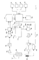
- Fig. 1 shows a prior known schematic block diagram of a transmitter/receiver of a mobile station and in this block diagram the receiver is a so-called direct conversion receiver.
- An RF signal received by an antenna 138 is conducted via a duplex filter 102 to a pre-amplifier 104.
- the purpose of the duplex filter is to permit the use of the same antenna both in transmitting and receiving.
- a synchronous antenna changeover switch can be used in a time-division system.
- the RF signal which is received from the amplifier 104 is low-pass or band pass filtered 106 and demodulated in an I/Q demodulator 108 into an in-phase signal 108a and into a quadrature signal 108b.
- a local oscillator signal 114b which is needed in the demodulation is received from a synthesizer 114.
- Block 110 removal of dc-voltage as well as automatic gain control AGC are carried out.
- Block 110 is controlled by a processing block 116 which may contain, for example, a microprocessor and/or a digital signal processor DSP.
- Automatic gain control is regulated by a signal 110a and removal of the offset voltage is regulated by a signal 110b.
- Signals received from block 110 are converted into digital signals in block 112 from which the signals are further transferred to digital signal processing circuits in the processing block 116.
- the transmitter unit comprises an I/Q modulator 128. This takes an in-phase signal 128a and a quadrature signal 128b and creates a carrier frequency signal which is low-pass filtered and/or high-pass filtered by a filter 130.
- the carrier frequency signal is amplified by an RF amplifier 132 and the amplified signal is transferred via a duplex filter 102 to an antenna 138.
- a power control unit 134 of the transmitter controls the amplification of the RF amplifier 132 on the basis of the measured output power 136 and of the control 134a received from the processor.
- Fig. 1 also shows, attached to the processing unit, a memory unit 126 and user interface means which comprise a display 118, a keyboard 120, a microphone 122 and an earpiece 124.
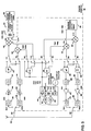
- Fig. 2 shows a novel solution for the implementation of a transmitter/receiver which operates in two frequency bands.
- An RF signal received by the antenna is connected either to the DCS branch or to the GSM branch of the circuit via a switch 204. If a DCS frequency band signal is being received, the received signal is conducted to a band pass filter 206, to a low noise amplifier LNA 208 and to a band pass filter 210. Thereafter, components which are separated by a phase shift of 90 degrees are formed from the signal in block 212.
- the in-phase component I and the quadrature component Q are conducted further by switches 214 and 234 to mixers 216 and 236.
- a mixing signal for the mixers is obtained from a DCS synthesizer 240, the frequency of which corresponds to the received carrier frequency and then an in-phase and a quadrature component of a complex baseband signal are obtained as a result of this mixing process.
- the baseband signal is processed further in a processing unit of a received signal, which means an RX signal, block 239.
- the switch 204 controls the received signal to the GSM branch in which there are, respectively connected in series, a band pass filter 226, a low noise amplifier 228, a band pass filter 230 and a phase shifter 232 which forms two signals which are separated by a phase difference of 90 degrees.
- the signals are conducted further, controlled by the switches 214 and 234, to the mixers 216 and 236 in which a signal selected by a switch 261 and obtained from a GSM synthesizer 250 is now used as mixing frequency.
- Signals obtained from the mixers are conducted further to the processing unit 239 of a baseband received signal, which means an RX signal.
- the DCS synthesizer is formed, as known, from a phase locked loop PLL which comprises a voltage controlled oscillator VCO 241, the output signal of which is amplified by an amplifier 246 for forming an output signal.
- the frequency of a signal transmitted by the oscillator 241 is divided by an integer Y in a divider 242 and the resulting signal is conducted to a phase comparator 243.
- the frequency of the signal formed by a reference oscillator 258 is divided by an integer X in a divider 244 and conducted to the phase comparator 243.
- the phase comparator produces a signal which is proportional to the phase difference of said two input signals and which has been conducted to a low pass filter LPF 245, and the filtered signal controls further the voltage controlled oscillator 241.
- the above described phase locked loop operates in a known manner so that the output frequency of the synthesizer becomes locked to the frequency which is led to the phase comparator from the reference frequency branch.
- the output frequency is controlled by changing the dividing number Y
- the GSM synthesizer 250 comprises respectively a voltage controlled oscillator 250, an amplifier 256, dividers 252 and 254, a phase comparator 253 and a low pass filter 255.
- the GSM synthesizer operates in a similar way as the above described DCS synthesizer but the output frequency of the GSM synthesizer corresponds to GSM frequency bands.
- the baseband complex transmitting signal which means the TX signal
- the processing unit of a TX signal and from there the in-phase and the quadrature component of the signal are conducted to mixers 262 and 282 in which a carrier frequency signal is formed by multiplying the input signal by the mixing signal.
- the output signal of the DCS synthesizer is selected via a switch 261 as a mixing signal.
- the carrier frequency signal is conducted via a switch 264 to the DCS branch in which a phase shift of 90 degrees is formed first between the in-phase component and the quadrature component, and after this, the received signals are summed, block 266.
- the formed DCS signal is conducted to a band pass filter 268, to an amplifier 270 and to a band pass filter 272.
- the formed RF signal is conducted further to an antenna 202 via a switch 280.
- the output signal of the GSM synthesizer is used as the mixing signal.
- the received carrier frequency signal is conducted to the GSM branch in which a similar processing occurs as in the DCS branch in blocks 286, 288, 290 and 292.
- the formed RF signal is conducted to the antenna 202 via the switch 280.
- the transmitting and the receiving circuits have to be connected to the antenna, for example, via a Duplex filter as in the arrangement shown in Fig. 1.
- filters are needed for each frequency band.
- a synchronized antenna changeover switch can be used in a time-division system.
- phase accuracy Another problem connected to the above presented solution is achieving an adequate phase accuracy.
- the accuracy demand for the phase difference between the I and the Q components is only of a few degrees' magnitude. Since in conventional RC phase shifters, factors on which the phase shift depends include the frequency and the temperature of the components, it is difficult to achieve an adequate phase accuracy throughout the entire frequency band and in all operating conditions. In addition, operating in two frequency bands which are far from each other complicates the controlling of the phase accuracy.
- One solution is to form signals in different phases of a higher oscillator frequency by dividing the signals in which case a better phase accuracy is achieved which is independent on the frequency.
- the disadvantage of this solution is, however, that when operating, for example, in the 2 GHz frequency band, one would need a synthesizer with an output frequency of 4 GHz which is such a high frequency value that the implementation of the synthesizer and the frequency dividers would become extremely complicated.
- the aim of the invention is to devise a simple solution for the implementation of a transmitter/receiver which operates in two frequency bands so that the above presented disadvantages connected to the solutions according to the prior art can be avoided.
- One idea of the invention is to use a transmitter/receiver which is based on direct conversion and in which the mixing frequency is formed by means of the same synthesizer when operating in two frequency bands.
- This is implemented preferably in such a way that in the higher, first operating frequency band, the frequency of the output signal of the synthesizer is used as such as a mixing frequency and when operating in the lower, second operating frequency band, a mixing frequency is used which is obtained by dividing the frequency of the output signal of the synthesizer by at least two.
- two mixing signals which are separated by a phase difference of 90 degrees can be formed in the context of the dividing of the synthesizer frequency in which case no RC phase shifters in the signal line are needed and an excellent phase accuracy is achieved.
- a direct conversion transmitter/receiver which operates in two separate frequency bands and in which the first frequency band comprises the first transmitting frequency band and the first receiving frequency band and the second frequency band comprises the second transmitting frequency band and the second receiving frequency band, and in which
- Figs. 1 and 2 were already described above.
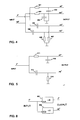
- a transmitter/receiver according to the invention is described by means of Fig. 3.
- some possible ways of implementation for forming signals of different phases in a transmitter/receiver according to the invention are described by referring to Figs. 4-6.
- Fig. 3 shows a block diagram of a transmitter/receiver according to the invention.
- an RF signal received by an antenna is connected either to the DCS branch of the circuit or to the GSM branch via a switch 304. If a DCS frequency band signal is received, the received signal is conducted to a band pass filter 306 of the DCS branch, to a low noise amplifier LNA 308 and to a band pass filter 310. After this, components which are separated by a phase shift of 90 degrees are formed from the signal in block 312. The in-phase component I and the quadrature component Q are conducted further via switches 314 and 334 to mixers 316 and 336.
- the circuit arrangement corresponds to the circuit arrangement shown in Fig. 2.
- a mixing signal for the mixers is obtained from a synthesizer 340, the frequency of which corresponds to the received carrier frequency and then, as a mixing result, an in-phase and a quadrature component of a complex baseband signal are obtained.
- the baseband signal is conducted further to an automatic gain control block AGC 337 and to an offset voltage correcting block 338. After this, the signal is processed further in a baseband processing unit of a received signal, which means an RX signal, block 339.
- the switch 304 controls the received signal to the GSM branch in which there are respectively connected in series a band pass filter 326, a low noise amplifier 328 and a band pass filter 330. Thereafter, the signal is conducted cophasal to mixers 316 and 336.
- the signal which is received from the synthesizer is now selected via switches 315 and 335 as a mixing frequency, and the frequency of the signal has been divided by two in block 311.
- blocks 311 signals which are separated by a phase shift of 90 degrees are formed out of the signal to mixers 316 and 336. Thus the phase shift of 90 degrees which is needed in the mixing is not carried out to the received signal but rather to the mixing signal.
- a baseband complex signal which is received from the mixers is conducted further to a processing unit 339 of a baseband, received signal that is an RX signal.
- the synthesizer 340 operates in a similar way as the DCS synthesizer shown in Fig. 2. It comprises thus a voltage controlled oscillator VCO 341, the output signal of which is amplified by an amplifier 346 to form an output signal.
- VCO 341 the output signal of which is amplified by an amplifier 346 to form an output signal.
- the frequency of the signal produced by an oscillator 31 is divided by an integer Y in a divider 342 and the resulting signal has been conducted to a phase comparator 343.
- the frequency of a signal formed by a reference oscillator 358 is divided by an integer X in a divider 344 and is conducted to the phase comparator 343.
- the phase comparator produces a signal which is proportional to the phase difference of said two input signals and which has been conducted to a low pass filter 345, and the filtered signal controls further the voltage controlled oscillator 341.
- the output frequency is controlled by changing the dividing number Y.
- the baseband complex transmitting signal which means the TX signal
- the processing unit 360 of a TX signal and from there, the complex components of the signal are conducted to mixers 362 and 382 in which a carrier frequency signal is formed by multiplying the input signal by a mixing signal.
- the output signal of the synthesizer 340 is selected as a mixing signal via switches 363 and 383.
- the formed DCS signal is conducted to a band pass filter 368, to an amplifier 370 and to a band pass filter 372.
- the formed RF signal is conducted further to an antenna 302 via a switch 380.
- the mixing signal is formed by dividing the frequency of the output signal of the synthesizer 340 by two in the divider 361 from which mixing signals are obtained which are separated by a phase shift of 90 degrees to the first TX mixer 362 and to the second TX mixer 382.
- the carrier frequency signal is conducted via switches 364 and 384 to the GSM branch in which the in-phase component and the quadrature component which have been received from the mixers 362 and 382 are summed together, block 386. After this, filtering and amplification proceed in blocks 388, 390 and 392.
- the formed RF signal is conducted to the antenna 302 via the switch 380. In the GSM frequency, the phase shift of 90 degrees is thus processed to the mixing signal and not to the carrier frequency signal which has been obtained as a mixing result.
- the mixing signals of the receiving and the transmitting can be formed by means of the same frequency divider.
- the outputs of different phases of the frequency divider can be connected either to the RX mixers of the receiver during the receiving or to the TX mixers of the transmitter during the transmitting, for example, by using controllable switches.
- the switches are controlled by a signal which is in the first state during the time slot of the receiving and in the second state during the time slot when it is transmitting.
- Another option, when one divider is used is to control the signals received from the divider to the mixers of both the transmitter and the receivers during both the transmitting and the receiving. In this case, the signals can be routed to said mixers by using a dividing means such as a power divider.
- Change-over switches 314, 334, 315, 335, 363, 383, 364 and 384 are controlled most preferably by a two-level signal BC (Band Control).
- BC Battery Control
- the change-over switches are in a position in which high frequency circuits of the first frequency band are used and in the second level of the control signal the change-over switches are in a position in which high frequency circuits of the second frequency band are used.
- the values corresponding to the first and the second level of the control signal BC depend, among others, on the implementation of the change-over switches.
- change-over switches 314, 334, 315, 335, 363, 383, 364 and 384 also some other known method can be applied for controlling the path of the high frequency signal.
- the change-over switches can be substituted, for example, by adapter elements which are known per se, in which case when the first frequency band is used, the high frequency circuits of the second frequency band are of high impedance to the signals of the first frequency band. Similarly, when the second frequency band is used, the high frequency circuits of the first frequency band are of high impedance to the signals of the second frequency band. In this case, the high frequency circuits of different frequency bands do not cause mutual interference.
- the signal BC which controls the change-over switches is formed most preferably in the processing block 116 of a mobile station, Fig. 1, which comprises preferably a processor, such as a microprocessor.
- the processing block 116 forms a signal on the basis of a change-over command of the system which the user has fed by using the keyboard 120, Fig. 1.
- the selection of the system can be, for example, menu-based in which case the desired system is chosen by a particular keystroke from the menu shown on the display 118.
- the processing block 116 forms a control signal BC which corresponds to the selected system.
- the change-over command of the system can also be transmitted via the mobile station system in which case the mobile station receives data which has been transmitted by another system.
- the received data may include a system change-over command, and on the basis of it, the processing block changes the system.
- a control program has been stored which monitors the received data and as it detects a system change-over command in the data, it transmits a command to the processing block to convert the control signal BC into the state according to the selecting command.
- the processing block forms additionally a control signal of a synthesizer and with this signal, a dividing number is given to the divider 342 (Fig. 3) of the frequency synthesizer, and this dividing number corresponds to the given channel frequency. Then the divider 342 of the synthesizer forms from the frequency of a voltage controlled oscillator VCO, 341, a phase comparison frequency to a phase comparator 343.
- the channel spacing is 200 kHz in which case 200 kHz is used as a phase comparison frequency.
- the first frequency band comprises the frequency band of the DCS system and the second frequency band comprises the frequency band of the GSM system.
- the band pass range of the band pass filters 306 and 310 of the receiving branch of the first frequency band is approximately 1805-1880 MHz.
- the band pass range of the band pass filters 326 and 328 of the receiving branch of the second frequency band is approximately 925-960 MHz.
- the band pass range of the band pass filters 368 and 372 of the first frequency band is approximately 1710-1785 MHz and the band pass range of the band pass filters of the second frequency band is approximately 880-915 MHz.
- One further possible method for selecting the signal branch is to switch off the supply voltages from that branch which is not in use. This method can be applied both to the transmitter and to the receiver. The advantage of this alternative is that actual selecting switches are not necessarily needed.
- Fig. 4 shows a circuit diagram of a solution for forming signals of different phases in the DCS receiving branch.
- differential signals are used, that is neither of the signal terminals is connected to the ground level.
- This circuit can be used as block 312 in the circuit arrangement of Fig. 3.
- the differential input signal comprises signal lines of 0° and -180° and for each of them a phase shift of -45° and a phase shift of +45° will be processed for forming two signals which are separated by a 90° phase shift.
- Phase shifters of -45° comprise resistors 401 and 402 and capacitors 403 and 404.
- phase shifters of +45° comprise capacitors 405 and 406 as well as resistors 407 and 408.
- Fig. 5 shows a circuit diagram of a solution for forming signals which are separated by a 90° phase shift in an RC phase shift circuit in which one of the signal conductors is connected to the ground level.
- the -45° phase shift is performed by a phase shifter which is formed of a resistor 511 and a capacitor 512
- the +45° phase shift is formed by a phase shifter which is formed of a capacitor 513 and a resistor 514.
- circuits according to Figs. 4 and 5 can be used, on the basis of symmetry, also as block 366 to perform the phase shift of 90 degrees between the input signals and to sum up the received signals. Then the signals move in opposite direction in the circuits, that is the input signals are fed to the right-hand terminals of the circuits shown in the figures and the output signal is obtained from the left-hand terminals.
- Fig. 6 shows a phase shifter which divides the input frequency by two and which can be used in the implementation of blocks 311 and 361.
- the circuit comprises two dividers 601 and 602 in which case the input signal is fed into the noninverting input of the first divider 601 and into the inverting input of the second divider 602. This is how output signals which are separated by a phase difference of 90 degrees are formed, as known.
- Mixers 362 and 382 have been shown individually in the block diagram shown in Fig. 3 but in practice they can be produced by integration to the same circuit in which case two GSM transmitting signals can be summed up, for example, in a common collector resistance of a prior known Gilbert Cell type mixer, and this collector resistance thus functions as a summer 386.
- Another alternative is to have the summing up processed in a switching circuit which connects the signal after the mixers to the GSM or to the DCS branch.
- One preferable method is the implementation of the switches by using parallel transistor stages in which case the selection of signals proceeds, for example, by switching the supply voltage to that transistor stage through which one wishes the signal to pass and by switching the supply voltage off from that stage which one wishes to remain open. These same transistor stages can be used for summing up the signals.
- a third method is to achieve the summing up by using the method shown by Fig. 3 in a separate summer which has been connected to the transmitter chain after the mixer and the GSM/DCS selecting switches.
Priority Applications (1)
| Application Number | Priority Date | Filing Date | Title |
|---|---|---|---|
| EP06122028A EP1737137B1 (de) | 1996-04-01 | 1997-03-20 | Funksender/Empfänger für Senden und Empfang von MF Signalen in zwei Bändern |
Applications Claiming Priority (2)
| Application Number | Priority Date | Filing Date | Title |
|---|---|---|---|
| FI961465A FI100286B (fi) | 1996-04-01 | 1996-04-01 | Lähetin/vastaanotin RF-signaalin lähettämiseksi ja vastaanottamiseksi kahdella taajuusalueella |
| FI961465 | 1996-04-01 |
Related Child Applications (1)
| Application Number | Title | Priority Date | Filing Date |
|---|---|---|---|
| EP06122028A Division EP1737137B1 (de) | 1996-04-01 | 1997-03-20 | Funksender/Empfänger für Senden und Empfang von MF Signalen in zwei Bändern |
Publications (3)
| Publication Number | Publication Date |
|---|---|
| EP0800283A2 true EP0800283A2 (de) | 1997-10-08 |
| EP0800283A3 EP0800283A3 (de) | 2000-05-31 |
| EP0800283B1 EP0800283B1 (de) | 2006-11-29 |
Family
ID=8545760
Family Applications (2)
| Application Number | Title | Priority Date | Filing Date |
|---|---|---|---|
| EP97660033A Expired - Lifetime EP0800283B1 (de) | 1996-04-01 | 1997-03-20 | Funksender Empfänger für Senden und Empfang von MF Signalen in zwei Bändern |
| EP06122028A Expired - Lifetime EP1737137B1 (de) | 1996-04-01 | 1997-03-20 | Funksender/Empfänger für Senden und Empfang von MF Signalen in zwei Bändern |
Family Applications After (1)
| Application Number | Title | Priority Date | Filing Date |
|---|---|---|---|
| EP06122028A Expired - Lifetime EP1737137B1 (de) | 1996-04-01 | 1997-03-20 | Funksender/Empfänger für Senden und Empfang von MF Signalen in zwei Bändern |
Country Status (5)
| Country | Link |
|---|---|
| US (1) | US5896562A (de) |
| EP (2) | EP0800283B1 (de) |
| JP (1) | JPH1032520A (de) |
| DE (2) | DE69737000T2 (de) |
| FI (1) | FI100286B (de) |
Cited By (19)
| Publication number | Priority date | Publication date | Assignee | Title |
|---|---|---|---|---|
| WO1998043366A1 (en) * | 1997-03-24 | 1998-10-01 | Ericsson Inc. | Dual band mobile station |
| WO1999026352A1 (en) * | 1997-11-19 | 1999-05-27 | Ericsson Inc. | Tuning bandwidth minimization for low voltage dual band receiver |
| WO1999026353A1 (en) * | 1997-11-19 | 1999-05-27 | Ericsson, Inc. | Transceiver architecture in a dual band mobile phone |
| EP1001548A1 (de) * | 1998-11-13 | 2000-05-17 | Sagem S.A. | Verfahren zum Einstellen eines mehrfachband Sender-Empfängers für Mobilfunksystem sowie Mobiltelefon |
| US6125268A (en) * | 1997-11-19 | 2000-09-26 | Ericsson Inc. | Tuning bandwidth minimization for low voltage dual band receiver |
| EP1059734A2 (de) * | 1999-06-10 | 2000-12-13 | Nokia Mobile Phones Ltd. | Funksendeempfänger für das Senden und Empfang in mindestens zwei Frequenzbereichen |
| EP1071249A1 (de) * | 1999-07-22 | 2001-01-24 | Alcatel | Verfahren und Vorrichtung zur Modulation in einem Sender |
| EP1102413A2 (de) * | 1999-11-15 | 2001-05-23 | Hitachi, Ltd. | Mehrbandmobilfunkgerät |
| WO2001043275A2 (de) * | 1999-12-07 | 2001-06-14 | Infineon Technologies Ag | Schaltungsanordnung zur direktmodulation |
| US6405024B1 (en) * | 1997-10-29 | 2002-06-11 | Siemens Aktiengesellschaft | Frequency synthesizer with a phase-locked loop for receiving and processing signals in different frequency bands |
| EP1217756A2 (de) * | 2000-10-20 | 2002-06-26 | Sony Corporation | Tragbares Multiband-Endgerät |
| WO2002075941A2 (de) * | 2001-03-15 | 2002-09-26 | Siemens Aktiengesellschaft | Verfahren und vorrichtung zur erzeugung von mobilfunksignalen |
| EP1381163A1 (de) * | 2002-07-12 | 2004-01-14 | Samsung Electronics Co., Ltd. | HF-Mehrbandempfänger unter Verwendung von HF-Breitbandfiltern |
| WO2004021593A1 (en) * | 2002-08-29 | 2004-03-11 | Koninklijke Philips Electronics N.V. | Transceiver apparatus for use in a multi-frequency communication system, base station of a multi-frequency communication system, method for use of the transceiver apparatus, method of transceiving a multi-frequency signal in a multi-frequency communication system |
| WO2005029720A1 (en) * | 2003-09-19 | 2005-03-31 | Koninklijke Philips Electronics N.V. | Multi-band transceiver |
| EP1708372A2 (de) * | 2005-03-29 | 2006-10-04 | Broadcom Corporation | Integrierte Schaltung für ein Direktkonversionsmultibandfunkgerät |
| US7415247B1 (en) | 1998-11-26 | 2008-08-19 | Nokia Corporation | Method and arrangement for transmitting and receiving RF signals through various radio interfaces of communication systems |
| CN100423459C (zh) * | 2002-10-17 | 2008-10-01 | 托马兹技术有限公司 | 多模式接收机 |
| US9883425B2 (en) | 2006-03-27 | 2018-01-30 | Panasonic Intellectual Property Corporation Of America | Sleep-state for mobile terminal and service initiation for mobile terminals in sleep-state |
Families Citing this family (118)
| Publication number | Priority date | Publication date | Assignee | Title |
|---|---|---|---|---|
| EP0865686B1 (de) * | 1996-09-06 | 2004-12-08 | Koninklijke Philips Electronics N.V. | Direktkonversionsempfänger |
| KR100224102B1 (ko) * | 1996-11-28 | 1999-10-15 | 윤종용 | 이중 대역 셀룰러 전화에 이용되는 중간주파수 선택장치 및 방법 |
| JPH10313260A (ja) * | 1997-05-13 | 1998-11-24 | Matsushita Electric Ind Co Ltd | 受信装置 |
| US5974305A (en) | 1997-05-15 | 1999-10-26 | Nokia Mobile Phones Limited | Dual band architectures for mobile stations |
| FI107658B (fi) * | 1997-06-02 | 2001-09-14 | Nokia Mobile Phones Ltd | Biasjänniteohjattuja rinnakkaisia aktiivikomponentteja |
| JP3848445B2 (ja) * | 1997-09-26 | 2006-11-22 | 松下電器産業株式会社 | 複数通信方式対応の無線機 |
| US6163710A (en) * | 1997-10-20 | 2000-12-19 | Ericsson, Inc. | Method and apparatus for compliance to multiple frequency plans |
| US6016422A (en) * | 1997-10-31 | 2000-01-18 | Motorola, Inc. | Method of and apparatus for generating radio frequency quadrature LO signals for direct conversion transceivers |
| JP2001508272A (ja) * | 1997-11-06 | 2001-06-19 | コーニンクレッカ フィリップス エレクトロニクス エヌ ヴィ | 送受信器及び送受信器を有する電気通信システム |
| US6216012B1 (en) * | 1997-11-07 | 2001-04-10 | Conexant Systems, Inc. | Dualband power amplifier control using a single power amplifier controller |
| FI974269A (fi) * | 1997-11-18 | 1999-05-19 | Nokia Mobile Phones Ltd | Kahden taajuusalueen radiolähetin-vastaanotinrakenne |
| CN1246989A (zh) * | 1997-12-05 | 2000-03-08 | 皇家菲利浦电子有限公司 | 一种通信系统,通信装置和频率综合器 |
| US6094579A (en) * | 1998-01-20 | 2000-07-25 | Telefonaktiebolaget Lm Ericsson (Publ) | System and method of mobile station presence verification in a multiple-hyperband cellular telecommunications network |
| US6510310B1 (en) * | 1998-01-26 | 2003-01-21 | Conexant Systems, Inc. | Dual mode phone architecture utilizing a single transmit-receive switch |
| US6275686B1 (en) * | 1998-02-09 | 2001-08-14 | Imogene Healy | Differential phase shift amplifier of electrical or physical quantities |
| JPH11331029A (ja) * | 1998-05-19 | 1999-11-30 | Matsushita Electric Ind Co Ltd | 双方向型無線通信装置およびそれを用いたpcmciaカード型双方向無線通信装置 |
| US6154664A (en) * | 1998-06-24 | 2000-11-28 | Conexant System, Inc. | Dual band cellular phone with two power amplifiers and power control circuit therefore |
| FI981518A (fi) | 1998-07-01 | 2000-01-02 | Nokia Mobile Phones Ltd | Tiedonsiirtomenetelmä ja radiojärjestelmä |
| DE19835893A1 (de) * | 1998-08-07 | 2000-02-17 | Ericsson Telefon Ab L M | Steuerbares Filter |
| US6061551A (en) | 1998-10-21 | 2000-05-09 | Parkervision, Inc. | Method and system for down-converting electromagnetic signals |
| US6091940A (en) | 1998-10-21 | 2000-07-18 | Parkervision, Inc. | Method and system for frequency up-conversion |
| US7515896B1 (en) | 1998-10-21 | 2009-04-07 | Parkervision, Inc. | Method and system for down-converting an electromagnetic signal, and transforms for same, and aperture relationships |
| US6694128B1 (en) | 1998-08-18 | 2004-02-17 | Parkervision, Inc. | Frequency synthesizer using universal frequency translation technology |
| JP2984669B1 (ja) * | 1998-09-11 | 1999-11-29 | 静岡日本電気株式会社 | 簡易携帯電話内蔵型携帯電話機におけるローカル回路 |
| FR2783654B1 (fr) * | 1998-09-23 | 2006-07-28 | Sagem | Emetteur-recepteur bibande a double dispositif de rayonnement |
| US6049706A (en) | 1998-10-21 | 2000-04-11 | Parkervision, Inc. | Integrated frequency translation and selectivity |
| US6542722B1 (en) | 1998-10-21 | 2003-04-01 | Parkervision, Inc. | Method and system for frequency up-conversion with variety of transmitter configurations |
| US6813485B2 (en) | 1998-10-21 | 2004-11-02 | Parkervision, Inc. | Method and system for down-converting and up-converting an electromagnetic signal, and transforms for same |
| US6370371B1 (en) | 1998-10-21 | 2002-04-09 | Parkervision, Inc. | Applications of universal frequency translation |
| US7039372B1 (en) | 1998-10-21 | 2006-05-02 | Parkervision, Inc. | Method and system for frequency up-conversion with modulation embodiments |
| US6061555A (en) | 1998-10-21 | 2000-05-09 | Parkervision, Inc. | Method and system for ensuring reception of a communications signal |
| US6560301B1 (en) | 1998-10-21 | 2003-05-06 | Parkervision, Inc. | Integrated frequency translation and selectivity with a variety of filter embodiments |
| US7236754B2 (en) | 1999-08-23 | 2007-06-26 | Parkervision, Inc. | Method and system for frequency up-conversion |
| US6704549B1 (en) | 1999-03-03 | 2004-03-09 | Parkvision, Inc. | Multi-mode, multi-band communication system |
| US6704558B1 (en) | 1999-01-22 | 2004-03-09 | Parkervision, Inc. | Image-reject down-converter and embodiments thereof, such as the family radio service |
| US6415158B1 (en) * | 1999-02-01 | 2002-07-02 | Lucent Technologies Inc. | Dual mode mobile phone operating as a two-way radio |
| US6298224B1 (en) * | 1999-02-22 | 2001-10-02 | Motorola, Inc. | Multiple frequency band receiver |
| US6879817B1 (en) | 1999-04-16 | 2005-04-12 | Parkervision, Inc. | DC offset, re-radiation, and I/Q solutions using universal frequency translation technology |
| US6853690B1 (en) | 1999-04-16 | 2005-02-08 | Parkervision, Inc. | Method, system and apparatus for balanced frequency up-conversion of a baseband signal and 4-phase receiver and transceiver embodiments |
| US7110444B1 (en) | 1999-08-04 | 2006-09-19 | Parkervision, Inc. | Wireless local area network (WLAN) using universal frequency translation technology including multi-phase embodiments and circuit implementations |
| US7065162B1 (en) | 1999-04-16 | 2006-06-20 | Parkervision, Inc. | Method and system for down-converting an electromagnetic signal, and transforms for same |
| US7693230B2 (en) | 1999-04-16 | 2010-04-06 | Parkervision, Inc. | Apparatus and method of differential IQ frequency up-conversion |
| US6584090B1 (en) * | 1999-04-23 | 2003-06-24 | Skyworks Solutions, Inc. | System and process for shared functional block CDMA and GSM communication transceivers |
| US6560297B1 (en) * | 1999-06-03 | 2003-05-06 | Analog Devices, Inc. | Image rejection downconverter for a translation loop modulator |
| US6728528B1 (en) * | 1999-06-28 | 2004-04-27 | Skyworks Solutions Inc. | Wireless communications device allowing a soft handoff procedure in a mobile communications system |
| US7123891B2 (en) * | 1999-06-28 | 2006-10-17 | Skyworks Solutions, Inc. | Wireless communications device allowing a soft handoff procedure in a mobile communications system |
| US8295406B1 (en) | 1999-08-04 | 2012-10-23 | Parkervision, Inc. | Universal platform module for a plurality of communication protocols |
| CA2289823C (en) * | 1999-11-15 | 2004-07-06 | Philsar Semiconductor Inc. | Complex filtering/agc radio receiver architecture for low-if or zero-if |
| JP4547084B2 (ja) * | 1999-11-15 | 2010-09-22 | ルネサスエレクトロニクス株式会社 | 移動体通信機および送受信機 |
| US6717981B1 (en) * | 1999-12-14 | 2004-04-06 | Koninklijke Philips Electronics N.V. | Transmitter image suppression in TDD transceivers |
| JP4724794B2 (ja) * | 2000-01-19 | 2011-07-13 | エスティー‐エリクソン、ソシエテ、アノニム | ラジオfm受信機 |
| US6473598B1 (en) * | 2000-02-15 | 2002-10-29 | Fareed Sepehry-Fard | Most cost-effective asmmic-based universal microwave and millimeter wave transceiver |
| US7010286B2 (en) | 2000-04-14 | 2006-03-07 | Parkervision, Inc. | Apparatus, system, and method for down-converting and up-converting electromagnetic signals |
| EP1148654A1 (de) | 2000-04-18 | 2001-10-24 | Infineon Technologies AG | Sende- und Empfangseinheit |
| GB2363546B (en) * | 2000-06-14 | 2002-07-03 | Motorola Israel Ltd | Circuit and method for reducing local oscillator frequency transmission in a radio transceiver |
| EP1303055A4 (de) * | 2000-06-26 | 2009-11-04 | Panasonic Corp | Dreifrequenz-verzweigungsschaltung, verzweigungsschaltung und funkkommunikationseinrichtung |
| US6721544B1 (en) * | 2000-11-09 | 2004-04-13 | Intel Corporation | Duplexer structure for coupling a transmitter and a receiver to a common antenna |
| US7454453B2 (en) | 2000-11-14 | 2008-11-18 | Parkervision, Inc. | Methods, systems, and computer program products for parallel correlation and applications thereof |
| US6782249B1 (en) * | 2000-11-22 | 2004-08-24 | Intel Corporation | Quadrature signal generation in an integrated direct conversion radio receiver |
| US6588217B2 (en) * | 2000-12-11 | 2003-07-08 | International Business Machines Corporation | Thermoelectric spot coolers for RF and microwave communication integrated circuits |
| FI20002881A (fi) * | 2000-12-29 | 2002-06-30 | Nokia Corp | Järjestely ja menetelmä radiolähettimen häviöiden vähentämiseksi |
| US6735426B1 (en) | 2001-01-25 | 2004-05-11 | National Semiconductor Corporation | Multiple-band wireless transceiver with quadrature conversion transmitter and receiver circuits |
| US6754508B1 (en) | 2001-01-25 | 2004-06-22 | National Semiconductor Corporation | Multiple-band wireless transceiver with quadrature conversion transmitter and receiver circuits |
| US20020127982A1 (en) * | 2001-03-07 | 2002-09-12 | Nokia Mobile Phones Ltd | Mobile station receiver operable for both single and multi-carrier reception |
| US7024165B2 (en) * | 2001-06-14 | 2006-04-04 | Honeywell Federal Manufacturing & Technologies, Llc | ISM band to U-NII band frequency transverter and method of frequency transversion |
| DE10131676A1 (de) * | 2001-06-29 | 2003-01-16 | Infineon Technologies Ag | Empfängeranordnung mit Wechselstrom-Kopplung |
| JP3672189B2 (ja) * | 2001-07-13 | 2005-07-13 | ソニー株式会社 | 無線信号受信装置及び復調処理回路 |
| EP1434358A4 (de) * | 2001-10-03 | 2004-10-27 | Fujitsu Ltd | Drahtlose vorrichtung mit der fähigkeit zur kommunikation in zwei frequenzbändern und lokaloszillationssignalerzeugungsverfahren in der drahtlosen vorrichtung |
| US7024220B2 (en) * | 2001-10-09 | 2006-04-04 | Kyocera Wireless Corp. | GPS receiver system and method |
| US7072427B2 (en) | 2001-11-09 | 2006-07-04 | Parkervision, Inc. | Method and apparatus for reducing DC offsets in a communication system |
| KR100438556B1 (ko) * | 2001-12-10 | 2004-07-02 | 엘지전자 주식회사 | 트라이 모드 이동 단말기에서의 고주파 신호 처리 장치 및방법 |
| US6980774B2 (en) * | 2002-01-22 | 2005-12-27 | Broadcom, Corp. | Radio frequency integrated circuit |
| GB0204108D0 (en) * | 2002-02-21 | 2002-04-10 | Analog Devices Inc | 3G radio |
| EP1476950B1 (de) * | 2002-02-21 | 2008-08-13 | MediaTek Inc. | Multimode Direktkonversionsempfänger mit einem rekonfigurierbaren Basisband kombinierten Chebychev/inverse Chebychev Filter |
| JP2003298441A (ja) * | 2002-04-01 | 2003-10-17 | Hitachi Ltd | 低消費電力受信装置 |
| DE10228757A1 (de) * | 2002-06-27 | 2004-01-22 | Infineon Technologies Ag | Empfängeranordnung, insbesondere für den Mobilfunk |
| DE10229153A1 (de) * | 2002-06-28 | 2004-02-05 | Epcos Ag | Schaltungsanordnung für ein Mobiltelefon |
| US7460584B2 (en) | 2002-07-18 | 2008-12-02 | Parkervision, Inc. | Networking methods and systems |
| US7379883B2 (en) | 2002-07-18 | 2008-05-27 | Parkervision, Inc. | Networking methods and systems |
| FR2845840B1 (fr) * | 2002-10-14 | 2005-09-16 | St Microelectronics Sa | Dispositif radiofrequence du type a frequence intermediaire nulle ou quasi-nulle minimisant la modulation frequentielle parasite appliquee a un oscillateur local integre. |
| WO2004057768A1 (ja) * | 2002-12-20 | 2004-07-08 | Renesas Technology Corp. | 送信回路およびそれを用いた送受信機 |
| JP4045978B2 (ja) * | 2003-02-25 | 2008-02-13 | 松下電器産業株式会社 | デジタル信号送受信機 |
| KR20050106454A (ko) * | 2003-02-28 | 2005-11-09 | 프리스케일 세미컨덕터, 인크. | 초광대역폭 신호를 전송하는 시스템 및 방법 |
| ITBO20030117A1 (it) * | 2003-03-05 | 2004-09-06 | A E B Srl | Apparato radiomicrofonico a trasmissione digitale |
| US7031672B2 (en) * | 2003-03-24 | 2006-04-18 | Quorum Systems, Inc. | Direct conversion transmitter system and method with quadrature balancing and low LO feed through |
| WO2004095235A2 (en) | 2003-03-24 | 2004-11-04 | Quorum Systems, Inc. | Multi-mode wireless bridge system and method using a single-radio transceiver |
| US7486338B1 (en) * | 2003-04-28 | 2009-02-03 | Wyszynski Adam S | Fully integrated terrestrial TV tuner architecture |
| US6917252B1 (en) * | 2003-04-28 | 2005-07-12 | Adam S. Wyszynski | Fully integrated automatically-tuned RF and IF active bandpass filters |
| JP4589331B2 (ja) * | 2003-05-23 | 2010-12-01 | シスコ テクノロジー、インコーポレイテッド | マルチモード・マルチバンド送受信機 |
| US7447491B2 (en) * | 2003-06-06 | 2008-11-04 | Silicon Laboratories Inc. | Multi-tuner integrated circuit architecture utilizing frequency isolated local oscillators and associated method |
| CN100379157C (zh) * | 2003-06-24 | 2008-04-02 | 松下电器产业株式会社 | 高频接收装置、其使用的集成电路和电视接收机 |
| JP3922235B2 (ja) * | 2003-10-14 | 2007-05-30 | 松下電器産業株式会社 | 高周波受信装置とそれに用いる集積回路 |
| US7424271B2 (en) * | 2003-12-04 | 2008-09-09 | Via Technologies Inc. | Multi-mode and multi-band RF transceiver and related communications method |
| CN1625065A (zh) * | 2003-12-05 | 2005-06-08 | 皇家飞利浦电子股份有限公司 | 一种用于无线通信系统的接收机 |
| US8134799B1 (en) | 2004-04-06 | 2012-03-13 | Oracle America, Inc. | Gripper assembly for data storage system |
| US6990324B2 (en) * | 2004-04-15 | 2006-01-24 | Flarion Technologies, Inc. | Methods and apparatus for selecting between multiple carriers using a single receiver chain tuned to a single carrier |
| US7453912B2 (en) * | 2004-04-15 | 2008-11-18 | Qualcomm Incorporated | Methods and apparatus for selecting between multiple carriers based on signal energy measurements |
| US7444127B2 (en) * | 2004-04-15 | 2008-10-28 | Qualcomm Incorporated | Methods and apparatus for selecting between multiple carriers using a receiver with multiple receiver chains |
| US20060276149A1 (en) * | 2005-06-03 | 2006-12-07 | Microtune (Texas), L.P. | Multi-band broadcast tuner |
| US7477879B1 (en) * | 2005-06-30 | 2009-01-13 | Silicon Laboratories, Inc. | Transceiver system with common receiver and transmitter oscillator |
| JP4208864B2 (ja) * | 2005-06-30 | 2009-01-14 | 日本テキサス・インスツルメンツ株式会社 | チューナー用半導体装置及びダイバーシティ受信機 |
| US7319849B2 (en) * | 2005-08-25 | 2008-01-15 | Microtune (Texas), L.P. | Radio-frequency tuner with differential converter |
| US7483678B2 (en) * | 2005-09-27 | 2009-01-27 | Skyworks Solutions, Inc. | Single chip GSM/EDGE transceiver architecture with closed loop power control |
| US7647026B2 (en) * | 2006-02-16 | 2010-01-12 | Broadcom Corporation | Receiver architecture for wireless transceiver |
| US7720506B1 (en) * | 2006-07-28 | 2010-05-18 | Rockwell Collins, Inc. | System and method of providing antenna specific front ends for aviation software defined radios |
| KR100788639B1 (ko) * | 2007-05-31 | 2007-12-26 | (주)에프씨아이 | 다중 채널 수신기 및 다중 채널 수신기의 간섭억제방법 |
| US8055211B2 (en) * | 2007-12-31 | 2011-11-08 | Motorola Mobility, Inc. | Method and system for utilizing transmit local oscillator for improved cell search and multi-link communication in multi-mode device |
| US8868013B2 (en) * | 2009-10-20 | 2014-10-21 | Electronics And Telecommunications Research Institute | Apparatus and method for transmitting/receiving signal |
| KR101400926B1 (ko) * | 2009-10-20 | 2014-05-29 | 한국전자통신연구원 | 신호 송신 장치 및 방법 |
| US8554155B2 (en) * | 2010-01-12 | 2013-10-08 | Thales Communications, Inc. | Matching circuit for a multi-band antenna and multi-band radio incorporating the same |
| JP6434822B2 (ja) * | 2015-02-24 | 2018-12-05 | ルネサスエレクトロニクス株式会社 | 通信装置および通信装置の制御方法 |
| TWI616067B (zh) * | 2016-10-14 | 2018-02-21 | 瑞昱半導體股份有限公司 | 雙模訊號收發裝置與其方法 |
| EP3896868A1 (de) * | 2017-03-28 | 2021-10-20 | QUALCOMM Incorporated | Bereichsbasierte getriebeparametereinstellung |
| DE102017219690A1 (de) | 2017-11-06 | 2019-05-09 | Laird Dabendorf Gmbh | Verfahren und Vorrichtungen zur Ermittlung eines Frequenzbereichs eines zu übertragenden Signals |
| US10305611B1 (en) | 2018-03-28 | 2019-05-28 | Qualcomm Incorporated | Proximity detection using a hybrid transceiver |
| US11073599B2 (en) * | 2018-05-07 | 2021-07-27 | Qualcomm Incorporated | Radar interference mitigation using a pseudorandom offset |
| US20220311469A1 (en) * | 2021-03-25 | 2022-09-29 | Skyworks Solutions, Inc. | Mobile devices with dual conversion of multiple frequency bands using a shared intermediate frequency |
| US20220321152A1 (en) * | 2021-03-30 | 2022-10-06 | Skyworks Solutions, Inc. | Mobile devices with merged frequency range one and intermediate frequency signal path |
Citations (2)
| Publication number | Priority date | Publication date | Assignee | Title |
|---|---|---|---|---|
| GB2249679A (en) * | 1990-08-08 | 1992-05-13 | Gen Electric Co Plc | Mixer for direct conversion receiver |
| EP0581573A1 (de) * | 1992-07-28 | 1994-02-02 | Nokia Mobile Phones Ltd. | Universelles Funktelefon |
Family Cites Families (13)
| Publication number | Priority date | Publication date | Assignee | Title |
|---|---|---|---|---|
| US4320531A (en) * | 1979-04-02 | 1982-03-16 | Dimon Donald F | Time shared frequency conversion system |
| JPS63141417A (ja) * | 1986-12-03 | 1988-06-13 | Fujitsu Ltd | 無線送受信装置のチャンネル増減方式 |
| US5091919A (en) * | 1989-02-08 | 1992-02-25 | Nokia-Mobira Oy | Transmitter arrangement for digitally modulated signals |
| US5123031A (en) * | 1989-02-08 | 1992-06-16 | Nokia-Mobira Oy | Control voltage generator in a transmitter arrangement for digitally modulated signals |
| GB2254971B (en) * | 1991-03-07 | 1994-12-21 | Ericsson Telefon Ab L M | Mobile radio communications stations |
| EP0594894B1 (de) | 1992-10-28 | 1999-03-31 | Alcatel | Offsetgleichspannungskorrektur für Direktmisch-TDMA-Empfänger |
| JPH0715371A (ja) * | 1993-06-25 | 1995-01-17 | Nec Corp | スーパーへテロダイン方式の送受信方法と送受信機 |
| FR2707063B1 (de) * | 1993-06-25 | 1995-09-22 | Alcatel Mobile Comm France | |
| DE4338721A1 (de) | 1993-11-12 | 1995-05-18 | Philips Patentverwaltung | Mehrband-Funkgerät |
| US5535432A (en) * | 1994-09-14 | 1996-07-09 | Ericsson Ge Mobile Communications Inc. | Dual-mode satellite/cellular phone with a frequency synthesizer |
| US5758266A (en) * | 1994-09-30 | 1998-05-26 | Qualcomm Incorporated | Multiple frequency communication device |
| JPH08223071A (ja) * | 1995-02-08 | 1996-08-30 | Sony Corp | 送信機及び送受信機 |
| JP3100111B2 (ja) * | 1995-06-26 | 2000-10-16 | 株式会社エヌ・ティ・ティ・ドコモ | 移動無線機のマルチバンド高周波回路 |
-
1996
- 1996-04-01 FI FI961465A patent/FI100286B/fi not_active IP Right Cessation
-
1997
- 1997-03-20 EP EP97660033A patent/EP0800283B1/de not_active Expired - Lifetime
- 1997-03-20 DE DE69737000T patent/DE69737000T2/de not_active Expired - Lifetime
- 1997-03-20 EP EP06122028A patent/EP1737137B1/de not_active Expired - Lifetime
- 1997-03-20 DE DE69739352T patent/DE69739352D1/de not_active Expired - Lifetime
- 1997-03-26 US US08/827,323 patent/US5896562A/en not_active Expired - Lifetime
- 1997-03-31 JP JP9079945A patent/JPH1032520A/ja active Pending
Patent Citations (2)
| Publication number | Priority date | Publication date | Assignee | Title |
|---|---|---|---|---|
| GB2249679A (en) * | 1990-08-08 | 1992-05-13 | Gen Electric Co Plc | Mixer for direct conversion receiver |
| EP0581573A1 (de) * | 1992-07-28 | 1994-02-02 | Nokia Mobile Phones Ltd. | Universelles Funktelefon |
Non-Patent Citations (1)
| Title |
|---|
| WEGER P ET AL: "COMPLETELY INTEGRATED 1.5 GHZ DIRECT CONVERSION TRANSCEIVER" SYMPOSIUM ON VLSI CIRCUITS,US,NEW YORK, IEEE,1994, pages 135-137, XP000501059 ISBN: 0-7803-1919-2 * |
Cited By (57)
| Publication number | Priority date | Publication date | Assignee | Title |
|---|---|---|---|---|
| US5963852A (en) * | 1997-03-24 | 1999-10-05 | Ericsson Inc. | Dual band mobile station |
| WO1998043366A1 (en) * | 1997-03-24 | 1998-10-01 | Ericsson Inc. | Dual band mobile station |
| US6405024B1 (en) * | 1997-10-29 | 2002-06-11 | Siemens Aktiengesellschaft | Frequency synthesizer with a phase-locked loop for receiving and processing signals in different frequency bands |
| US6308048B1 (en) | 1997-11-19 | 2001-10-23 | Ericsson Inc. | Simplified reference frequency distribution in a mobile phone |
| WO1999026352A1 (en) * | 1997-11-19 | 1999-05-27 | Ericsson Inc. | Tuning bandwidth minimization for low voltage dual band receiver |
| WO1999026353A1 (en) * | 1997-11-19 | 1999-05-27 | Ericsson, Inc. | Transceiver architecture in a dual band mobile phone |
| AU763675B2 (en) * | 1997-11-19 | 2003-07-31 | Ericsson Inc. | Transceiver architecture in a dual band mobile phone |
| US6484038B1 (en) | 1997-11-19 | 2002-11-19 | Ericsson Inc. | Method and apparatus for generating a plurality of reference frequencies in a mobile phone using a common crystal reference oscillator |
| US6125268A (en) * | 1997-11-19 | 2000-09-26 | Ericsson Inc. | Tuning bandwidth minimization for low voltage dual band receiver |
| FR2786056A1 (fr) * | 1998-11-13 | 2000-05-19 | Sagem | Procede de reglage d'un emetteur recepteur multibande de telephonie mobile et telephone mobile ainsi obtenu |
| US6434401B1 (en) | 1998-11-13 | 2002-08-13 | Sagem Sa | Method for the setting of a multiband mobile telephony transmitter-receiver and mobile telephone thus obtained |
| EP1001548A1 (de) * | 1998-11-13 | 2000-05-17 | Sagem S.A. | Verfahren zum Einstellen eines mehrfachband Sender-Empfängers für Mobilfunksystem sowie Mobiltelefon |
| US9270301B2 (en) | 1998-11-26 | 2016-02-23 | Nokia Technologies Oy | Method and arrangement for transmitting and receiving RF signals through various radio interfaces of communication systems |
| US8838049B1 (en) | 1998-11-26 | 2014-09-16 | Nokia Corporation | Method and arrangement for transmitting and receiving RF signals through various radio interfaces of communication systems |
| US8768408B2 (en) | 1998-11-26 | 2014-07-01 | Nokia Corporation | Method and arrangement for transmitting and receiving RF signals through various radio interfaces of communication systems |
| US7415247B1 (en) | 1998-11-26 | 2008-08-19 | Nokia Corporation | Method and arrangement for transmitting and receiving RF signals through various radio interfaces of communication systems |
| US6714765B1 (en) | 1999-06-10 | 2004-03-30 | Nokia Mobile Phones Ltd. | Transceiver for transmitting and receiving an RF signal on at least two frequency ranges |
| EP1059734A2 (de) * | 1999-06-10 | 2000-12-13 | Nokia Mobile Phones Ltd. | Funksendeempfänger für das Senden und Empfang in mindestens zwei Frequenzbereichen |
| EP1796275A1 (de) * | 1999-06-10 | 2007-06-13 | Nokia Corporation | Sende- und Empfangsgerät zum Senden und Empfangen eines HF-Signals in mindestens zwei Frequenzbereichen |
| EP1059734A3 (de) * | 1999-06-10 | 2003-07-02 | Nokia Corporation | Funksendeempfänger für das Senden und Empfang in mindestens zwei Frequenzbereichen |
| EP1071249A1 (de) * | 1999-07-22 | 2001-01-24 | Alcatel | Verfahren und Vorrichtung zur Modulation in einem Sender |
| WO2001008367A1 (fr) * | 1999-07-22 | 2001-02-01 | Alcatel | Procede et dispositif de modulation dans un emetteur |
| FR2796799A1 (fr) * | 1999-07-22 | 2001-01-26 | Cit Alcatel | Procede et dispositif de modulation dans un emetteur |
| US8107912B2 (en) | 1999-11-15 | 2012-01-31 | Renesas Electronics Corporation | Mobile communication apparatus |
| EP1102413A2 (de) * | 1999-11-15 | 2001-05-23 | Hitachi, Ltd. | Mehrbandmobilfunkgerät |
| EP1102413A3 (de) * | 1999-11-15 | 2004-03-24 | Hitachi, Ltd. | Mehrbandmobilfunkgerät |
| US7885626B2 (en) | 1999-11-15 | 2011-02-08 | Renesas Technology Corp. | Mobile communication apparatus |
| US7366489B2 (en) | 1999-11-15 | 2008-04-29 | Ttpcom Limited | Mobile communication apparatus |
| US6826388B1 (en) | 1999-11-15 | 2004-11-30 | Renesas Technology Corp. | Mobile communication apparatus including dividers in transmitter and receiver |
| WO2001043275A2 (de) * | 1999-12-07 | 2001-06-14 | Infineon Technologies Ag | Schaltungsanordnung zur direktmodulation |
| WO2001043275A3 (de) * | 1999-12-07 | 2001-12-27 | Infineon Technologies Ag | Schaltungsanordnung zur direktmodulation |
| US6983131B2 (en) | 1999-12-07 | 2006-01-03 | Infineon Technologies Ag | Circuit configuration for direct modulation |
| EP1217756A2 (de) * | 2000-10-20 | 2002-06-26 | Sony Corporation | Tragbares Multiband-Endgerät |
| EP1217756A3 (de) * | 2000-10-20 | 2004-06-30 | Sony Corporation | Tragbares Multiband-Endgerät |
| WO2002075941A3 (de) * | 2001-03-15 | 2002-12-05 | Siemens Ag | Verfahren und vorrichtung zur erzeugung von mobilfunksignalen |
| US7251465B2 (en) | 2001-03-15 | 2007-07-31 | Siemens Aktiengesellschaft | Method and apparatus for producing mobile radio signals |
| WO2002075941A2 (de) * | 2001-03-15 | 2002-09-26 | Siemens Aktiengesellschaft | Verfahren und vorrichtung zur erzeugung von mobilfunksignalen |
| EP1381163A1 (de) * | 2002-07-12 | 2004-01-14 | Samsung Electronics Co., Ltd. | HF-Mehrbandempfänger unter Verwendung von HF-Breitbandfiltern |
| US6983132B2 (en) | 2002-07-12 | 2006-01-03 | Samsung Electronics Co., Ltd. | Multi-band RF receiving method and apparatus in mobile communication system |
| US7583934B2 (en) * | 2002-08-29 | 2009-09-01 | Nxp B.V. | Transceiver apparatus for use in a multi-frequency communication system, base station of a multi-frequency communication system, method for use of the transceiver apparatus, method of transceiving a multi-frequency signal in a multi-frequency communication system |
| WO2004021593A1 (en) * | 2002-08-29 | 2004-03-11 | Koninklijke Philips Electronics N.V. | Transceiver apparatus for use in a multi-frequency communication system, base station of a multi-frequency communication system, method for use of the transceiver apparatus, method of transceiving a multi-frequency signal in a multi-frequency communication system |
| CN100423459C (zh) * | 2002-10-17 | 2008-10-01 | 托马兹技术有限公司 | 多模式接收机 |
| WO2005029720A1 (en) * | 2003-09-19 | 2005-03-31 | Koninklijke Philips Electronics N.V. | Multi-band transceiver |
| US7787843B2 (en) | 2005-03-29 | 2010-08-31 | Broadcom Corporation | Multiple band direct conversion radio frequency transceiver integrated circuit |
| CN1848696B (zh) * | 2005-03-29 | 2011-08-10 | 美国博通公司 | 多频带直接转换射频收发器集成电路 |
| EP1708372A3 (de) * | 2005-03-29 | 2007-09-12 | Broadcom Corporation | Integrierte Schaltung für ein Direktkonversionsmultibandfunkgerät |
| EP1708372A2 (de) * | 2005-03-29 | 2006-10-04 | Broadcom Corporation | Integrierte Schaltung für ein Direktkonversionsmultibandfunkgerät |
| US9883425B2 (en) | 2006-03-27 | 2018-01-30 | Panasonic Intellectual Property Corporation Of America | Sleep-state for mobile terminal and service initiation for mobile terminals in sleep-state |
| US9980184B2 (en) | 2006-03-27 | 2018-05-22 | Panasonic Intellectual Property Corporation Of America | Sleep-state for mobile terminal and service initiation for mobile terminals in sleep-state |
| EP2434812B1 (de) * | 2006-03-27 | 2018-08-22 | Panasonic Intellectual Property Corporation of America | Dienstaufnahme für mobile Endgeräte |
| US10117138B2 (en) | 2006-03-27 | 2018-10-30 | Panasonic Intellectual Property Corporation Of America | Sleep-state for mobile terminal and service initiation for mobile terminals in sleep-state |
| US10278097B2 (en) | 2006-03-27 | 2019-04-30 | Panasonic Intellectual Property Corporation Of America | Sleep-state for mobile terminal and service initiation for mobile terminals in sleep-state |
| US10455461B2 (en) | 2006-03-27 | 2019-10-22 | Panasonic Intellectual Property Corporation Of America | Sleep-state for mobile terminal and service initiation for mobile terminals in sleep-state |
| US10660000B2 (en) | 2006-03-27 | 2020-05-19 | Panasonic Intellectual Property Corporation Of America | Sleep-state for mobile terminal and service initiation for mobile terminals in sleep-state |
| US10785689B2 (en) | 2006-03-27 | 2020-09-22 | Panasonic Intellectual Property Corporation Of America | Sleep-state for mobile terminal and service initiation for mobile terminals in sleep-state |
| US10972949B2 (en) | 2006-03-27 | 2021-04-06 | Panasonic Intellectual Property Corporation Of America | Sleep-state for mobile terminal and service initiation for mobile terminals in sleep-state |
| US11606735B2 (en) | 2006-03-27 | 2023-03-14 | Panasonic Intellectual Property Corporation Of America | Sleep-state for mobile terminal and service initiation for mobile terminals in sleep-state |
Also Published As
| Publication number | Publication date |
|---|---|
| JPH1032520A (ja) | 1998-02-03 |
| EP1737137B1 (de) | 2009-04-08 |
| EP0800283B1 (de) | 2006-11-29 |
| EP1737137A1 (de) | 2006-12-27 |
| EP0800283A3 (de) | 2000-05-31 |
| DE69739352D1 (de) | 2009-05-20 |
| FI100286B (fi) | 1997-10-31 |
| FI961465A0 (fi) | 1996-04-01 |
| DE69737000D1 (de) | 2007-01-11 |
| US5896562A (en) | 1999-04-20 |
| DE69737000T2 (de) | 2007-07-05 |
Similar Documents
| Publication | Publication Date | Title |
|---|---|---|
| US5896562A (en) | Transmitter/receiver for transmitting and receiving of an RF signal in two frequency bands | |
| US6714765B1 (en) | Transceiver for transmitting and receiving an RF signal on at least two frequency ranges | |
| US9270301B2 (en) | Method and arrangement for transmitting and receiving RF signals through various radio interfaces of communication systems | |
| US5983081A (en) | Method for generating frequencies in a direct conversion transceiver of a dual band radio communication system, a direct conversion transceiver of a dual band radio communication system and the use of this method and apparatus in a mobile station | |
| EP0581573B1 (de) | Universelles Funktelefon | |
| EP0541305B1 (de) | Verfahren zur Erzeugung verschiedener Frequenzen eines digitalen Funktelefons | |
| EP1184970B1 (de) | Frequenzsynthetisierer und Multiband-Funkgerät mit einem solchen Frequenzsynthetisierer | |
| US5852784A (en) | Multiband mobile unit communication apparatus | |
| US6269253B1 (en) | Multi-mode wireless communication system | |
| US6415001B1 (en) | System and process for shared frequency source multi-band transmitters and receivers | |
| EP0678974A2 (de) | Sender und/oder Empfänger | |
| US20020068530A1 (en) | Device and process for coupling multi-band transmitters and receivers and communication system employing same |
Legal Events
| Date | Code | Title | Description |
|---|---|---|---|
| PUAI | Public reference made under article 153(3) epc to a published international application that has entered the european phase |
Free format text: ORIGINAL CODE: 0009012 |
|
| AK | Designated contracting states |
Kind code of ref document: A2 Designated state(s): DE FR GB SE |
|
| PUAL | Search report despatched |
Free format text: ORIGINAL CODE: 0009013 |
|
| AK | Designated contracting states |
Kind code of ref document: A3 Designated state(s): DE FR GB SE |
|
| 17P | Request for examination filed |
Effective date: 20001114 |
|
| RAP1 | Party data changed (applicant data changed or rights of an application transferred) |
Owner name: NOKIA CORPORATION |
|
| GRAP | Despatch of communication of intention to grant a patent |
Free format text: ORIGINAL CODE: EPIDOSNIGR1 |
|
| GRAS | Grant fee paid |
Free format text: ORIGINAL CODE: EPIDOSNIGR3 |
|
| GRAA | (expected) grant |
Free format text: ORIGINAL CODE: 0009210 |
|
| AK | Designated contracting states |
Kind code of ref document: B1 Designated state(s): DE FR GB SE |
|
| REG | Reference to a national code |
Ref country code: GB Ref legal event code: FG4D |
|
| REF | Corresponds to: |
Ref document number: 69737000 Country of ref document: DE Date of ref document: 20070111 Kind code of ref document: P |
|
| REG | Reference to a national code |
Ref country code: SE Ref legal event code: TRGR |
|
| ET | Fr: translation filed | ||
| PLBE | No opposition filed within time limit |
Free format text: ORIGINAL CODE: 0009261 |
|
| STAA | Information on the status of an ep patent application or granted ep patent |
Free format text: STATUS: NO OPPOSITION FILED WITHIN TIME LIMIT |
|
| 26N | No opposition filed |
Effective date: 20070830 |
|
| GBPC | Gb: european patent ceased through non-payment of renewal fee |
Effective date: 20070320 |
|
| PG25 | Lapsed in a contracting state [announced via postgrant information from national office to epo] |
Ref country code: GB Free format text: LAPSE BECAUSE OF NON-PAYMENT OF DUE FEES Effective date: 20070320 |
|
| REG | Reference to a national code |
Ref country code: FR Ref legal event code: TP |
|
| REG | Reference to a national code |
Ref country code: FR Ref legal event code: PLFP Year of fee payment: 20 |
|
| PGFP | Annual fee paid to national office [announced via postgrant information from national office to epo] |
Ref country code: SE Payment date: 20160307 Year of fee payment: 20 Ref country code: FR Payment date: 20160223 Year of fee payment: 20 |
|
| PGFP | Annual fee paid to national office [announced via postgrant information from national office to epo] |
Ref country code: DE Payment date: 20160324 Year of fee payment: 20 |
|
| REG | Reference to a national code |
Ref country code: DE Ref legal event code: R071 Ref document number: 69737000 Country of ref document: DE |
|
| REG | Reference to a national code |
Ref country code: SE Ref legal event code: EUG |