EP0796006A1 - Verfahren zur Darstellung einer optischen Szene mittels Walsch-Hadamard-Transformation und Bildsensor zur Ausführung dieses Verfahrens - Google Patents
Verfahren zur Darstellung einer optischen Szene mittels Walsch-Hadamard-Transformation und Bildsensor zur Ausführung dieses Verfahrens Download PDFInfo
- Publication number
- EP0796006A1 EP0796006A1 EP97400577A EP97400577A EP0796006A1 EP 0796006 A1 EP0796006 A1 EP 0796006A1 EP 97400577 A EP97400577 A EP 97400577A EP 97400577 A EP97400577 A EP 97400577A EP 0796006 A1 EP0796006 A1 EP 0796006A1
- Authority
- EP
- European Patent Office
- Prior art keywords
- value
- nxn
- walsh
- rank
- operators
- Prior art date
- Legal status (The legal status is an assumption and is not a legal conclusion. Google has not performed a legal analysis and makes no representation as to the accuracy of the status listed.)
- Granted
Links
- 230000003287 optical effect Effects 0.000 title claims abstract description 27
- 238000000034 method Methods 0.000 title claims abstract description 21
- 230000006870 function Effects 0.000 claims abstract description 46
- 239000011159 matrix material Substances 0.000 claims abstract description 12
- 230000009466 transformation Effects 0.000 claims description 19
- 239000007787 solid Substances 0.000 claims description 4
- 235000021183 entrée Nutrition 0.000 description 10
- 238000010586 diagram Methods 0.000 description 8
- 230000004907 flux Effects 0.000 description 3
- 238000006243 chemical reaction Methods 0.000 description 2
- 238000007906 compression Methods 0.000 description 2
- 230000006835 compression Effects 0.000 description 2
- 238000000354 decomposition reaction Methods 0.000 description 2
- 239000013598 vector Substances 0.000 description 2
- 230000005540 biological transmission Effects 0.000 description 1
- 238000013144 data compression Methods 0.000 description 1
- 238000005265 energy consumption Methods 0.000 description 1
- 238000005516 engineering process Methods 0.000 description 1
- 238000010606 normalization Methods 0.000 description 1
- 230000000717 retained effect Effects 0.000 description 1
- 238000000926 separation method Methods 0.000 description 1
- 238000000844 transformation Methods 0.000 description 1
- 230000001131 transforming effect Effects 0.000 description 1
Images


Classifications
-
- G—PHYSICS
- G06—COMPUTING; CALCULATING OR COUNTING
- G06F—ELECTRIC DIGITAL DATA PROCESSING
- G06F17/00—Digital computing or data processing equipment or methods, specially adapted for specific functions
- G06F17/10—Complex mathematical operations
- G06F17/14—Fourier, Walsh or analogous domain transformations, e.g. Laplace, Hilbert, Karhunen-Loeve, transforms
- G06F17/145—Square transforms, e.g. Hadamard, Walsh, Haar, Hough, Slant transforms
-
- G—PHYSICS
- G06—COMPUTING; CALCULATING OR COUNTING
- G06V—IMAGE OR VIDEO RECOGNITION OR UNDERSTANDING
- G06V10/00—Arrangements for image or video recognition or understanding
- G06V10/20—Image preprocessing
-
- H—ELECTRICITY
- H04—ELECTRIC COMMUNICATION TECHNIQUE
- H04N—PICTORIAL COMMUNICATION, e.g. TELEVISION
- H04N25/00—Circuitry of solid-state image sensors [SSIS]; Control thereof
- H04N25/40—Extracting pixel data from image sensors by controlling scanning circuits, e.g. by modifying the number of pixels sampled or to be sampled
- H04N25/46—Extracting pixel data from image sensors by controlling scanning circuits, e.g. by modifying the number of pixels sampled or to be sampled by combining or binning pixels
-
- H—ELECTRICITY
- H04—ELECTRIC COMMUNICATION TECHNIQUE
- H04N—PICTORIAL COMMUNICATION, e.g. TELEVISION
- H04N3/00—Scanning details of television systems; Combination thereof with generation of supply voltages
- H04N3/10—Scanning details of television systems; Combination thereof with generation of supply voltages by means not exclusively optical-mechanical
- H04N3/14—Scanning details of television systems; Combination thereof with generation of supply voltages by means not exclusively optical-mechanical by means of electrically scanned solid-state devices
- H04N3/15—Scanning details of television systems; Combination thereof with generation of supply voltages by means not exclusively optical-mechanical by means of electrically scanned solid-state devices for picture signal generation
- H04N3/155—Control of the image-sensor operation, e.g. image processing within the image-sensor
Definitions
- the present invention relates to a method for providing a representation of an optical scene by Walsh-Hadamard transformation, and an image sensor implementing this method.
- data compression has therefore become a major issue.
- numerous coding methods have emerged in the field of image compression.
- codings by orthogonal transformation make it possible to obtain, at equal image quality, compression rates higher than those obtained by methods of the linear prediction type.
- orthogonal transformation coding systems are much less sensitive to errors, for example transmission errors, than prediction systems.
- This last transformation consists, like the Fourier transformation, in a decomposition of the signal considered on a set of orthogonal basic vectors.
- the Walsh-Hadamard transformation can also be applied to multidimensional signals. Unlike the Fourier transformation, it uses for the decomposition of the signal considered a set of non-sinusoidal vectors.
- the subject of the present invention is a method and an image sensor integrating a module which implements the Walsh-Hadamard transformation, in order to provide as an output, not gray level values associated with image elements, or pixels, of the transformed image, but directly the values of the coefficients of the Walsh-Hadamard transform of a captured optical scene.
- image sensors use a coding method where: an optical scene is captured in the form of an analog signal, which will be called the captured image; the captured image is transformed into a digital image; the gray level values of all the digital picture elements are read and stored; a transformation is applied to the digital image, which can be the Walsh-Hadamard transformation; and the transformed image signal is sub-sampled in order to reconstruct the captured image.
- the methods used include a very long succession of steps which are costly in computation time.
- the image sensors of the prior art therefore require the use of very fast and therefore expensive electronic components, so as not to require a compromise between the computation time and the resolution of the image.
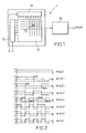
- FIG. 1 The overall structure of an image sensor according to an embodiment of the present invention is shown schematically in FIG. 1.
- This sensor 1 comprises a matrix 10 of photodetector elements intended to receive the light coming from an optical scene to be captured, and to transform the light received into electrical signals.
- a matrix 10 of photodetector elements intended to receive the light coming from an optical scene to be captured, and to transform the light received into electrical signals.
- FIG. 1 only part of the photodetector elements is shown.
- the photodetector elements can in particular be photodiodes or phototransistors.
- the matrix 10 can comprise as many rows as there are columns of photodetector elements.
- the photodetector element Pij located in the ith row and the jth column of a matrix having N rows and N columns, where N is a strictly positive integer and i and j are integers between 0 and N-1, receives a light flux L (i, j) and transforms it into an electric current signal denoted x (i, j).
- the rows of photodetector elements of the matrix 10 are connected to the inputs of a block 12 for generating and storing Walsh functions W (n, i), where n is an integer between 0 and N-1.
- W Walsh functions
- the columns of photodetector elements of the matrix 10 are connected to the inputs of a block 14 for generating and storing Walsh functions W (m, j), where m is an integer between 0 and N- 1.
- W m is an integer between 0 and N- 1.
- the output of a module comprising the matrix 10 of photodetector elements and the blocks 12 and 14 for generating and storing Walsh functions is connected to the input of a module 16 for weighting the electrical signals x (i, j ) by functions calculated from the set of Walsh functions W (n, i) and W (m, j), and summation of the weighted signals.
- the weighting and summing module 16 will be described in more detail below. It outputs NxN Walsh-Hadamard transform coefficients X (n, m) which represent the captured optical scene. The definition and the method of obtaining these coefficients will now be given.
- the optical scene to capture is arbitrary.
- radiometric parameters from the optical scene are measured in the form of NxN electrical signals x (i, j).
- the electrical signal x (i, j) is the collector current
- K (i, j) denotes the photoelectric conversion coefficient of the phototransistor Pij
- ⁇ (i, j) denotes the optical flux coming from the optical scene and picked up by the phototransistor Pij
- In (i, j) represents an intrinsic leakage current in the phototransistor.
- a weighting function Mnm (i, j), called the Walsh-Hadamard mask is generated for each signal x (i, j).
- n and m are integers between 0 and N-1.
- Each mask is worth either +1 or -1.
- FIG. 2 represents, by way of nonlimiting example, the first eight analog Walsh functions with one dimension, as a function of time t, ie W (0, t), W (1, t), ..., W (7, t), on N points.
- each mask can be represented by a checkerboard pattern composed of black portions and white portions.
- the NxN electrical signals x (i, j) are directly weighted by the NxN masks Mnm (i, j ) corresponding and adding the electrical signals thus weighted to obtain NxN Walsh-Hadamard transform coefficients X (n, m), each given by the formula and representing the optical scene captured.
- the electrical signals x (i, j) are weighted by the Mnm masks (i, j) and the summation of the weighted electrical signals by determining a component global positive C + and a global negative component C- of the current, the global positive component C + being the strictly positive sum, according to Kirchhoff's laws, of all the currents x (i, j) having for weighting function a mask Mnm (i , j) worth +1, and the global negative component C- being the strictly positive sum, according to Kirchhoff's laws, of all the currents x (i, j) having for weighting function a mask Mnm (i, j) being equal to -1.
- FIG. 4 is an electrical diagram which illustrates for any couple (n, m) the step which has just been described, namely, the separation of the currents coming from the photodetector elements Pij into two global components positive C + and negative C- .
- the corresponding mask Mnm (i, j) controls the switching of the current x (i, j), i.e. to a line 40 of contribution to the negative global component C-, i.e. towards a line 42 of contribution to the positive global component C +.
- the current x (i, j) comes from the photodetector element Pij, which has been represented diagrammatically in the form of a current generator generating the current x (i, j) and connected to ground.
- the image sensor already described in general with reference to FIG. 1 implements the above method.
- the blocks 12 and 14 and the module 16 of the sensor will now be described in detail, in a particular embodiment.
- FIG. 5A schematically represents the block 12 for generating and storing the N binary values respectively coding the N discrete Walsh functions of order n with one dimension, namely, W (n, i) for all i comprised between 0 and N -1.
- the block 12 comprises p (n) Walsh function generator modules, of identical structure, designated by 52 0 , ..., 52 r-1 , 52 r , ..., 52 p ( n) -1 , arranged in cascade, each having N parallel inputs and N parallel outputs.
- the p (n) modules having an identical structure, only the module 52 r , chosen arbitrarily, will be described in detail.
- 5A represent the arithmetic and logical part of the unit 53 carrying out the operation sgn [cos (K rn .2 r . ⁇ . i / N)] which provides, as described above, the value of f (r, n, i).
- the module 52 r also includes N OR-exclusive operators E r, 0 , ..., E r, N-1 .
- the first inputs of each of these operators are respectively connected to the outputs S r, 0 , ..., S r, N-1 of the calculation unit 53.
- the second inputs of each of the OR-exclusive operators E r, 0 , ..., E r, N-1 are respectively connected to the outputs of the N exclusive-OR operators E r-1,0 , ..., E r-1, N-1 of module 52 r-1 , except in the case of module 52 0 , arranged at the base of the cascade, where the second inputs of each of the exclusive-OR operators are supplied by a logic level "0" of initialization.
- the outputs of the N exclusive-OR operators of the module 52 p (n) -1 are respectively connected to the N inputs of a first suitable conventional digital memory (not shown), for example a ROM, which stores the N bits respectively encoding W ( n, 0), ..., W (n, N-1).
- Figure 5B is similar to Figure 5A. It will therefore only be described briefly. It schematically represents the block 14 for generating and storing the N binary values respectively coding the N discrete Walsh functions of order m with one dimension, namely, W (m, j) for all j between 0 and N-1 .
- Block 14 includes p (m) modules generating Walsh functions, of identical structure, designated by 54 0 , ..., 54 r-1 , 54 r , ..., 54 p (m) -1 , arranged in cascade and connected together in the same way as the modules 52 0 , ..., 52 r-1 , 52 r , ..., 52 p (n) -1 of Figure 5A and having the same structure as them.
- the module 54 r includes a calculation unit 55 which receives as input the bit K r, m defined above and calculates the binary value coding f (r, m, j) for all j between 0 and N-1.
- the second inputs of each of the exclusive-OR operators of the module 54 0 are supplied by a logic level "0" of initialization.
- the outputs of the N exclusive-OR operators of the module 54 p (m) -1 provide the N inputs with a suitable second conventional digital memory (not shown), for example a ROM, the N bits respectively coding W (m, 0), ..., W (m, N-1).
- FIG. 6 represents a part of the overall structure of the image sensor of the invention already illustrated by FIG. 1, in particular the block 12 for generating and storing Walsh functions W (n, i) and the block 14 of generation and memorization of Walsh functions W (m, j).
- FIG. 6 also represents, in an enlarged view, in a particular embodiment, the diagram of an electronic circuit generating a two-dimensional Walsh-Hadamard mask Mnm (i, j) from two discrete Walsh functions at one dimension, let W (n, i) and W (m, j).
- the electronic circuit comprises an OR-exclusive operator 60, whose first input is connected to the output line of block 12 leading to the crossover considered, and whose second input is connected to the output line of block 14 leading to this same crossing.
- the operator 60 therefore performs an OR-exclusive operation between the binary value coding W (n, i) and the binary value coding W (m, j), for a determined value of the couple (i, j), and outputs the binary value coding the mask Mnm (i, j).
- the mask Mnm (i, j) controls the switching of the current x (i, j) so as to provide a contribution to the weighted sum Walsh-Hadamard transform coefficient.
- the electronic diagram of FIG. 7 represents a complex switch 70 formed of a network of NMOS transistors, which simultaneously performs the OR-exclusive operation which has just been described and provides a contribution to the weighted sum of the set masks.
- the complex switch 70 comprises a first group of four NMOS transistors T1, T2, T3, T4.
- the gates of the transistors T1 to T4 are connected to the output of the memory contained in the block 12 for generating and storing Walsh functions W (n, i); the gates of transistors T1 and T2 receive the binary value coding W (n, i), and the gates of transistors T3 and T4 receive the logical inverse of this value, noted W (n, i) ⁇ , which can be achieved very simply by having an inverter at the corresponding output of said memory.
- the complex switch 70 also includes a second group of four NMOS transistors T5, T6, T7, T8.
- the gates of the transistors T5 to T8 are connected to the output of the memory contained in the block 14 for generating and memorizing Walsh functions W (m, j); the gates of transistors T5 and T6 receive the binary value coding W (m, j), and the gates of transistors T7 and T8 receive the logical inverse of this value, ie W (m, d) ⁇ , the reversal can be carried out as described above.
- the drains of the transistors T5 to T8 are connected to the output of the photodetector element Pij, shown in FIG. 7, in a particular embodiment, in the form of a photodiode.
- the drains of the T5 transistors at T8 are supplied by the current x (i, j).
- the sources of the transistors T5, T6, T7, T8 are respectively connected to the drains of the transistors T3, T1, T2, T4.
- the sources of transistors T1 and T3 constitute outputs, denoted "Plus”, of switch 70 where the current x (i, j) is assigned a positive conventional sense, and the sources of transistors T2 and T4 constitute outputs, denoted "Less”, of switch 70 where the current x (i, j) is affected in a negative conventional sense.
- NxN complex switches identical to the one just described are respectively connected to the outputs of block 14. All of these NxN switches form the weighting and summing module 16 mentioned in the description of FIG. 1.
- the image sensor comprises a VLSI circuit which combines the means described above and performs the operations mentioned above in real time.
- the present invention finds a particularly interesting, but not exclusive, application in the field of mobile radiocommunications, for portable devices requiring as low energy consumption as possible and a very small footprint, such as for example in videophone under the GSM standard ( Special Mobile Group). However, it could be used in other fields and in particular those of optical telesurveillance and television.
Applications Claiming Priority (2)
| Application Number | Priority Date | Filing Date | Title |
|---|---|---|---|
| FR9603293A FR2746243B1 (fr) | 1996-03-15 | 1996-03-15 | Procede pour fournir une representation d'une scene optique par transformation de walsh-hadamard et capteur d'image mettant en oeuvre ce procede |
| FR9603293 | 1996-03-15 |
Publications (2)
| Publication Number | Publication Date |
|---|---|
| EP0796006A1 true EP0796006A1 (de) | 1997-09-17 |
| EP0796006B1 EP0796006B1 (de) | 2001-05-30 |
Family
ID=9490227
Family Applications (1)
| Application Number | Title | Priority Date | Filing Date |
|---|---|---|---|
| EP97400577A Expired - Lifetime EP0796006B1 (de) | 1996-03-15 | 1997-03-14 | Verfahren zur Darstellung einer optischen Szene mittels Walsh-Hadamard Transformation und Bildsensor zur Ausführung dieses Verfahrens |
Country Status (5)
| Country | Link |
|---|---|
| US (1) | US5905818A (de) |
| EP (1) | EP0796006B1 (de) |
| JP (1) | JP3834373B2 (de) |
| DE (1) | DE69704976T2 (de) |
| FR (1) | FR2746243B1 (de) |
Cited By (1)
| Publication number | Priority date | Publication date | Assignee | Title |
|---|---|---|---|---|
| US10904049B1 (en) | 2019-07-11 | 2021-01-26 | Stmicroelectronics (Research & Development) Limited | Time domain discrete transform computation |
Families Citing this family (9)
| Publication number | Priority date | Publication date | Assignee | Title |
|---|---|---|---|---|
| DE10160527A1 (de) * | 2001-12-10 | 2003-06-26 | Siemens Ag | Sensoranordnung mit Auslesemitteln zur Differenzbildung |
| KR100597104B1 (ko) | 2004-06-01 | 2006-07-05 | 한국단자공업 주식회사 | 커넥터하우징 |
| US7671321B2 (en) * | 2005-01-18 | 2010-03-02 | Rearden, Llc | Apparatus and method for capturing still images and video using coded lens imaging techniques |
| US20070160308A1 (en) * | 2006-01-11 | 2007-07-12 | Jones Michael J | Difference of sum filters for texture classification |
| TWI360341B (en) * | 2007-11-26 | 2012-03-11 | Univ Nat Kaohsiung Applied Sci | Data encryption method using discrete fractional h |
| RU2638065C2 (ru) * | 2015-12-29 | 2017-12-11 | Общество С Ограниченной Ответственностью "Группа "Магнезит" | Огнеупорное изделие и способ его получения |
| US11895405B2 (en) | 2019-07-12 | 2024-02-06 | University College Cork—National University of Ireland, Cork | Method and system for performing high speed optical image detection |
| WO2023143982A1 (en) * | 2022-01-25 | 2023-08-03 | Sony Semiconductor Solutions Corporation | Solid state imaging device for encoded readout and method of operating |
| WO2024022679A1 (en) * | 2022-07-25 | 2024-02-01 | Sony Semiconductor Solutions Corporation | Solid-state imaging device for encoded readout and method of operating the same |
Citations (7)
| Publication number | Priority date | Publication date | Assignee | Title |
|---|---|---|---|---|
| US3775602A (en) * | 1972-06-29 | 1973-11-27 | Us Air Force | Real time walsh-hadamard transformation of two-dimensional discrete pictures |
| US3925646A (en) * | 1974-04-19 | 1975-12-09 | Battelle Memorial Institute | Information and process control enhancement system employing series of square wave components |
| US4011441A (en) * | 1975-12-22 | 1977-03-08 | General Electric Company | Solid state imaging apparatus |
| US4129887A (en) * | 1977-10-31 | 1978-12-12 | General Electric Company | Solid stage imaging apparatus |
| US4460969A (en) * | 1980-12-04 | 1984-07-17 | The United States Of America As Represented By The Secretary Of The Army | Image spectrum analyzer for cartographic feature extraction |
| US4590608A (en) * | 1980-05-30 | 1986-05-20 | The United States Of America As Represented By The Secretary Of The Army | Topographic feature extraction using sensor array system |
| US5262871A (en) * | 1989-11-13 | 1993-11-16 | Rutgers, The State University | Multiple resolution image sensor |
Family Cites Families (7)
| Publication number | Priority date | Publication date | Assignee | Title |
|---|---|---|---|---|
| US4261043A (en) * | 1979-08-24 | 1981-04-07 | Northrop Corporation | Coefficient extrapolator for the Haar, Walsh, and Hadamard domains |
| JPS5737925A (en) * | 1980-08-14 | 1982-03-02 | Matsushita Electric Ind Co Ltd | High-speed hadamard converter |
| US4335373A (en) * | 1980-11-07 | 1982-06-15 | Fairchild Camera & Instrument Corp. | Method for analyzing a digital-to-analog converter with a nonideal analog-to-digital converter |
| EP0128298B1 (de) * | 1983-04-11 | 1990-07-04 | Nec Corporation | Orthogonale Transformation und Gerät zu ihrer Durchführung |
| US4809194A (en) * | 1986-08-28 | 1989-02-28 | Hughes Aircraft Company | Image processing system and method using modulated detector outputs |
| US5175802A (en) * | 1986-08-28 | 1992-12-29 | Hughes Aircraft Company | Macro image processing system |
| US4892370A (en) * | 1987-03-09 | 1990-01-09 | Lee Yun Parn T | Means and method for implementing a two-dimensional truth-table look-up holgraphic processor |
-
1996
- 1996-03-15 FR FR9603293A patent/FR2746243B1/fr not_active Expired - Lifetime
-
1997
- 1997-03-14 EP EP97400577A patent/EP0796006B1/de not_active Expired - Lifetime
- 1997-03-14 DE DE69704976T patent/DE69704976T2/de not_active Expired - Lifetime
- 1997-03-17 JP JP06363697A patent/JP3834373B2/ja not_active Expired - Fee Related
- 1997-03-17 US US08/818,945 patent/US5905818A/en not_active Expired - Fee Related
Patent Citations (7)
| Publication number | Priority date | Publication date | Assignee | Title |
|---|---|---|---|---|
| US3775602A (en) * | 1972-06-29 | 1973-11-27 | Us Air Force | Real time walsh-hadamard transformation of two-dimensional discrete pictures |
| US3925646A (en) * | 1974-04-19 | 1975-12-09 | Battelle Memorial Institute | Information and process control enhancement system employing series of square wave components |
| US4011441A (en) * | 1975-12-22 | 1977-03-08 | General Electric Company | Solid state imaging apparatus |
| US4129887A (en) * | 1977-10-31 | 1978-12-12 | General Electric Company | Solid stage imaging apparatus |
| US4590608A (en) * | 1980-05-30 | 1986-05-20 | The United States Of America As Represented By The Secretary Of The Army | Topographic feature extraction using sensor array system |
| US4460969A (en) * | 1980-12-04 | 1984-07-17 | The United States Of America As Represented By The Secretary Of The Army | Image spectrum analyzer for cartographic feature extraction |
| US5262871A (en) * | 1989-11-13 | 1993-11-16 | Rutgers, The State University | Multiple resolution image sensor |
Non-Patent Citations (1)
| Title |
|---|
| FALKOWSKI B J: "GENERALIZED WALSH TRANSFORMS OF BOOLEAN FUNCTIONS", PROCEEDINGS OF THE INTERNATIONAL SYMPOSIUM ON CIRCUITS AND SYSTEMS, SAN DIEGO, MAY 10 - 13, 1992, vol. 1 OF 6, 10 May 1992 (1992-05-10), INSTITUTE OF ELECTRICAL AND ELECTRONICS ENGINEERS, pages 137 - 140, XP000337262 * |
Cited By (1)
| Publication number | Priority date | Publication date | Assignee | Title |
|---|---|---|---|---|
| US10904049B1 (en) | 2019-07-11 | 2021-01-26 | Stmicroelectronics (Research & Development) Limited | Time domain discrete transform computation |
Also Published As
| Publication number | Publication date |
|---|---|
| JP3834373B2 (ja) | 2006-10-18 |
| FR2746243B1 (fr) | 1998-06-05 |
| DE69704976T2 (de) | 2002-04-04 |
| FR2746243A1 (fr) | 1997-09-19 |
| DE69704976D1 (de) | 2001-07-05 |
| JPH1056386A (ja) | 1998-02-24 |
| EP0796006B1 (de) | 2001-05-30 |
| US5905818A (en) | 1999-05-18 |
Similar Documents
| Publication | Publication Date | Title |
|---|---|---|
| Yang et al. | Bits from photons: Oversampled image acquisition using binary poisson statistics | |
| FR2679722A1 (fr) | Processeur destine a generer une transformee de walsh. | |
| EP0206847B1 (de) | Rechnungseinrichtungen von Cosinustransformationen, solche Rechnungseinrichtungen enthaltende Kodierungs- und Dekodierungseinrichtung von Bildern | |
| EP0796006B1 (de) | Verfahren zur Darstellung einer optischen Szene mittels Walsh-Hadamard Transformation und Bildsensor zur Ausführung dieses Verfahrens | |
| FR2555377A1 (fr) | Circuit electronique utilisable dans les dispositifs a circuit integre contenant des filtres a condensateurs commutes | |
| FR2697704A1 (fr) | Procédé et dispositif de segmentation en sous-bandes et de reconstruction d'un signal numérique, et dispositif correspondant. | |
| FR2738364A1 (fr) | Procede et processeur de transformation cosinusoidale discrete inverse | |
| EP0262032B1 (de) | Binärer Addierer mit festem Operand und paralleler/serieller Multiplikator mit solchen Addierern | |
| FR2667176A1 (fr) | Procede et circuit de codage d'un signal numerique pour determiner le produit scalaire de deux vecteurs et traitement tcd correspondant. | |
| EP0022513B1 (de) | Gerät zur Berechnung der zweidimensionalen diskreten Fouriertransformation | |
| EP0536062B1 (de) | Verfahren und Vorrichtung zur Datenverarbeitung mittels Kosinustransformation | |
| EP0206892A1 (de) | Verarbeitungsverfahren für ein ursprüngliches Bild darstellende digitale Signale | |
| EP0691065B1 (de) | Kompatible teilbandkodierung/dekodierung von fernsehbildern | |
| EP1324210A1 (de) | Einrichtung zur inversen adaptiven Transformation | |
| FR2625399A1 (fr) | Dispositif de regulation de debit conjointe a au moins deux composantes de signaux video numeriques | |
| EP2327218B1 (de) | Verfahren zum entropischen transkodieren eines ersten binärdatenstroms zu einem zweiten komprimierten binärdatenstrom und entsprechendes computerprogramm und bildaufzeichnungsgerät | |
| FR2680292A1 (fr) | Filtre bidimensionnel a reponse impulsionnelle finie. | |
| EP0603070B1 (de) | Verfahren und Vorrichtung zur analogen Bildfaltung | |
| EP0667680A1 (de) | Verfahren und Vorrichtung zur vektoriellen Quantifizierung eines digitalen Signals, insbesondere geeignet zur Komprimierung von digitalen Bildern | |
| FR2521322A1 (fr) | Circuit de traitement de signaux numeriques notamment un circuit travaillant a vitesse faible | |
| FR2844129A1 (fr) | Procede et capteur pour determiner le contraste local d'une scene observee, par detection de la luminance emanant de cette scene | |
| FR2536541A1 (fr) | Systeme simplifie d'analyse spectrale a exploitation de phase | |
| EP0329572B1 (de) | Binärzahlmultiplizierer mit einer sehr grossen Bitzahl | |
| EP0376769B1 (de) | Vorrichtung zur Zeile-Spalte-Matrixtransponierung mit Schieberegistern und Umschaltern | |
| BE899986A (fr) | Appareil de traitement de signaux en pyramide hierarchique en temps reel. |
Legal Events
| Date | Code | Title | Description |
|---|---|---|---|
| PUAI | Public reference made under article 153(3) epc to a published international application that has entered the european phase |
Free format text: ORIGINAL CODE: 0009012 |
|
| AK | Designated contracting states |
Kind code of ref document: A1 Designated state(s): DE GB |
|
| 17P | Request for examination filed |
Effective date: 19980113 |
|
| 17Q | First examination report despatched |
Effective date: 19991124 |
|
| GRAG | Despatch of communication of intention to grant |
Free format text: ORIGINAL CODE: EPIDOS AGRA |
|
| RTI1 | Title (correction) |
Free format text: METHOD OF PROVIDING A REPRESENTATION OF AN OPTICAL SCENE BY THE WALSH-HADAMARD TRANSFORM AND AN IMAGE SENSOR IMPLEMENTING THE METHOD |
|
| GRAG | Despatch of communication of intention to grant |
Free format text: ORIGINAL CODE: EPIDOS AGRA |
|
| GRAH | Despatch of communication of intention to grant a patent |
Free format text: ORIGINAL CODE: EPIDOS IGRA |
|
| GRAH | Despatch of communication of intention to grant a patent |
Free format text: ORIGINAL CODE: EPIDOS IGRA |
|
| GRAA | (expected) grant |
Free format text: ORIGINAL CODE: 0009210 |
|
| AK | Designated contracting states |
Kind code of ref document: B1 Designated state(s): DE GB |
|
| REF | Corresponds to: |
Ref document number: 69704976 Country of ref document: DE Date of ref document: 20010705 |
|
| GBT | Gb: translation of ep patent filed (gb section 77(6)(a)/1977) |
Effective date: 20010824 |
|
| REG | Reference to a national code |
Ref country code: GB Ref legal event code: IF02 |
|
| PLBE | No opposition filed within time limit |
Free format text: ORIGINAL CODE: 0009261 |
|
| STAA | Information on the status of an ep patent application or granted ep patent |
Free format text: STATUS: NO OPPOSITION FILED WITHIN TIME LIMIT |
|
| 26N | No opposition filed | ||
| REG | Reference to a national code |
Ref country code: GB Ref legal event code: 732E Free format text: REGISTERED BETWEEN 20090528 AND 20090603 |
|
| PGFP | Annual fee paid to national office [announced via postgrant information from national office to epo] |
Ref country code: GB Payment date: 20160224 Year of fee payment: 20 |
|
| PGFP | Annual fee paid to national office [announced via postgrant information from national office to epo] |
Ref country code: DE Payment date: 20160324 Year of fee payment: 20 |
|
| REG | Reference to a national code |
Ref country code: DE Ref legal event code: R071 Ref document number: 69704976 Country of ref document: DE |
|
| REG | Reference to a national code |
Ref country code: GB Ref legal event code: PE20 Expiry date: 20170313 |
|
| PG25 | Lapsed in a contracting state [announced via postgrant information from national office to epo] |
Ref country code: GB Free format text: LAPSE BECAUSE OF EXPIRATION OF PROTECTION Effective date: 20170313 |