EP0794688B1 - Capped edge emitter - Google Patents
Capped edge emitter Download PDFInfo
- Publication number
- EP0794688B1 EP0794688B1 EP97301377A EP97301377A EP0794688B1 EP 0794688 B1 EP0794688 B1 EP 0794688B1 EP 97301377 A EP97301377 A EP 97301377A EP 97301377 A EP97301377 A EP 97301377A EP 0794688 B1 EP0794688 B1 EP 0794688B1
- Authority
- EP
- European Patent Office
- Prior art keywords
- cap
- film
- radiation
- edge emitter
- active film
- Prior art date
- Legal status (The legal status is an assumption and is not a legal conclusion. Google has not performed a legal analysis and makes no representation as to the accuracy of the status listed.)
- Expired - Lifetime
Links
- 239000010408 film Substances 0.000 claims description 108
- 230000005855 radiation Effects 0.000 claims description 64
- 239000010409 thin film Substances 0.000 claims description 15
- 230000005540 biological transmission Effects 0.000 claims description 13
- 230000001902 propagating effect Effects 0.000 claims description 6
- 239000005387 chalcogenide glass Substances 0.000 claims description 5
- CJOBVZJTOIVNNF-UHFFFAOYSA-N cadmium sulfide Chemical compound [Cd]=S CJOBVZJTOIVNNF-UHFFFAOYSA-N 0.000 claims description 3
- 229910052980 cadmium sulfide Inorganic materials 0.000 claims description 3
- 238000000034 method Methods 0.000 description 17
- XLOMVQKBTHCTTD-UHFFFAOYSA-N Zinc monoxide Chemical compound [Zn]=O XLOMVQKBTHCTTD-UHFFFAOYSA-N 0.000 description 10
- 239000000463 material Substances 0.000 description 8
- 230000000694 effects Effects 0.000 description 6
- 239000002019 doping agent Substances 0.000 description 5
- 238000005401 electroluminescence Methods 0.000 description 5
- 230000003287 optical effect Effects 0.000 description 5
- 239000011787 zinc oxide Substances 0.000 description 5
- 238000010586 diagram Methods 0.000 description 4
- 229910052751 metal Inorganic materials 0.000 description 4
- 239000002184 metal Substances 0.000 description 4
- 239000000758 substrate Substances 0.000 description 4
- 229910052782 aluminium Inorganic materials 0.000 description 3
- XAGFODPZIPBFFR-UHFFFAOYSA-N aluminium Chemical compound [Al] XAGFODPZIPBFFR-UHFFFAOYSA-N 0.000 description 3
- 239000006117 anti-reflective coating Substances 0.000 description 3
- 239000011248 coating agent Substances 0.000 description 3
- 238000000576 coating method Methods 0.000 description 3
- 230000005684 electric field Effects 0.000 description 3
- 239000011521 glass Substances 0.000 description 3
- 230000008569 process Effects 0.000 description 3
- VYPSYNLAJGMNEJ-UHFFFAOYSA-N Silicium dioxide Chemical compound O=[Si]=O VYPSYNLAJGMNEJ-UHFFFAOYSA-N 0.000 description 2
- 230000002238 attenuated effect Effects 0.000 description 2
- 229910001610 cryolite Inorganic materials 0.000 description 2
- 230000005284 excitation Effects 0.000 description 2
- 150000002500 ions Chemical class 0.000 description 2
- 230000000149 penetrating effect Effects 0.000 description 2
- 238000007788 roughening Methods 0.000 description 2
- ZAMOUSCENKQFHK-UHFFFAOYSA-N Chlorine atom Chemical compound [Cl] ZAMOUSCENKQFHK-UHFFFAOYSA-N 0.000 description 1
- GYHNNYVSQQEPJS-UHFFFAOYSA-N Gallium Chemical compound [Ga] GYHNNYVSQQEPJS-UHFFFAOYSA-N 0.000 description 1
- PWHULOQIROXLJO-UHFFFAOYSA-N Manganese Chemical compound [Mn] PWHULOQIROXLJO-UHFFFAOYSA-N 0.000 description 1
- XUIMIQQOPSSXEZ-UHFFFAOYSA-N Silicon Chemical compound [Si] XUIMIQQOPSSXEZ-UHFFFAOYSA-N 0.000 description 1
- 239000005083 Zinc sulfide Substances 0.000 description 1
- 230000009471 action Effects 0.000 description 1
- 238000004458 analytical method Methods 0.000 description 1
- 230000001174 ascending effect Effects 0.000 description 1
- 229910052801 chlorine Inorganic materials 0.000 description 1
- 239000000460 chlorine Substances 0.000 description 1
- 230000008878 coupling Effects 0.000 description 1
- 238000010168 coupling process Methods 0.000 description 1
- 238000005859 coupling reaction Methods 0.000 description 1
- 238000009826 distribution Methods 0.000 description 1
- 230000005670 electromagnetic radiation Effects 0.000 description 1
- 229910052733 gallium Inorganic materials 0.000 description 1
- 238000003384 imaging method Methods 0.000 description 1
- 230000006872 improvement Effects 0.000 description 1
- 229910052738 indium Inorganic materials 0.000 description 1
- APFVFJFRJDLVQX-UHFFFAOYSA-N indium atom Chemical compound [In] APFVFJFRJDLVQX-UHFFFAOYSA-N 0.000 description 1
- AMGQUBHHOARCQH-UHFFFAOYSA-N indium;oxotin Chemical compound [In].[Sn]=O AMGQUBHHOARCQH-UHFFFAOYSA-N 0.000 description 1
- 238000004020 luminiscence type Methods 0.000 description 1
- 229910052748 manganese Inorganic materials 0.000 description 1
- 239000011572 manganese Substances 0.000 description 1
- 238000004519 manufacturing process Methods 0.000 description 1
- 238000001465 metallisation Methods 0.000 description 1
- 238000005498 polishing Methods 0.000 description 1
- 230000006798 recombination Effects 0.000 description 1
- 238000005215 recombination Methods 0.000 description 1
- 238000002310 reflectometry Methods 0.000 description 1
- 238000005488 sandblasting Methods 0.000 description 1
- 229910052710 silicon Inorganic materials 0.000 description 1
- 239000010703 silicon Substances 0.000 description 1
- 235000012239 silicon dioxide Nutrition 0.000 description 1
- 239000000377 silicon dioxide Substances 0.000 description 1
- DRDVZXDWVBGGMH-UHFFFAOYSA-N zinc;sulfide Chemical compound [S-2].[Zn+2] DRDVZXDWVBGGMH-UHFFFAOYSA-N 0.000 description 1
Images


Classifications
-
- B—PERFORMING OPERATIONS; TRANSPORTING
- B41—PRINTING; LINING MACHINES; TYPEWRITERS; STAMPS
- B41J—TYPEWRITERS; SELECTIVE PRINTING MECHANISMS, i.e. MECHANISMS PRINTING OTHERWISE THAN FROM A FORME; CORRECTION OF TYPOGRAPHICAL ERRORS
- B41J2/00—Typewriters or selective printing mechanisms characterised by the printing or marking process for which they are designed
- B41J2/435—Typewriters or selective printing mechanisms characterised by the printing or marking process for which they are designed characterised by selective application of radiation to a printing material or impression-transfer material
- B41J2/447—Typewriters or selective printing mechanisms characterised by the printing or marking process for which they are designed characterised by selective application of radiation to a printing material or impression-transfer material using arrays of radiation sources
- B41J2/45—Typewriters or selective printing mechanisms characterised by the printing or marking process for which they are designed characterised by selective application of radiation to a printing material or impression-transfer material using arrays of radiation sources using light-emitting diode [LED] or laser arrays
-
- H—ELECTRICITY
- H05—ELECTRIC TECHNIQUES NOT OTHERWISE PROVIDED FOR
- H05B—ELECTRIC HEATING; ELECTRIC LIGHT SOURCES NOT OTHERWISE PROVIDED FOR; CIRCUIT ARRANGEMENTS FOR ELECTRIC LIGHT SOURCES, IN GENERAL
- H05B33/00—Electroluminescent light sources
- H05B33/02—Details
- H05B33/04—Sealing arrangements, e.g. against humidity
-
- H—ELECTRICITY
- H05—ELECTRIC TECHNIQUES NOT OTHERWISE PROVIDED FOR
- H05B—ELECTRIC HEATING; ELECTRIC LIGHT SOURCES NOT OTHERWISE PROVIDED FOR; CIRCUIT ARRANGEMENTS FOR ELECTRIC LIGHT SOURCES, IN GENERAL
- H05B33/00—Electroluminescent light sources
- H05B33/12—Light sources with substantially two-dimensional radiating surfaces
- H05B33/26—Light sources with substantially two-dimensional radiating surfaces characterised by the composition or arrangement of the conductive material used as an electrode
- H05B33/28—Light sources with substantially two-dimensional radiating surfaces characterised by the composition or arrangement of the conductive material used as an electrode of translucent electrodes
Definitions
- the present invention relates generally to light generated by electroluminescence, and particularly to edge emitters emitting light generated by electroluminescence.
- an edge emitter emitting light through electroluminescence has a structure with multiple films, known as a thin film electroluminescent stack.
- the stack typically includes five films, a conductive electrode, an insulating film, an active film, another insulating film and another electrode.
- the basic idea is to excite dopant ions in the active film. When the excited dopants relax, light is generated. The potential difference between the top and the bottom electrodes creates electric fields for excitation.
- the insulating films and the active film are typically built as a sheet, with the top and the bottom electrodes as stripes E1 and E2.
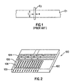
- Figure 1 shows a representation of the top view of this structure. The intersection of the two stripes defines a pixel.
- the pixel has a length of I and a width of w.
- the width w is much smaller than the length I.
- the film stack is fabricated so that one of the width side is exposed to form the edge of the edge emitter. The idea is to have a large area generating light, and a small edge to define the size of a small beam of emitted light.
- the edge emitter is used for the print head of a 600 dots-per-inch (dpi) printer, there should be more than 5000 pixels on a line, one adjacent to the other. Each pixel is responsible for one dot of the printer. In such an embodiment, the width of each dot is about 0.035mm. Based on a pixel length of 3 mm and common edge emitter materials, a light power of 20,000 nW can be generated under each pixel. Although the power generated is high, probably, only about 70 nW will be coupled out through the edge. This gives a 0.35% optical efficiency.
- One approach to increase the optical output is to increase the area of the pixel to generate more light. To keep the light beam from the edge small, the width has to be small. Therefore, the way to increase the area is to increase the length of the pixel.
- the film stack has attenuation. Measured attenuation lengths of a typical film stack lie in the range of 0.07 to 0.5 mm. Further increasing the length of a pixel will not increase the power emitted.
- the present invention provides an edge emitter with significantly higher optical efficiency. Based on the present invention, a significantly higher percentage of light generated by each pixel is directed towards its corresponding edge.
- the present invention incorporates a cap on top of a thin film electroluminescent stack.
- the cap gathers, re-directs and guides a significant portion of the generated radiation into the direction of the edge of the edge emitter.
- the thin film electroluminescent stack includes a top transparent electrode, a bottom electrode, an active film between the two electrodes, and an insulating layer between the active film and the bottom electrode. Note that as compared to conventional thin film stack, the thin film stack of the present invention does not have an insulating film between the active film and the top transparent electrode.
- the cap preferably thicker than the thin film stack, is made of a material with a lower attenuation than the film stack. Both the refractive indexes of the cap and the top transparent electrode are substantially matched to the refractive index of the active film to increase the amount of electroluminescent radiation propagating from the active film into the cap.
- the present invention successfully identifies appropriate transparent electrodes; this is a challenging task all by itself.
- the cap has a number of side surfaces and a top surface, with the transmission coefficient of one side surface, known as the emitting side surface, being higher than the transmission coefficient of at least one other surface, known as the reflecting surface.
- the top surface and all the side surfaces of the cap, except the emitting side surface are smooth and reflecting surfaces.
- the emitting side surface is tilted to increase the amount of generated radiation to be emitted from the emitting side surface.
- the edge emitter can be further improved by controlling the thickness of the insulating film to be within a predetermined range.
- Figure 1 shows the top view of a prior art edge emitter.
- Figure 2 shows a system with an array of preferred edge emitters of the present invention.
- Figures 3A-C show cross-sections of preferred edge emitters of the present invention.
- Figure 4 shows another preferred embodiment increasing the re-directions of light by the top surface.
- Figure 5 shows a ray diagram comparing the paths of the generated radiation between the prior art and one cross section of the preferred embodiment of the present invention.
- Figure 6 shows a ray diagram comparing the paths of the generated radiation between the prior art and another cross section of the preferred embodiment of the present invention.
- Figure 7 shows the effect of mismatch between the active film and the electrodes in the present invention.
- Figure 8 shows the percentage of power reflected versus the incident angle for different types of the transparent electrodes in the present invention.
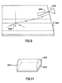
- Figure 9 shows tilting the emitting side surface in the present invention.
- Figure 10 shows the percentage of power reflected by the reflective electrode as a function of incident angle for different thicknesses of the insulating film in the present invention.
- Figure 11 shows a different preferred embodiment of the present invention.
- Figure 12 shows another preferred embodiment of the present invention.
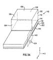
- FIG. 2 shows a system 100 with an array 106 of preferred edge emitters, such as 108, of the present invention.
- the array 106 is typically on a substrate 102, such as glass.
- the system also shows multiplexing bus bars 104 connecting drivers to the edge emitters.
- the driver with multiplexers 104 will not be further described because they should be obvious to those skilled in the art.
- each edge emitter would emit an electromagnetic radiation, such as the emitter 108 emitting the radiation 109.
- FIG 3A shows a cross-section of a first preferred embodiment of an edge emitter 110.
- the emitter is made of a cap 112 situated on top of a thin film electroluminescent stack to form a modified edge emitter--hereinafter known as an edge emitter.
- the thin film electroluminescent stack includes a transparent electrode 114; an active film 118; an insulating film 120; and a reflective electrode 122.
- the electrodes are conductive. Unlike conventional stacks, the stack in the present invention does not have an insulating film between the active film and the transparent electrode.
- Electric fields are applied across the active film 118, such as by connecting a voltage source 124 on the two electrodes.
- the electric field across the active film excites dopant ions in the active film 118; and then the excited dopants relax to generate radiation.
- the fabrication processes of the preferred embodiments will not be described because such processes should be obvious to those skilled in the art.
- the preferred embodiment 110 shows the transparent and the reflective electrodes well registered, with one directly on top of the other.
- one electrode can be much wider than another. It is only in the regions of overlap that there will be excitation and recombination.
- the reflective electrode 122, the insulating film 120 and the transparent electrode 114 are quite thin; the active film 118 is thicker, but the cap 112 is even thicker than the active film.
- the insulating film 120 on top of the reflective electrode fills in the gap between adjacent reflective electrodes, such as in the region 140.
- the reflective electrode 122 is much wider than the transparent electrode 114.
- Materials for the cap should be selected according to their electromagnetic properties. This includes their refractive indexes, which should be similar to the index of the active film so as to enhance coupling of the radiation generated in the active film 118 into the cap 112.
- the cap should be made of a material with less attenuation per unit length of the generated radiation than the active film 118. Other factors to consider are the manufacturability of the cap on the transparent electrode in the desired dimensions. This includes the achievable smoothness of the surfaces, which is important, as will be explained.
- the cap 112 has four side surfaces 132, 134, 136, 138, and a top surface 130.
- radiation is directed to go out from one of the side surfaces (the emitting side surface 132) and from the edge 142 of the active film 118.
- the radiation preferably emits along the x-direction.
- the emitting side surface 132 is made to have a higher transmission than the other side surfaces (the reflecting side surfaces 134, 136 and 138) and the top surface 130.
- Figure 3B shows another preferred embodiment 150 of the present invention. It shows two capped structures, 152 and 154.
- the reflective electrode 156 is common for both structures.
- each cap structure has its own transparent electrode, such as the cap 154 has the transparent electrode 158, and the cap 152 has the electrode 162.
- a first method is to have a smooth top surface and reflecting side surfaces; optically, this means that those surfaces have high finesse.
- the emitting side surface is roughened, such as by sandblasting it. Roughening a surface to increase its transmission or radiation emission, and polishing a surface to decrease its transmission are taught in prior art references, such as "ZnSiMn in Polycrystalline Electroluminescence Thin Film Display,” published by Mach and Mueller in the J. Cryst. Growth 86, pages 866-872 in 1988, and "The Counterplay between Brightness and Contrast in Electroluminescence Devices,” published by Mach et al. in J. Luminescence 40/41, pages 779-781 in 1988.
- a second method is to cover the top surface and the reflecting side surfaces with metal films, for example, as shown in Figure 3C.
- a third method is to coat a film of material with a refractive index much lower than that of the cap on the cap's reflecting side surfaces and top surface. The mismatch in refractive indexes reflect incident radiation on those surfaces.
- a fourth method combines the second and the third method by first forming the low refractive index material on those surfaces and then covering them with metal films. Sometimes, it might be preferable to ignore the edge 142 of the active film 118, and focus on the emitting side surface 132, especially when the cap is much thicker than the active film. Note, also, that the emitting side surface 132 of the cap may not have to coincide with the edge 142 of the stack; it may extend beyond the edge. This may improve the ease in manufacturability of the edge emitter.
- Figure 4 shows another preferred embodiment of the present invention showing a fifth method to increase the re-direction of light by the top surface.
- the top surface 170 of a cap 172 is grooved to redirect light penetrating through the transparent electrode 174 of a thin film electroluminescent stack under small angles towards the emitting side surface 176. If the top surface is just smoothed, without other enhancement on its reflectivity, most of the incident radiation, except those within a cone, will still be reflected.
- the angle of the cone is the critical angle of the cap material.
- a cap material with refractive index of 2.3 would reflect about 90% of the incident light.
- the grooved structure further redirects a significant portion of the radiation within the cone towards the emitting side surface.
- the ascending angle 180 of a groove is about 10 degrees, and the descending angle of the groove is about 45 degrees.
- the methods to generate such grooves should be well known to those skilled in the art.
- Figure 5 shows a ray diagram comparing the paths of the generated radiation between the prior art and one perspective of the preferred embodiment 110 of the present invention.
- the perspective is a cross-section parallel to the reflecting side surface 134.
- radiation generated at 200 is directed across the active film 118 before it is radiated out of the edge emitter 110.
- the guiding is done through numerous total internal reflections, as shown by the path 202.
- the cap In the present invention, most of the radiation generated at 200 propagates to the cap 112.
- the cap is thicker than the active film 118. This leads to fewer total internal reflections before the radiation hits the emitting side surface 132.
- radiation generated 200 follows the path 204 with one total internal reflection before it goes out of the emitting side surface 132.
- the attenuation of the radiation per unit length in the cap 112 is less than that in the active film 118.
- a higher percentage of the light generated radiates out of the emitter 110.
- a thicker cap improves the guiding of the radiation towards the emitting side surface by reducing the number of total internal reflection.
- the cap should not be too thick. This is because a thick cap increases the size of the beam of radiation coming out of the emitter.
- Figure 6 shows a ray diagram comparing the paths of the generated radiation between the prior art and another perspective of the preferred embodiment 110 of the present invention. This perspective is the cross-section parallel to the emitting side surface 132.
- radiation generated at 250 is guided along the plane of the active film through the path 252 by numerous total internal reflections. Such radiation just propagates along the thin film electroluminescent stack; it is typically significantly attenuated and will not radiate from the edge 142 of the active film 118.
- the radiation generated substantially follows the path 254 in the cap.
- the emitting side surface is preferably more transmissive than all the side surfaces and the top surface. As long as the radiation path 254 is not absolutely parallel to the emitting side surface 132, ultimately, if the radiation is not attenuated, the radiation would go out of the emitting side surface 132. This is achieved by internal reflections along "spiraling" paths.
- the refractive indices of the cap 112 and the transparent electrode 114 is substantially matched to the refractive index of the active film 118 to reduce the effect of mismatch and to increase the amount of radiation propagating from the active film 118 into the cap 112.
- a thin film electroluminescent stack has an additional insulating film between the transparent electrode and the active film.
- that insulating film is removed to reduce interface-reflections.
- the effect of mismatch at the active-film-and-the-removed-insulating-film interface and the effect of mismatch at the removed-insulating-film-and-the-transparent-electrode interface is not significant. This is because the removed insulating film and the transparent electrode are typically very thin with respect to the wavelength of the radiation emitted from the emitter.
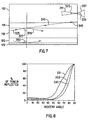
- Figure 7 shows the effect of mismatch between the active film and the electrodes, when the incident angle of the radiation at an interface is large.
- the preferred incident angle may be quite large in the same embodiments of the present invention; and with a large incident angle, a mismatch in refractive indexes becomes significant.
- the typical insulating film between the transparent electrode and the active film is removed, and the refractive index of the transparent electrode is taken into consideration.
- the curve 331 represents a transparent electrode using an ITO of 100nm thick; the curve 333 represents a transparent electrode using a ZnO layer of 100nm thick; and the curve 335 represents a transparent electrode using a ZnO layer of 80nm thick. As the incident angle increases, the percentage of power reflected back into the active layer increases.
- the incident angle 327 should be as high as or even higher than 80 degrees. This is because typically, the emitting side surface is optically coupled to a lens to focus the emitted radiation.
- the lens has an F-number of 1, implying the radiation that can be coupled into the lens has to be confined within an acceptance cone 337 with an acceptance angle 339 of about +/- 20 degrees.
- the refractive index of the cap is 2.3, based on Snell's law, the cap cone 341 of radiation from the cap that falls within the acceptance cone 337 is limited to a cap angle 343 of about +/- 8.5 degrees.
- the lens will not accept any radiation 345 incident to the emitting side surface that has an incident angle on the emitting side surface larger than 8.5 degrees.
- the incident angle 327 on the transparent electrode 114 interface should preferably be as high as or even higher than 80 degrees for the lens to capture the emitted radiation.
- the transparent-layer-active-film interface reflects 60% of the incident power in every reflection.
- the present invention has removed the insulating film between the transparent electrode and the active film.
- the refractive indices of the cap and the transparent electrode are substantially matched to the refractive index of the active film to reduce the amount of power reflected at the active-film-transparent-electrode interface, and at the transparent-electrode-cap interface.
- substantially matched is defined as having both the refractive indexes of the cap and the transparent electrode being within about +/- 10% of the refractive index of the active film.
- the desired incident angle 327 may be more than 80 degrees. At those incident angles, the percentage of power reflected is high. As shown in Figure 8, one way to reduce the percentage of power reflected is to reduce the magnitude of the incident angle 327.
- FIG. 9 shows tilting the emitting side surface by an angle 340, such as 15 degrees.
- the acceptance cone 342 and the cap cone 344 remain the same as before the tilt, but in terms of orientation, they are also tilted by the same angle 340.
- the desired incident angles 346 or the incident angles of the generated radiation that fall into the acceptance cone 342 will be reduced by the tilt angle 340.
- a lower incident angle reduces the percentage of power reflected at the active-film-transparent-electrode interface when the index of the active film is not perfectly matched to the index of the transparent electrode.
- the present invention can be further improved by confining the thickness of the insulating film 120 to be within certain ranges. Again this is due to the acceptance cone discussed above.
- the insulating film should be very thin, if the insulating film is too thin, the results may not be as desirable.
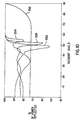
- Figure 10 shows the percentage of power reflected by an aluminum reflective electrode of about 100 to 200 nanometers thick as a function of incident angle 350 on the reflective electrode 122 for different thicknesses of the insulating film.
- the curve 352 represents the reflected power for an emitted radiation at 800 nanometer with an extremely thin insulating film 120 -- the insulating film has practically zero thickness; the other curves represent the reflected power for an insulating film of silicon oxynitride that is about 360 nanometers thick with the emitted radiation at 550 nanometers (354), 650 nanometers (356) and 800 nanometers (358) respectively.
- curve 352 shows that for the reflective electrode to be 100% reflective, the incident angle 350 has to be close to 90 degrees. As explained above, due to the acceptance cone, the desired incident angle of concern can be quite large, but do not have to be almost 90 degrees.
- the amount of power reflected by the reflecting electrode is practically 100% for radiation equal to or more than 550 nanometers, even if the incident angle 350 on the reflective electrode is just more than 70 degrees.
- the thickness of the insulating film is controlled to increase the amount of radiation reflected from the reflective electrode back into the active film.
- the reflecting electrode 122 is made of aluminum.
- the insulating film is made of siliconoxinitride, with a refractive index of about 1.7.
- the active film is made of zinc sulphide doped with manganese.
- the refractive index of the active film is about 2.3.
- the transparent electrode is made of cadmium sulphide that has a refractive index also between 2.3 and 2.4. To make the cadmium sulphide conducting, it is doped by one of the following elements: chlorine, gallium and indium. The range of dopant is preferably between 0.02 and 0.6 atomic percent.
- the cap is made of a Chalcogenide glass that has a refractive index between 2.1 and 2.5.
- Chalcogenide glass A number of ways may be used to fabricate the Chalcogenide glass; one example is shown in publication titled, "Index of Refraction and D.C. Electrical Conducting in Ge 40-x Sb x S 60 Glasses," published by Tichi et al., in the Czech J. Phys. B32, pages 1363-1373, in 1982, teaching how to build Chalcogenide glasses with refractive indices that are in the range of 2.3 to 2.6.
- the transparent electrode is a part of the cap; for example, both are made of Chalcogenide glass, with the transparent electrode portion of the glass being doped to make it conducting.
- the reflecting electrode has a thickness (y-direction) of about 100 to 200 nanometers; the insulating film has the thickness of about 300 to 400 nanometers; the active film is about 1 micron thick; and the transparent electrode is about 200 nanometers thick.
- the cap is about 10 microns thick (y-direction), 0.04 mm wide (z-direction) and 3 mm long (x-direction).
- the reflecting side surfaces and the top surface are covered by aluminum with a thickness of about 1000 Angstroms.
- the reflective performance can be further improved if there is a film with a refractive index lower than that of the cap, such as cryolite, between the cap and the metal surface.
- Cryolite has a refractive index of 1.33.
- the electroluminescent radiation is yellow, with a wavelength of 600 nm.
- the optical efficiency of the above structure increases by about 1000% as compared to a similar structure with the additional insulating film between the transparent film and the active film, without the cap 112, without the matched refractive indexes and without the controlled insulating film thickness.
- the reflective electrode does not have to be reflective.
- the edge emitter may not be as efficient because some of the radiation propagate through the "reflective electrode.”
- the present invention describes the emitting side surface having a higher transmission than the other side surfaces.
- the emitting side surface has a higher transmission than at least one side surface, such as the surface 136, which is directly opposite to the emitting surface 132 in Figure 3A. This is achieved, for example, by roughening the emitting side surface, or by making one side surface reflective. With such a structure, radiation generated have a certain preferred directivity; more radiation emits from the roughened surface than from the other surfaces, or more radiation propagates along directions away from the reflecting surface.
- Another improvement to the preferred embodiment is to curve the emitting side surface of the cap into a lens structure to generate lens action. This will improve outcoupling and/or the angular distribution of the emitted radiation. Similar results may be achieved by Fresnel grooving the emitting side surface. Methods to achieve such curving or grooving are well-known to those skilled in the art and will not be further described.
- the present invention describes the cap being a rectangular block.
- the cap may be made of other structures with more side surfaces or curved surfaces; an example is shown in Figure 11, with the cap 402 having a curved top surface sitting on a thin film stack 404.
- the side surface 404 has a higher transmission coefficient than other surfaces.
- Figure 12 shows another preferred embodiment of the present invention.
- a cap 502 encapsulates an electroluminescent film stack 504; both the cap and the film stack sits on a substrate 506.
- the bottom surface 508 of the cap is also a reflecting surface.
- the emitting side surface is covered by an anti-reflective coating, which has a thickness of about one quarter of the wavelength of the emitting radiation in the coating.
- the refractive index of the anti-reflective coating is preferably about equal to or lower than the square root of the refractive index of the cap.
- Such a reflective coating would further enhance radiation emission from the cap.
- One example of such type of anti-reflective coating is silicon dioxide, which has a refractive index of 1.5.
- the preferred thickness of such a coating for an emitted radiation of 800nm is about 133nm.
- the thin film electroluminescent stack is on top of a cap, which is on top of a substrate.
- the stack includes a top reflective electrode, a bottom transparent electrode, an active film between the two electrodes, and an insulating layer between the active film and the top electrode.
- the cap gathers, re-directs and guides a significant portion of the generated radiation into the direction of the edge of the edge emitter.
- the preferred embodiments can be used in a printer, with the edge emitter as pixel illuminators. It should be well known to those skilled in the art the methods to incorporate an edge emitter as pixel illuminators in a printer. In fact, Leksell et al. in US Patent Number 4,928,118, titled, "Enhanced Resolution Electrophotographic-Type Imaging Station,” have taught methods to implement a different type of edge emitter in a printer. Thus, further disclosure is not included.
Landscapes
- Physics & Mathematics (AREA)
- Optics & Photonics (AREA)
- Health & Medical Sciences (AREA)
- General Health & Medical Sciences (AREA)
- Toxicology (AREA)
- Electroluminescent Light Sources (AREA)
Applications Claiming Priority (2)
| Application Number | Priority Date | Filing Date | Title |
|---|---|---|---|
| US610174 | 1996-03-04 | ||
| US08/610,174 US5811931A (en) | 1996-03-04 | 1996-03-04 | Capped edge emitter |
Publications (2)
| Publication Number | Publication Date |
|---|---|
| EP0794688A1 EP0794688A1 (en) | 1997-09-10 |
| EP0794688B1 true EP0794688B1 (en) | 2001-12-05 |
Family
ID=24443992
Family Applications (1)
| Application Number | Title | Priority Date | Filing Date |
|---|---|---|---|
| EP97301377A Expired - Lifetime EP0794688B1 (en) | 1996-03-04 | 1997-03-03 | Capped edge emitter |
Country Status (4)
| Country | Link |
|---|---|
| US (1) | US5811931A (enExample) |
| EP (1) | EP0794688B1 (enExample) |
| JP (1) | JP4112039B2 (enExample) |
| DE (1) | DE69708725T2 (enExample) |
Families Citing this family (7)
| Publication number | Priority date | Publication date | Assignee | Title |
|---|---|---|---|---|
| DE69835216T2 (de) | 1997-07-25 | 2007-05-31 | Nichia Corp., Anan | Halbleitervorrichtung aus einer nitridverbindung |
| US6417523B1 (en) * | 1999-01-19 | 2002-07-09 | Texas Instruments Incorporated | Organic edge emitting diode with light guide and pixel isolation |
| JP3770014B2 (ja) | 1999-02-09 | 2006-04-26 | 日亜化学工業株式会社 | 窒化物半導体素子 |
| KR100683875B1 (ko) | 1999-03-04 | 2007-02-15 | 니치아 카가쿠 고교 가부시키가이샤 | 질화물 반도체 레이저소자 |
| JP2002252082A (ja) * | 2000-12-21 | 2002-09-06 | Sony Corp | 表示装置及び表示装置の製造方法 |
| TWI362769B (en) | 2008-05-09 | 2012-04-21 | Univ Nat Chiao Tung | Light emitting device and fabrication method therefor |
| JP2014135183A (ja) * | 2013-01-09 | 2014-07-24 | Ricoh Opt Ind Co Ltd | 有機el発光デバイス及びその製造方法 |
Family Cites Families (3)
| Publication number | Priority date | Publication date | Assignee | Title |
|---|---|---|---|---|
| US5258690A (en) * | 1991-05-23 | 1993-11-02 | Westinghouse Electric Corp. | TFEL edge emitter module with hermetically-sealed and refractive index-matched solid covering over light-emitting face |
| EP0710050A1 (en) * | 1994-10-27 | 1996-05-01 | Hewlett-Packard Company | Radiation edge emitter |
| US5525866A (en) * | 1995-01-06 | 1996-06-11 | Mueller; Gerd O. | Edge emitter as a directional line source |
-
1996
- 1996-03-04 US US08/610,174 patent/US5811931A/en not_active Expired - Lifetime
-
1997
- 1997-03-03 DE DE69708725T patent/DE69708725T2/de not_active Expired - Lifetime
- 1997-03-03 EP EP97301377A patent/EP0794688B1/en not_active Expired - Lifetime
- 1997-03-04 JP JP04881197A patent/JP4112039B2/ja not_active Expired - Lifetime
Also Published As
| Publication number | Publication date |
|---|---|
| JPH09330787A (ja) | 1997-12-22 |
| EP0794688A1 (en) | 1997-09-10 |
| DE69708725T2 (de) | 2002-05-08 |
| JP4112039B2 (ja) | 2008-07-02 |
| US5811931A (en) | 1998-09-22 |
| DE69708725D1 (de) | 2002-01-17 |
Similar Documents
| Publication | Publication Date | Title |
|---|---|---|
| US5131065A (en) | High luminance and contrast flat display panel | |
| US5910706A (en) | Laterally transmitting thin film electroluminescent device | |
| US20060081858A1 (en) | Light emitting device with omnidirectional reflectors | |
| EP3534414B1 (en) | Display apparatus based on light-emitting diode packages | |
| WO1995000974A1 (en) | Blue light-emitting diode with high external quantum efficiency | |
| EP0950851A1 (en) | Light conductive plate, surface light source device, and reflection type liquid-crystal display | |
| EP1641054A2 (en) | Organic EL device | |
| US20060267485A1 (en) | Organic light emitting diode (oled) with contrast enhancement features | |
| EP0794688B1 (en) | Capped edge emitter | |
| US9880336B2 (en) | Light-emitting device including photoluminescent layer | |
| US5994835A (en) | Thin film organic light emitting diode with edge emitter waveguide and electron injection layer | |
| JP4045040B2 (ja) | 導光板および平面照明装置 | |
| US20100289047A1 (en) | Light Emitting Element and Illumination Device | |
| RU2528321C2 (ru) | Прозрачное органическое светодиодное устройство с высокой интенсивностью | |
| CN112599705A (zh) | 显示面板及其制备方法 | |
| US20030020397A1 (en) | Enhancement of luminance and life in electroluminescent devices | |
| EP0710050A1 (en) | Radiation edge emitter | |
| US20040144986A1 (en) | Light emitting diode having anti-reflection layer and method of making the same | |
| GB2309334A (en) | Guiding light within electroluminescent devices | |
| EP0512812A1 (en) | TFEL edge emitter structure with light emitting face at angle greater than ninety degrees to substrate street | |
| KR100342650B1 (ko) | 전계 발광 표시장치 | |
| KR20030044822A (ko) | 전방 라이트용 도광판 | |
| JP2003217824A (ja) | 有機発光素子、並びに該有機発光素子を用いた発光素子アレイ、投光機、光書き込み装置、表示素子、および電子写真方式のプリンター | |
| CN119300576B (zh) | Dbr结构、发光二极管及发光装置 | |
| KR20010045075A (ko) | 전계 발광 표시 소자 |
Legal Events
| Date | Code | Title | Description |
|---|---|---|---|
| PUAI | Public reference made under article 153(3) epc to a published international application that has entered the european phase |
Free format text: ORIGINAL CODE: 0009012 |
|
| AK | Designated contracting states |
Kind code of ref document: A1 Designated state(s): DE FR GB |
|
| 17P | Request for examination filed |
Effective date: 19980213 |
|
| 17Q | First examination report despatched |
Effective date: 19991129 |
|
| GRAG | Despatch of communication of intention to grant |
Free format text: ORIGINAL CODE: EPIDOS AGRA |
|
| RAP1 | Party data changed (applicant data changed or rights of an application transferred) |
Owner name: HEWLETT-PACKARD COMPANY, A DELAWARE CORPORATION |
|
| GRAG | Despatch of communication of intention to grant |
Free format text: ORIGINAL CODE: EPIDOS AGRA |
|
| GRAH | Despatch of communication of intention to grant a patent |
Free format text: ORIGINAL CODE: EPIDOS IGRA |
|
| RAP1 | Party data changed (applicant data changed or rights of an application transferred) |
Owner name: AGILENT TECHNOLOGIES INC. |
|
| GRAH | Despatch of communication of intention to grant a patent |
Free format text: ORIGINAL CODE: EPIDOS IGRA |
|
| RAP1 | Party data changed (applicant data changed or rights of an application transferred) |
Owner name: AGILENT TECHNOLOGIES INC. A DELAWARE CORPORATION |
|
| RAP1 | Party data changed (applicant data changed or rights of an application transferred) |
Owner name: AGILENT TECHNOLOGIES, INC. (A DELAWARE CORPORATION |
|
| GRAA | (expected) grant |
Free format text: ORIGINAL CODE: 0009210 |
|
| AK | Designated contracting states |
Kind code of ref document: B1 Designated state(s): DE FR GB |
|
| PG25 | Lapsed in a contracting state [announced via postgrant information from national office to epo] |
Ref country code: FR Free format text: LAPSE BECAUSE OF FAILURE TO SUBMIT A TRANSLATION OF THE DESCRIPTION OR TO PAY THE FEE WITHIN THE PRESCRIBED TIME-LIMIT Effective date: 20011205 |
|
| REG | Reference to a national code |
Ref country code: GB Ref legal event code: IF02 |
|
| REF | Corresponds to: |
Ref document number: 69708725 Country of ref document: DE Date of ref document: 20020117 |
|
| PLBE | No opposition filed within time limit |
Free format text: ORIGINAL CODE: 0009261 |
|
| STAA | Information on the status of an ep patent application or granted ep patent |
Free format text: STATUS: NO OPPOSITION FILED WITHIN TIME LIMIT |
|
| EN | Fr: translation not filed | ||
| 26N | No opposition filed | ||
| REG | Reference to a national code |
Ref country code: GB Ref legal event code: 732E |
|
| REG | Reference to a national code |
Country of ref document: DE Ref country code: DE Ref legal event code: R082 Ref document number: 69708725 Representative=s name: 2K PATENTANWAELTE BLASBERG KEWITZ & REICHEL, P, DE |
|
| REG | Reference to a national code |
Ref country code: GB Ref legal event code: 732E Free format text: REGISTERED BETWEEN 20120531 AND 20120606 |
|
| REG | Reference to a national code |
Ref country code: DE Ref legal event code: R082 Ref document number: 69708725 Country of ref document: DE Representative=s name: 2K PATENTANWAELTE BLASBERG KEWITZ & REICHEL PA, DE Effective date: 20120511 Ref country code: DE Ref legal event code: R082 Ref document number: 69708725 Country of ref document: DE Representative=s name: 2K PATENTANWAELTE BLASBERG KEWITZ & REICHEL, P, DE Effective date: 20120511 Ref country code: DE Ref legal event code: R081 Ref document number: 69708725 Country of ref document: DE Owner name: CHIMEI INNOLUX CORP., TW Free format text: FORMER OWNER: AVAGO TECHNOLOGIES GENERAL IP (SINGAPORE) PTE. LTD., SINGAPORE, SG Effective date: 20120522 |
|
| PGFP | Annual fee paid to national office [announced via postgrant information from national office to epo] |
Ref country code: GB Payment date: 20160329 Year of fee payment: 20 |
|
| PGFP | Annual fee paid to national office [announced via postgrant information from national office to epo] |
Ref country code: DE Payment date: 20160331 Year of fee payment: 20 |
|
| REG | Reference to a national code |
Ref country code: DE Ref legal event code: R071 Ref document number: 69708725 Country of ref document: DE |
|
| REG | Reference to a national code |
Ref country code: GB Ref legal event code: PE20 Expiry date: 20170302 |
|
| PG25 | Lapsed in a contracting state [announced via postgrant information from national office to epo] |
Ref country code: GB Free format text: LAPSE BECAUSE OF EXPIRATION OF PROTECTION Effective date: 20170302 |