EP0793130B1 - Dispositif optique non réciproque insensible à la polarisation - Google Patents
Dispositif optique non réciproque insensible à la polarisation Download PDFInfo
- Publication number
- EP0793130B1 EP0793130B1 EP97103351A EP97103351A EP0793130B1 EP 0793130 B1 EP0793130 B1 EP 0793130B1 EP 97103351 A EP97103351 A EP 97103351A EP 97103351 A EP97103351 A EP 97103351A EP 0793130 B1 EP0793130 B1 EP 0793130B1
- Authority
- EP
- European Patent Office
- Prior art keywords
- optical
- split
- circuit
- light
- optical paths
- Prior art date
- Legal status (The legal status is an assumption and is not a legal conclusion. Google has not performed a legal analysis and makes no representation as to the accuracy of the status listed.)
- Expired - Lifetime
Links
Images


Classifications
-
- G—PHYSICS
- G02—OPTICS
- G02F—OPTICAL DEVICES OR ARRANGEMENTS FOR THE CONTROL OF LIGHT BY MODIFICATION OF THE OPTICAL PROPERTIES OF THE MEDIA OF THE ELEMENTS INVOLVED THEREIN; NON-LINEAR OPTICS; FREQUENCY-CHANGING OF LIGHT; OPTICAL LOGIC ELEMENTS; OPTICAL ANALOGUE/DIGITAL CONVERTERS
- G02F1/00—Devices or arrangements for the control of the intensity, colour, phase, polarisation or direction of light arriving from an independent light source, e.g. switching, gating or modulating; Non-linear optics
- G02F1/01—Devices or arrangements for the control of the intensity, colour, phase, polarisation or direction of light arriving from an independent light source, e.g. switching, gating or modulating; Non-linear optics for the control of the intensity, phase, polarisation or colour
- G02F1/09—Devices or arrangements for the control of the intensity, colour, phase, polarisation or direction of light arriving from an independent light source, e.g. switching, gating or modulating; Non-linear optics for the control of the intensity, phase, polarisation or colour based on magneto-optical elements, e.g. exhibiting Faraday effect
- G02F1/093—Devices or arrangements for the control of the intensity, colour, phase, polarisation or direction of light arriving from an independent light source, e.g. switching, gating or modulating; Non-linear optics for the control of the intensity, phase, polarisation or colour based on magneto-optical elements, e.g. exhibiting Faraday effect used as non-reciprocal devices, e.g. optical isolators, circulators
-
- G—PHYSICS
- G02—OPTICS
- G02F—OPTICAL DEVICES OR ARRANGEMENTS FOR THE CONTROL OF LIGHT BY MODIFICATION OF THE OPTICAL PROPERTIES OF THE MEDIA OF THE ELEMENTS INVOLVED THEREIN; NON-LINEAR OPTICS; FREQUENCY-CHANGING OF LIGHT; OPTICAL LOGIC ELEMENTS; OPTICAL ANALOGUE/DIGITAL CONVERTERS
- G02F1/00—Devices or arrangements for the control of the intensity, colour, phase, polarisation or direction of light arriving from an independent light source, e.g. switching, gating or modulating; Non-linear optics
- G02F1/01—Devices or arrangements for the control of the intensity, colour, phase, polarisation or direction of light arriving from an independent light source, e.g. switching, gating or modulating; Non-linear optics for the control of the intensity, phase, polarisation or colour
- G02F1/09—Devices or arrangements for the control of the intensity, colour, phase, polarisation or direction of light arriving from an independent light source, e.g. switching, gating or modulating; Non-linear optics for the control of the intensity, phase, polarisation or colour based on magneto-optical elements, e.g. exhibiting Faraday effect
- G02F1/095—Devices or arrangements for the control of the intensity, colour, phase, polarisation or direction of light arriving from an independent light source, e.g. switching, gating or modulating; Non-linear optics for the control of the intensity, phase, polarisation or colour based on magneto-optical elements, e.g. exhibiting Faraday effect in an optical waveguide structure
- G02F1/0955—Devices or arrangements for the control of the intensity, colour, phase, polarisation or direction of light arriving from an independent light source, e.g. switching, gating or modulating; Non-linear optics for the control of the intensity, phase, polarisation or colour based on magneto-optical elements, e.g. exhibiting Faraday effect in an optical waveguide structure used as non-reciprocal devices, e.g. optical isolators, circulators
-
- G—PHYSICS
- G02—OPTICS
- G02F—OPTICAL DEVICES OR ARRANGEMENTS FOR THE CONTROL OF LIGHT BY MODIFICATION OF THE OPTICAL PROPERTIES OF THE MEDIA OF THE ELEMENTS INVOLVED THEREIN; NON-LINEAR OPTICS; FREQUENCY-CHANGING OF LIGHT; OPTICAL LOGIC ELEMENTS; OPTICAL ANALOGUE/DIGITAL CONVERTERS
- G02F2203/00—Function characteristic
- G02F2203/06—Polarisation independent
Definitions
- the present invention relates to an optical non-reciprocal circuit (such as an optical isolator or an optical circulator) used in optical communications, optical measurements, etc., and is applicable to a polarization independent optical non-reciprocal circuit.
- an optical non-reciprocal circuit such as an optical isolator or an optical circulator
- JP-A-08 050261 describes an optical non-reciprocal circuit for splitting/combining lights, comprising: a first optical path and a second optical path through which first and second split lights propagate; a first polarization rotation circuit provided on the first optical path, including a first non-reciprocal rotator having a Faraday rotation angle ⁇ f1 , and a first reciprocal rotator formed by a half wave plate having a slow axis angle ⁇ s1 with respect to an x-axis in x-y coordinates set up within a plane perpendicular to a propagation direction of the light, which are provided in relation to the first split light; and a second polarization rotation circuit provided on the second optical path, including a second reciprocal rotator formed by a half wave plate having a slow axis angle ⁇ s2 with respect to the x-axis, and a second non-reciprocal rotator having a Faraday rotation angle ⁇ f2 , which are provided in relation
- Fig. 1 of the accompanying drawings shows one example of a conventional polarization independent optical nonreciprocal circuit in a form of an optical circulator, which comprises polarization beam splitters 1 and 2, Faraday rotators 3 and 4 such as those made of YIG (Yttrium Iron Garnet), magnets 5 and 6 for applying magentic fields onto the Faraday rotators 3 and 4, respectively, half wave plates 7 and 8, and total reflection mirrors 9 and 10.
- polarization beam splitters 1 and 2 Faraday rotators 3 and 4 such as those made of YIG (Yttrium Iron Garnet), magnets 5 and 6 for applying magentic fields onto the Faraday rotators 3 and 4, respectively, half wave plates 7 and 8, and total reflection mirrors 9 and 10.
- YIG Yttrium Iron Garnet
- this circuit of Fig. 1 has a configuration in which the polarization of a light propagating toward the right direction on a plane of the drawing will be rotated by 0 degree while the polarization of a light propagating toward the left direction on a plane of the drawing will be rotated by 90 degrees.
- a light incoming from a port-1 is split by the polarization beam splitter 1 and an s-polarization (vertical polarization) component is reflected upward while a p-polarization (horizontal polarization) component is transmitted downward.
- the split beams pass through the mirrors 9 and 10, the Faraday rotators 3 and 4, and the half wave plates 7 and 8, respectively.
- the polarization state remains unchanged throughout because it is a light propagating toward the right direction.
- the split beams are combined by the polarization beam splitter 2 and outputted from a port-2.
- a light enetered from the port-2 is polarized and split by the polarization beam splitter 2, and the split beams pass through the half wave plates 7 and 8 and the Faraday rotators 3 and 4.
- the polarization state is changed by converting the s-polarization into the p-polarization and the P polarization into the S polarization because it is a light propagating toward the left direction.
- the split beams are combined by the polarization beam splitter 1 and outputted from a port-3.
- this conventional optical nonreciprocal circuit of Fig. 1 it is necessary to use the polarization beam splitters which are very expensive and it is also necessary to adjust the optical axis and the polarization angle at high precision, so that this conventional optical reciprocal circuit of Fig. 1 has been associated with a poor reliability and a very high cost.
- this conventional optical nonreciprocal circuit of Fig. 1 is not suitable for an integrated implementation because the polarization beam splitters are not suitable for an integrated implementation.
- Fig. 2 shows another example of a conventional polarization independent optical nonreciprocal circuit in a form of an optical isolator, which comprises optical fibers 11 and 12, a lens 13, birefringent crystals 14 and 15, a magneto-optic material 16, and a compensator 17.
- a light incoming from the optical fiber 11 is split into an ordinary ray and an extraordinary ray by the birefringent crystal 14. Then, the polarization of each ray is rotated by ⁇ /2 as each ray passes through the magneto-optic material 16 and the compensator 17. These rays are combined again by the birefringent crystal 15, and coupled onto the optical fiber 12.
- a light incoming from the optical fiber 12, that is, a light propagating backwards, is split into the ordinary ray and the extraordinary ray by the birefringent crystal 15 and these rays pass through the compensator 17 and the magneto-optic material 16, but the polarization direction is not changed in this case, so that these rays are further split by the birefringent crystal 14 and not coupled onto the optical fiber 11.
- this optical circulator uses directional couplers, but the directional coupler in general has a polarization dependency, so that the polarization dependent loss (PDL) cannot be eliminated in this optical circulator in which the polarization does not change in both TE and TM modes.
- PDL polarization dependent loss
- an optical non-reciprocal circuit according to Claim 1.
- an optical non-reciprocal circuit for according to Claim 10.
- Fig. 3 shows the first basic configuration of the optical non reciprocal circuit according to the present invention, which comprises optical paths 111 and 112, Faraday rotators (FR1, FR2) 113 and 114 functioning as nonreciprocal rotators on the optical paths 111 and 112 respectively, half wave plates (HW1, HW2) 115 and 116 functioning as reciprocal rotators on the optical paths 111 and 112 respectively, and branching circuits (BR) 117 and 118 for splitting or combining optical beams propagaing through the optical paths 111 and 112 respectively.
- FR1, FR2 Faraday rotators
- HW1, HW2 half wave plates
- BR branching circuits
- a direction of a light propagaing toward the right direction will be taken as a z-axis
- an axis perpendicular to a plane of the optical paths 111 and 112 which is perpendicular to the z-axis will be taken as an x-axis
- an axis horizontal to a plane of the optical paths 111 and 112 which is perpendicular to the z-axis will be taken as a y-axis
- a clockwise rotation will be taken as a positive rotation.
- the Faraday rotation angles of the Faraday rotators 113 and 114 will be denoted as ⁇ f1 and ⁇ f2 , respectively, while the slow axis angle with respect to the x-axis of the half wave plates 115 and 116 will be denoted as ⁇ s1 and ⁇ s2 , respectively.
- the light propagating in the right direction is outputted with its original power maintained while the light propagating in the left direction has its power dissipated, so that the polarization independent optical isolator can be realized.
- the propagation matrix T is defined by the following equation (1).
- the propagation matrix T B for the backward light incoming from the port-2 and outgoing to the port-1 is expressed by the following equation (3).
- the polarization dependency of the branching circuit can be improved by converting the polarization along the x-axis into the polarization along the y-axis and the polarization along the y-axis into the polarization along the x-axis.
- the necessary condition for this to be the case is that T F has all diagonal elements equal to zero.
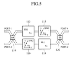
- Fig. 5 shows the second basic configuration of the optical non reciprocal circuit according to the present invention, in which the four terminal branching circuits 119 and 120 replaces the three terminal branching circuits 117 and 118 in the configuration of Fig. 3, so as to form an optical circulator in which either the even mode and the odd mode are combined/split, or the upper hald light and the lower half light interfere with each other.
- a light incoming from the port-1 is outputted to the port-2 while a light incoming from the port-2 is outputted to the port-3, and a light incoming from the port-3 is outputted to the port-4 while a light incoming from the port-4 is outputted to the port-1.
- the operation principle is similar to that described above with reference to Figs. 4A to 4D.
- Fig. 6 shows the first embodiment of the optical nonreciprocal circuit according to the present invention, which is based on the first basic configuration of Fig. 3.
- This optical nonreciprocal circuit of Fig. 6 comprises a magneto-optic waveguide 121 with two waveguide paths, Y-branching waveguides 122 and 123 provided on both sides of the magneto-optic waveguide 121, and half wave plates 124 and 125 inserted between the magneto-optic waveguide 121 and the Y-branching waveguides 122 and 123 respectively, on respective waveguide paths of the magneto-optic waveguide 121, where a magnetic field 126 is applied onto the magneto-optic waveguide 121.
- the magneto-optic waveguide 121 is made of the magneto-optic material YIG (Yttrium Iron Garnet) which is manufactured to form two waveguide paths. By applying the magnetic field 126, this magneto-optic waveguide 121 exhibits the nonreciprocal Faraday effect.
- the material of the magneto-optic waveguide 121 can be the substituted YIG.
- the material of the Y-branching waveguides 122 and 123 garnet, quartz, glass, etc. can be used.
- Fig. 7 shows the second embodiment of the optical nonreciprocal circuit according to the present invention, which is based on the first basic configuration of Fig. 3.
- This optical nonreciprocal circuit of Fig. 7 comprises an interferometer type magneto-optic waveguide 131 in which two waveguide paths functioning as the nonreciprocal rotators and Y-branching waveguides are integrally formed by the magneto-optic waveguide, and stress applying films 132 and 133 which are provided in the interferometer type magneto-optic waveguide 131 nearby the respective waveguide paths, where a magnetic field 134 is applied onto the interferometer type magneto-optic waveguide 131.
- the stress applying films 132 and 133 made of a-Si cause strain on the respective waveguide paths, so as to realize functions of the half wave plates.
- the interferometer type magneto-optic waveguide 131 incorporating the stress applying films 132 and 133 can be manufactured integrally, so that it is suitable for the optical integrated implementation.
- Fig. 8 shows the third embodiment of the optical nonreciprocal circuit according to the present invention, which is based on the second basic configuration of Fig. 5.
- This optical nonreciprocal circuit of Fig. 8 comprises a magneto-optic waveguide 181 with two waveguide paths, X-branching waveguides 182 and 183 provided on both sides of the magneto-optic waveguide 181, and half wave plates 184 and 185 inserted between the magneto-optic waveguide 181 and the X-branching waveguides 182 and 183 respectively, on respective waveguide paths of the magneto-optic waveguide 181, where a magnetic field 186 is applied onto the magneto-optic waveguide 181.
- the magneto-optic waveguide 181 is similar to the magneto-optic waveguide 121 of the first embodiment described above.
- the X-branching waveguides 182 and 183 combine/split the even mode and the odd mode.
- Fig. 9 shows the fourth embodiment of the optical nonreciprocal circuit according to the present invention, which is based on the second basic configuration of Fig. 5.
- This optical nonreciprocal circuit of Fig. 9 comprises an interferometer type magneto-optic waveguide 191 in which two waveguide paths functioning as the nonreciprocal rotators and X-brancing waveguides are integrally formed by the magneto-optic waveguide, and stress applying films 192 and 193 which are provided in the interferometer type magneto-optic waveguide 191 nearby the respective waveguide paths, where a magnetic field 194 is applied onto the interferometer type magneto-optic waveguide 191.
- the stress applying films 192 and 193 are similar to the stress applying films 132 and 133 of the second embodiment described above.
- the interferometer type magneto-optic waveguide 191 incorporating the stress applying films 192 and 193 can be manufactured integrally, so that it is suitable for the optical integrated implementation.
- Fig. 10 shows the fifth embodiment of the optical nonreciprocal circuit according to the present invention, which is based on the second basic configuration of Fig. 5.
- This optical nonreciprocal circuit of Fig. 10 comprises a magneto-optic waveguide 141 with two waveguide paths, four terminal branching waveguides 142 and 143 provided on both sides of the magneto-optic waveguide 141, and half wave plates 144 and 145 inserted between the magneto-optic waveguide 141 and the four terminal branching waveguides 142 and 143 respectively, on respective waveguide paths of the magneto-optic waveguide 141, where a magnetic field 146 is applied onto the magneto-optic waveguide 121.
- the magneto-optic waveguide 141 is similar to the magneto-optic waveguide 121 of the first embodiment described above.
- the four terminal branching waveguides 142 and 143 are formed by directional coupler waveguides which make the upper half light and the lower half light to interfere with each other.
- Fig. 11 shows the sixth embodiment of the optical nonreciprocal circuit according to the present invention, which is based on the second basic configuration of Fig. 5.
- This optical nonreciprocal circuit of Fig. 11 comprises an interferometer type magneto-optic waveguide 151 in which two waveguide paths functioning as the nonreciprocal rotators and directional couplers are integrally formed by the magneto-optic waveguide, and stress applying films 152 and 153 which are provided in the interferometer type magneto-optic waveguide 151 nearby the respective waveguide paths, where a magnetic field 154 is applied onto the interferometer type magneto-optic waveguide 151.
- the stress applying films 152 and 153 are similar to the stress applying films 132 and 133 of the second embodiment described above.
- the interferometer type magneto-optic waveguide 151 incorporating the stress applying films 152 and 153 can be manufactured integrally, so that it is suitable for the optical integrated implementation.
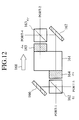
- Fig. 12 shows the seventh embodiment of the optical nonreciprocal circuit useful for understanding the present invention, which is based on the second basic configuration of Fig. 5.
- This optical nonreciprocal circuit of Fig. 12 comprises a magneto-optic crystal 161, half wave plates 164 and 165 provided on a lower half of the left side and an upper half of the right side of the magneto-optic crystal 161 respectively, beam splitters 162 and 163 provided next to the half wave plates 164 and 165 respectively, and mirrors 166 and 167 provided next to an upper half of the left side and a lower half of the right side of the magneto-optic crystal 161, where a magnetic field 168 is applied onto the magneto-optic crystal 161.
- This seventh embodiment has a structure in which light beams propagate through the space, rather than the waveguide structure of the previous embodiments.
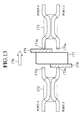
- Fig. 13 shows the eighth embodiment of the optical nonreciprocal circuit useful for understanding the present invention, which is based on the second basic configuration of Fig. 5.
- This optical nonreciprocal circuit of Fig. 13 comprises a magneto-optic crystal 171, optical fiber couplers 172 and 173 provided on both sides of the magneto-optic crystal 171, and half wave plates 174 and 175 inserted between the magneto-optic crystal 171 and the optical fiber couplers 172 and 173 respectively and provided on a lower half of the left side and an upper half of the right side of the magneto-optic crystal 171 respectively, where a magnetic field 176 is applied onto the magneto-optic crystal 171.
- the branching circuits and the optical paths of Fig. 5 are formed by the known optical fiber couplers 172 and 173, each of which is formed by fusion connecting two optical fibers. Tip edges 172a and 173a of the optical fibers facing toward the magneto-optic crystal 171 has enlarged cores, so that the spread of the outgoing light beams can be suppressed. Because of the use of the optical fibers, the optical nonreciprocal circuit of Fig. 13 is easier to manufacture. For the optical fibers, the usual optical fibers can be used, but it is also possible to use the polarization maintaining fibers.
- Fig. 14 shows the ninth embodiment of the optical nonreciprocal circuit useful for understanding the present invention, which is based on the second basic configuration of Fig. 5.
- a phase adjustment unit 177 is additionally provided in at least one of the optical fibers constituting the optical fiber couplers 172 and 173 in the configuration of Fig. 13.
- the phase adjustment unit 177 makes the adjustment of the phase by means of the change of the refractive index caused by applying ultraviolet ray or heat to a part of the optical fiber, for example.
- the rest of this configuration of Fig. 14 and its operation in this ninth embodiment is the same as the eighth embodiment described above.
- phase adjustment unit of this ninth embodiment can be used in conjunction with any of the first to eighth embodiments described above.
- optical nonreciprocal circuit of any of the first to ninth embodiments described above requires a use of optical branching circuits and utilizes the interferences, so that some phase adjustment is indispensable in practice.
- FIG. 15 to Fig. 20 further embodiments of the optical nonreciprocal circuit useful for understanding the present invention which are directed to an inexpensive optical nonreciprocal circuit, which does not require a use of expensive birefringent crystals, optical branching circuits, and a phase adjustment, will be described in detail.
- Fig. 15 shows the tenth embodiment of the optical nonreciprocal circuit useful for understanding the present invention.
- This optical nonreciprocal circuit of Fig. 15 comprises single mode optical fibers 221 and 222, lenses 223 and 224 provided between the single mode optical fibers 221 and 222, a Faraday rotator 225 provided on an upper half of a space between the lenses 223 and 224, a Faraday rotator 226 provided on a lower hald of a space between the leses 223 and 224, a half wave plate 227 provided on the lense 224 side of the Faraday rotator 225, and a half wave plate 228 provided on the lense 223 side of the Faraday rotator 226, where a magnetic field 229 is applied onto the Faraday rotators 225 and 226.
- a light incoming from the single mode fiber 221 is turned into a parallel beam 230 by the lens 223, and an upper half of the parallel beam 230 passes through the Faraday rotator 225 and the half wave plate 227 while a lower half of the parallel beam 230 passes through the half wave plate 228 and the Faraday rotator 226.
- the upper and lower halves of the parallel beam 230 are then collimated by the lens 224 and coupled into the single mode optical fiber 222.
- a light incoming from the single mode optical fiber 222 is turned into a parallel beam 230 by the lens 224, and an upper half of the parallel beam 230 passes through the half wave plate 227 and the Faraday rotator 225 while a lower half of the parallel beam 230 passes through the Faraday rotator 226 and the half wave plate 228.
- the upper half and the lower half of the parallel beam 230 are then collimated by the lens 223 and coupled into the single mode optical fiber 221.
- a direction of a light propagaing toward the right direction will be taken as a z-axis
- x-axis and y-axis are suitably set within a plane perpendicular to the z-axis
- a clockwise rotation will be taken as a positive rotation.
- the Faraday rotation angles of the Faraday rotators 225 and 226 will be denoted as ⁇ f1 and ⁇ f2 , respectively
- the slow axis angle of the half wave plates 227 and 228 with respect to the x-axis will be denoted as ⁇ s1 and ⁇ s2 , respectively.
- Fig. 16A and Fig. 16B show electric field distributions at A-A' plane and D-D' plane located at the tip ends of the single mode optical fibers 221 and 222 as indicated in Fig. 15, and polarization states of the parallel beam 230 at B-B' plane and C-C' plane as indicated in Fig. 15, for a light incoming from the single mode optical fiber 221 and a light incoming from the single mode optical fiber 222, respectively.
- the electric field distribution of a light incoming from the single mode optical fiber 221 is symmetric in the even guided mode at A-A' plane, and after passing through the lens 223, the upper half and the lower half of the parallel beam 230 have the same polarization at B-B' plane.
- the upper half and the lower half of the parallel beam 230 still have the same polarization at C-C' plane.
- the electric field distribution of the light collimated by the lens 224 is also symmetric in the even guided mode at D-D' plane, so that the upper half and the lower half of the light are coupled into the single mode optical fiber 222.
- the electric field distribution of a light incoming from the single mode optical fiber 222 is symmetric in the even guided mode at D-D' plane, and after passing through the lens 224, the upper half and the lower half of the parallel beam 230 have the same polarization at C-C' plane.
- the upper half and the lower half of the parallel beam 230 have the opposite polarizations at B-B' plane.
- the electric field distribution of the light collimated by the lens 223 is antisymmetric in the odd non-guided mode at A-A' plane, so that the upper half and the lower half of the light are not coupled into the single mode optical fiber 221 and dissipated.
- the polarization independent optical isolator is realized by the configuration of Fig. 15 according to this tenth embodiment.
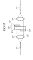
- Fig. 17 shows the eleventh embodiment of the optical nonreciprocal circuit useful for understanding the present invention.
- Fig. 18 shows the twelfth embodiment of the optical nonreciprocal circuit useful for understanding the present invention.
- Fig. 19 shows the thirteenth embodiment of the optical nonreciprocal circuit useful for understanding the present invention.
- the functions of a pair of the Faraday rotator 225 and the half wave plate 227 and a pair of the Faraday rotator 226 and the half wave plate 228 in the configuration of Fig. 15 are provided in two stages, by a pair of a Faraday rotator 225A and a half wave plate 227A and a pair of a Faraday rotator 226A and a half wave plate 228A on the first stage, and a pair of a Faraday rotator 225B and a half wave plate 227B and a pair of a Faraday 226B and a half wave plate 228B on the second stage.
- a direction in which the Faraday rotator-half wave plate pairs on the first stage are arranged is set perpendicular to a direction in which the Faraday rotator-half wave plate pairs on the second state are arranged, so that the Faraday rotator-half wave plate pairs on the first stage divide the light into an upper half and a lower half (along x-axis) while the Faraday rotator-half wave plate pairs on the second stage divide the light into a left half and a right half (along y-axis).
- the backward light which was not completely turned into the odd non-guided mode at the first stage can be completely turned into the odd non-guided mode at the second stage, so as to improve the isolation of the light. Since the first stage and the second stage are arranged perpendicular to each other, the backward light which was turned into the odd non-guided mode at the first stage would not be turned into the even guided mode at the second stage.
- Fig. 20 shows the fourteenth embodiment of the optical nonreciprocal circuit useful for understanding the present invention.
- a single Faraday rotator 231A replaces two Faraday rotators 225A and 226A of the first stage in the configuration of Fig. 15, and a single Faraday rotator 231B replaces two Faraday rotators 225B and 226B of the second stage in the configuration of Fig. 15.
- the rest of this configuration of Fig. 20 and its operation in this fourteenth embodiment are the same as the tenth embodiment described above.
- the split parts of the light propagating forward are combined with the identical polarization so that the light is outputted while maintaining its original power, whereas the split parts of the light propagating backward are combined with the opposite polarizations so that the light is not outputted as its power is dissipated. Consequently, it is possible to realize an inexpensive optical nonreciprocal circuit which is suitable for the integrated implementation, without requiring a use of polarization beam splitters which are expensive and not suitable for the integrated implementation.
- the optical nonreciprocal circuit of the tenth to fourteenth embodiments described above at a time of coupling the light between two optical waveguides using a lens, by sequentially applying the nonreciprocal rotation and the reciprocal rotation to a half of the light while sequentially applying the reciprocal rotation and the nonreciprocal rotation to another half of the light, the halves of the light propagating forward are combined with the identical polarization into the even guided mode and coupled so that the light is outputted while maintaining its original power, whereas the halves of the light propagating backward are combined with the opposite polarizations into the odd non-guided mode and not coupled so that the light is not outputted as its power is dissipated. Consequently, it is possible to realize an inexpensive optical nonreciprocal circuit which does not require a use of expensive birefringent crystals, optical branching circuits and a phase adjustment.
- a polarization independent optical nonreciprocal circuit which is capable of providing a large degree of freedom in its configuration and of eliminating the polarization dependent loss due to the branching circuits such as directional couplers, even in a configuration which does not require a use of polarization beam splitters.
- optical nonreciprocal circuit functions as an optical switch or an optical variable attenuator by changing a direction and an amount of currents supplied to the electromagnet.
- the optical nonreciprocal circuit of any of the first to fourteenth embodiments described above may be modified to function as an optical switch or an optical variable attenuator by utilizing such an electromagnet.
Landscapes
- Physics & Mathematics (AREA)
- Nonlinear Science (AREA)
- Engineering & Computer Science (AREA)
- Power Engineering (AREA)
- General Physics & Mathematics (AREA)
- Optics & Photonics (AREA)
- Optical Integrated Circuits (AREA)
Claims (10)
- Un circuit optique non réciproque pour diviser/combiner des lumières, comprenant :dans lesquels f1, f2, s1, et s2 satisfont à :un premier chemin optique (111) et un second chemin optique (112) par l'intermédiaire desquels des première et seconde lumières divisées se propagent ;un premier circuit de division/combinaison (117, 119, 172), prévu sur une extrémité des premier et second chemins optiques (111, 112), pour diviser de la lumière reçue en première et seconde lumières divisées dans une première direction le long des premier et second chemins optiques (111, 112), et pour combiner la lumière se propageant le long des premier et second chemins optiques (111, 112) dans une deuxième direction opposée à la première direction ;un premier circuit de rotation de polarisation (113, 115) prévu sur le premier chemin optique (111), comprenant un premier rotateur non réciproque (113) ayant un angle de rotation de Faraday f1, et un premier rotateur réciproque (115) formé par une plaque demi-onde ayant un angle d'axe lent s1 par rapport à un axe x dans des coordonnées x-y établies dans un plan perpendiculaire à une direction de propagation de la lumière, qui sont prévus par rapport à la première lumière divisée ; etun second circuit de rotation de polarisation (114, 116) prévu sur le second chemin optique (112), comprenant un second rotateur réciproque (116) formé par une plaque demi-onde ayant un angle d'axe lent s2 par rapport à l'axe x, et un second rotateur non réciproque (114) ayant un angle de rotation de Faraday f2, qui sont prévus par rapport à la seconde lumière divisée ;
caractérisé en ce que :la première lumière divisée et la seconde lumière divisée se propageant dans la première direction ont une polarisation identique et sont combinées pour former un mode pair, tandis que la première lumière divisée et la seconde lumière divisée se propageant dans la seconde direction ont des polarisations opposées et sont combinées pour former un mode impair ; etles premier et second rotateurs non réciproques (113, 114) comprennent chacun un guide d'ondes magnéto-optiques (121, 131, 151, 181, 191) constituant au moins une partie des premier et second chemins optiques (111, 112) auxquels un champ magnétique (126, 134, 146, 154, 186, 194) est appliqué dans une direction parallèle à la direction de propagation du guide d'ondes. - Le circuit optique non réciproque selon la revendication 1, dans lequel les premier et second rotateurs réciproques (115, 116) sont réalisés par des films d'application de contrainte (132, 133, 192, 193), prévus dans des voisinages des premier et second chemins optiques (111, 112), qui provoquent une contrainte sur les premier et second chemins optiques (111, 112).
- Le circuit optique non réciproque selon la revendication 2, comprenant en outre :dans lequel le guide d'ondes magnéto-optiques (131, 151, 191), les films d'application de contrainte (132, 133, 152, 153, 192, 193), et les premier et second circuits de division/combinaison (117, 118, 119, 120) sont formés intégralement comme un circuit de guide d'ondes magnéto-optiques (131, 151, 191) du type interféromètre.un second circuit de division/combinaison (118, 120), prévu sur une autre extrémité des premier et second chemins optiques (111, 112), pour diviser de la lumière se propageant dans la seconde direction en première et seconde lumières divisées et pour sortir les première et seconde lumières divisées vers les premier et second chemins optiques (111, 112), et combiner de la lumière se propageant dans la première direction le long des premier et second chemins optiques (111, 112) ;
- Le circuit optique non réciproque selon la revendication 1, comprenant de plus :un second circuit de division/combinaison (118, 120, 173), prévu sur une autre extrémité des premier et second chemins optiques (111, 112), pour.diviser de la lumière se propageant dans la seconde direction en première et seconde lumières divisées et pour sortir les première et seconde lumières divisées vers les premier et second chemins optiques (111, 112), et combiner de la lumière se propageant dans la première direction le long des premier et second chemins optiques (111, 112).
- Le circuit optique non réciproque selon la revendication 4, dans lequel chacun des premier et second circuits de division/combinaison (117, 118) est un circuit à ramification en Y, de sorte que le circuit optique non réciproque constitue un isolant optique.
- Le circuit optique non réciproque selon la revendication 4, dans lequel chacun des premier et second circuits de division/combinaison (119, 120) est un circuit à ramification en X, de sorte que le circuit optique non réciproque constitue un circulateur optique.
- Le circuit optique non réciproque selon la revendication 4, dans lequel chacun des premier et second circuits de division/combinaison (172, 173) est un coupleur de fibre optique.
- Le circuit optique non réciproque selon la revendication 1, dans lequel au moins un des premier et second chemins optiques (111, 112) comprend un circuit d'ajustement de phase (177) pour ajuster une -phase de la lumière se propageant à travers ledit au moins un chemin des premier et second chemins optiques (111, 112).
- Le circuit optique non réciproque selon la revendication 1, dans lequel f1, f2, s1, et s2 satisfont également à :
- Un circuit optique non réciproque pour diviser/combiner des lumières, comprenant :dans lesquels f1, f2, s1, et s2 satisfont à :un premier chemin optique (111) et un second chemin optique (112) par lesquels des première et seconde lumières divisées se propagent ;un premier coupleur directionnel (172), prévu sur une extrémité des premier et second chemins optiques (111, 112), pour diviser de la lumière reçue en première et seconde lumières divisées dans une première direction le long des premier et second chemins optiques (111, 112), et pour combiner la lumière se propageant le long des premier et second chemins optiques (111, 112) dans une seconde direction opposée à la première direction ;un second coupleur directionnel (173), prévu sur une autre extrémité des premier et second chemins optiques (111, 112), pour diviser de la lumière se propageant dans la seconde direction en première et seconde lumières divisées et pour sortir les première et seconde lumières divisées vers les premier et second chemins optiques (111, 112), et combiner de la lumière se propageant dans la première direction le long des premier et second chemins optiques (111, 112) ;un premier circuit de rotation de polarisation (113, 115) prévu sur le premier chemin optique (111), incluant un premier rotateur non réciproque (113) ayant un angle de rotation de Faraday f1, et un premier rotateur réciproque (115) formé par une plaque demi-onde ayant un angle d'axe lent s1 par rapport à un axe x dans des coordonnées x-y établies dans un plan perpendiculaire à une direction de propagation de la lumière, qui sont prévus par rapport à la première lumière divisée ; etun second circuit de rotation de polarisation (114, 116) prévu sur le second chemin optique (112), incluant un second rotateur réciproque (116) formé par une plaque demi-onde ayant un angle d'axe lent s2 par rapport à l'axe x et un second rotateur non réciproque (114) ayant un angle de rotation de Faraday f2, qui sont prévus par rapport à la seconde lumière divisée ;
CARACTERISE EN CE QUE
f1, f2, s1, et s2 ne satisfont pas à s1 = 3π / 8, s2 = 5π / 8, et f1 = f2 = π / 4 simultanément ; et
les premier et second rotateurs non réciproques (113, 114) incluent chacun un guide d'ondes magnéto-optiques (121, 131, 151, 181, 191) constituant au moins une partie des premier et second chemins optiques (111, 112), auxquels un champ magnétique (126, 134, 146, 154, 186, 194) est appliqué dans une direction parallèle à la direction de propagation du guide d'ondes.
Applications Claiming Priority (6)
| Application Number | Priority Date | Filing Date | Title |
|---|---|---|---|
| JP41702/96 | 1996-02-28 | ||
| JP4170296 | 1996-02-28 | ||
| JP4170296 | 1996-02-28 | ||
| JP15722896 | 1996-06-18 | ||
| JP157228/96 | 1996-06-18 | ||
| JP15722896 | 1996-06-18 |
Publications (2)
| Publication Number | Publication Date |
|---|---|
| EP0793130A1 EP0793130A1 (fr) | 1997-09-03 |
| EP0793130B1 true EP0793130B1 (fr) | 2002-08-28 |
Family
ID=26381350
Family Applications (1)
| Application Number | Title | Priority Date | Filing Date |
|---|---|---|---|
| EP97103351A Expired - Lifetime EP0793130B1 (fr) | 1996-02-28 | 1997-02-28 | Dispositif optique non réciproque insensible à la polarisation |
Country Status (3)
| Country | Link |
|---|---|
| US (1) | US5905823A (fr) |
| EP (1) | EP0793130B1 (fr) |
| DE (1) | DE69714889T2 (fr) |
Families Citing this family (19)
| Publication number | Priority date | Publication date | Assignee | Title |
|---|---|---|---|---|
| KR100216980B1 (ko) * | 1996-12-05 | 1999-09-01 | 윤덕용 | 광주파수 변환을 이용한 비가역적 광소자 |
| KR100275653B1 (ko) * | 1998-03-04 | 2001-01-15 | 박호군 | 편광의존형 방향성 고립기 및 이를 이용한 고리형 공진기레이저 |
| CA2273641A1 (fr) * | 1999-06-04 | 2000-12-04 | Robert I. Macdonald | Interferometre sagnac a commutation de polarisation et applications |
| TW440712B (en) * | 2000-06-07 | 2001-06-16 | Ind Tech Res Inst | Optical circulator |
| US7043100B2 (en) * | 2001-01-25 | 2006-05-09 | E. I. Du Pont De Nemours And Company | Polarization independent waveguide optical isolator and circulator |
| JP2002268013A (ja) * | 2001-03-09 | 2002-09-18 | Furukawa Electric Co Ltd:The | 光サーキュレータ |
| US6748126B2 (en) | 2001-12-31 | 2004-06-08 | 3M Innovative Properties Company | System for polarization mode dispersion compensation |
| US7263247B1 (en) | 2002-02-11 | 2007-08-28 | Gemfire Corporation | Integrated optical isolator array |
| JP4927548B2 (ja) * | 2004-08-04 | 2012-05-09 | 古河電気工業株式会社 | 光回路装置 |
| US7260282B2 (en) * | 2005-03-30 | 2007-08-21 | Intel Corporation | Integratable optical waveguide isolator |
| US7260281B2 (en) * | 2005-03-30 | 2007-08-21 | Intel Corporation | Integratable optical isolator in a Mach-Zehnder interferometer configuration |
| WO2007108544A1 (fr) * | 2006-03-20 | 2007-09-27 | Tokyo Institute Of Technology | isolateur optique indépendant de LA polarisation de l'ONDE |
| US7555177B1 (en) * | 2006-04-12 | 2009-06-30 | Iowa State University Research Foundation, Inc. | All fiber magneto-optic on-off switch for networking applications |
| US7916982B1 (en) | 2006-04-12 | 2011-03-29 | Iowa State University Research Foundation | All fiber magneto-optic on-off switch for networking applications |
| TWI372270B (en) * | 2009-05-04 | 2012-09-11 | Ind Tech Res Inst | Optical switch and communication system of optical signal |
| FR3002654A1 (fr) | 2013-02-26 | 2014-08-29 | St Microelectronics Sa | Modulateur optique avec correction de polarisation automatique |
| US10254477B2 (en) * | 2015-12-09 | 2019-04-09 | Finisar Corporation | Polarization independent multiplexer / demultiplexer |
| US10670891B2 (en) | 2016-12-30 | 2020-06-02 | Samsung Electronics Co., Ltd. | Nonreciprocal optical transmission device and optical apparatus including the same |
| JP7208098B2 (ja) | 2019-04-25 | 2023-01-18 | 京セラ株式会社 | 光アイソレータ及び光源装置 |
Family Cites Families (8)
| Publication number | Priority date | Publication date | Assignee | Title |
|---|---|---|---|---|
| US4239329A (en) * | 1978-08-04 | 1980-12-16 | Nippon Telegraph And Telephone Public Corporation | Optical nonreciprocal device |
| US5033830A (en) * | 1989-10-04 | 1991-07-23 | At&T Bell Laboratories | Polarization independent optical isolator |
| US4978189A (en) * | 1989-11-14 | 1990-12-18 | At&T Bell Laboratories | Hybrid optical isolator, circulator or switch, and systems utilizing same |
| JPH03288104A (ja) * | 1990-04-04 | 1991-12-18 | Agency Of Ind Science & Technol | 一方向性モード変換器およびそれを用いた光アイソレータ |
| DE69121176T2 (de) * | 1990-12-17 | 1997-01-09 | Nippon Telegraph & Telephone | Optischer Zirkulator |
| EP0634025A4 (fr) * | 1992-04-03 | 1995-05-17 | Australian & Overseas Telecom | Ameliorations concernant le dephasage optique. |
| US5471340A (en) * | 1994-01-07 | 1995-11-28 | Jds Fitel Inc. | Reflective optical non-reciprocal devices |
| JPH0850261A (ja) * | 1994-08-05 | 1996-02-20 | Nippon Telegr & Teleph Corp <Ntt> | 光サーキュレータ |
-
1997
- 1997-02-28 EP EP97103351A patent/EP0793130B1/fr not_active Expired - Lifetime
- 1997-02-28 DE DE69714889T patent/DE69714889T2/de not_active Expired - Fee Related
- 1997-02-28 US US08/810,321 patent/US5905823A/en not_active Expired - Fee Related
Also Published As
| Publication number | Publication date |
|---|---|
| DE69714889D1 (de) | 2002-10-02 |
| US5905823A (en) | 1999-05-18 |
| DE69714889T2 (de) | 2003-04-10 |
| EP0793130A1 (fr) | 1997-09-03 |
Similar Documents
| Publication | Publication Date | Title |
|---|---|---|
| EP0793130B1 (fr) | Dispositif optique non réciproque insensible à la polarisation | |
| CA2141109C (fr) | Isolateur optique insensible a la polarisation | |
| Sugimoto et al. | Waveguide polarization-independent optical circulator | |
| EP0491607A2 (fr) | Circulateur optique | |
| US20020131171A1 (en) | Optical fiber polarization independent non-reciprocal phase shifter | |
| US6757451B2 (en) | Optical circulator | |
| JPH09189885A (ja) | 光学装置 | |
| US6002512A (en) | Optical circulator using latchable garnet | |
| JPH05196890A (ja) | 光アイソレータ | |
| US6112000A (en) | Reflective array multiplexer with polarization compensation | |
| US20020044710A1 (en) | Optical fiber non-reciprocal phase shifter | |
| EP1389739A1 (fr) | Circulateur optique utilisant circuits à onde lumineuse planaire | |
| US11886058B2 (en) | Optical isolator | |
| US6278547B1 (en) | Polarization insensitive faraday attenuator | |
| JPH07281128A (ja) | 光アイソレータ | |
| US6246807B1 (en) | Optical circulator | |
| JPH1068910A (ja) | 光非相反回路 | |
| JP2758457B2 (ja) | 導波路型光サーキュレータ | |
| JP2989982B2 (ja) | ファイバ型光アイソレータ | |
| JP3540826B2 (ja) | ファイバ型光アイソレータ | |
| JPH04102821A (ja) | 偏光無依存型光アイソレータ | |
| JPH11119158A (ja) | 光サーキュレータアレイ | |
| JP2004177639A (ja) | 反射型可変磁気光学デバイス | |
| JP3457710B2 (ja) | 光ファイバ部品 | |
| JPH08171075A (ja) | 光スイッチ |
Legal Events
| Date | Code | Title | Description |
|---|---|---|---|
| PUAI | Public reference made under article 153(3) epc to a published international application that has entered the european phase |
Free format text: ORIGINAL CODE: 0009012 |
|
| 17P | Request for examination filed |
Effective date: 19970228 |
|
| AK | Designated contracting states |
Kind code of ref document: A1 Designated state(s): DE GB IT |
|
| 17Q | First examination report despatched |
Effective date: 19990615 |
|
| GRAG | Despatch of communication of intention to grant |
Free format text: ORIGINAL CODE: EPIDOS AGRA |
|
| GRAG | Despatch of communication of intention to grant |
Free format text: ORIGINAL CODE: EPIDOS AGRA |
|
| GRAH | Despatch of communication of intention to grant a patent |
Free format text: ORIGINAL CODE: EPIDOS IGRA |
|
| GRAH | Despatch of communication of intention to grant a patent |
Free format text: ORIGINAL CODE: EPIDOS IGRA |
|
| GRAA | (expected) grant |
Free format text: ORIGINAL CODE: 0009210 |
|
| AK | Designated contracting states |
Kind code of ref document: B1 Designated state(s): DE GB IT |
|
| REG | Reference to a national code |
Ref country code: GB Ref legal event code: FG4D |
|
| REF | Corresponds to: |
Ref document number: 69714889 Country of ref document: DE Date of ref document: 20021002 |
|
| PLBE | No opposition filed within time limit |
Free format text: ORIGINAL CODE: 0009261 |
|
| STAA | Information on the status of an ep patent application or granted ep patent |
Free format text: STATUS: NO OPPOSITION FILED WITHIN TIME LIMIT |
|
| 26N | No opposition filed |
Effective date: 20030530 |
|
| PGFP | Annual fee paid to national office [announced via postgrant information from national office to epo] |
Ref country code: DE Payment date: 20090225 Year of fee payment: 13 |
|
| PGFP | Annual fee paid to national office [announced via postgrant information from national office to epo] |
Ref country code: IT Payment date: 20100128 Year of fee payment: 14 |
|
| PGFP | Annual fee paid to national office [announced via postgrant information from national office to epo] |
Ref country code: GB Payment date: 20100118 Year of fee payment: 14 |
|
| PG25 | Lapsed in a contracting state [announced via postgrant information from national office to epo] |
Ref country code: DE Free format text: LAPSE BECAUSE OF NON-PAYMENT OF DUE FEES Effective date: 20100901 |
|
| GBPC | Gb: european patent ceased through non-payment of renewal fee |
Effective date: 20110228 |
|
| PG25 | Lapsed in a contracting state [announced via postgrant information from national office to epo] |
Ref country code: IT Free format text: LAPSE BECAUSE OF NON-PAYMENT OF DUE FEES Effective date: 20110228 |
|
| PG25 | Lapsed in a contracting state [announced via postgrant information from national office to epo] |
Ref country code: GB Free format text: LAPSE BECAUSE OF NON-PAYMENT OF DUE FEES Effective date: 20110228 |