EP0791803A2 - Cantilever unit and atomic force microscope, magnetic force microscope, reproducing apparatus and information processing apparatus using the cantilever unit - Google Patents
Cantilever unit and atomic force microscope, magnetic force microscope, reproducing apparatus and information processing apparatus using the cantilever unit Download PDFInfo
- Publication number
- EP0791803A2 EP0791803A2 EP97200263A EP97200263A EP0791803A2 EP 0791803 A2 EP0791803 A2 EP 0791803A2 EP 97200263 A EP97200263 A EP 97200263A EP 97200263 A EP97200263 A EP 97200263A EP 0791803 A2 EP0791803 A2 EP 0791803A2
- Authority
- EP
- European Patent Office
- Prior art keywords
- cantilever
- unit
- probe
- force microscope
- detecting means
- Prior art date
- Legal status (The legal status is an assumption and is not a legal conclusion. Google has not performed a legal analysis and makes no representation as to the accuracy of the status listed.)
- Granted
Links
Images


Classifications
-
- G—PHYSICS
- G01—MEASURING; TESTING
- G01B—MEASURING LENGTH, THICKNESS OR SIMILAR LINEAR DIMENSIONS; MEASURING ANGLES; MEASURING AREAS; MEASURING IRREGULARITIES OF SURFACES OR CONTOURS
- G01B9/00—Measuring instruments characterised by the use of optical techniques
- G01B9/02—Interferometers
- G01B9/02049—Interferometers characterised by particular mechanical design details
- G01B9/02051—Integrated design, e.g. on-chip or monolithic
-
- G—PHYSICS
- G01—MEASURING; TESTING
- G01B—MEASURING LENGTH, THICKNESS OR SIMILAR LINEAR DIMENSIONS; MEASURING ANGLES; MEASURING AREAS; MEASURING IRREGULARITIES OF SURFACES OR CONTOURS
- G01B9/00—Measuring instruments characterised by the use of optical techniques
- G01B9/02—Interferometers
- G01B9/02015—Interferometers characterised by the beam path configuration
- G01B9/02022—Interferometers characterised by the beam path configuration contacting one object by grazing incidence
-
- G—PHYSICS
- G01—MEASURING; TESTING
- G01B—MEASURING LENGTH, THICKNESS OR SIMILAR LINEAR DIMENSIONS; MEASURING ANGLES; MEASURING AREAS; MEASURING IRREGULARITIES OF SURFACES OR CONTOURS
- G01B9/00—Measuring instruments characterised by the use of optical techniques
- G01B9/02—Interferometers
- G01B9/02015—Interferometers characterised by the beam path configuration
- G01B9/02023—Indirect probing of object, e.g. via influence on cavity or fibre
-
- G—PHYSICS
- G01—MEASURING; TESTING
- G01P—MEASURING LINEAR OR ANGULAR SPEED, ACCELERATION, DECELERATION, OR SHOCK; INDICATING PRESENCE, ABSENCE, OR DIRECTION, OF MOVEMENT
- G01P15/00—Measuring acceleration; Measuring deceleration; Measuring shock, i.e. sudden change of acceleration
- G01P15/02—Measuring acceleration; Measuring deceleration; Measuring shock, i.e. sudden change of acceleration by making use of inertia forces using solid seismic masses
- G01P15/08—Measuring acceleration; Measuring deceleration; Measuring shock, i.e. sudden change of acceleration by making use of inertia forces using solid seismic masses with conversion into electric or magnetic values
- G01P15/0894—Measuring acceleration; Measuring deceleration; Measuring shock, i.e. sudden change of acceleration by making use of inertia forces using solid seismic masses with conversion into electric or magnetic values by non-contact electron transfer, i.e. electron tunneling
-
- G—PHYSICS
- G01—MEASURING; TESTING
- G01Q—SCANNING-PROBE TECHNIQUES OR APPARATUS; APPLICATIONS OF SCANNING-PROBE TECHNIQUES, e.g. SCANNING PROBE MICROSCOPY [SPM]
- G01Q20/00—Monitoring the movement or position of the probe
- G01Q20/02—Monitoring the movement or position of the probe by optical means
-
- G—PHYSICS
- G01—MEASURING; TESTING
- G01Q—SCANNING-PROBE TECHNIQUES OR APPARATUS; APPLICATIONS OF SCANNING-PROBE TECHNIQUES, e.g. SCANNING PROBE MICROSCOPY [SPM]
- G01Q60/00—Particular types of SPM [Scanning Probe Microscopy] or microscopes; Essential components thereof
- G01Q60/02—Multiple-type SPM, i.e. involving more than one SPM techniques
- G01Q60/08—MFM [Magnetic Force Microscopy] combined with AFM [Atomic Force Microscopy
-
- G—PHYSICS
- G01—MEASURING; TESTING
- G01Q—SCANNING-PROBE TECHNIQUES OR APPARATUS; APPLICATIONS OF SCANNING-PROBE TECHNIQUES, e.g. SCANNING PROBE MICROSCOPY [SPM]
- G01Q60/00—Particular types of SPM [Scanning Probe Microscopy] or microscopes; Essential components thereof
- G01Q60/24—AFM [Atomic Force Microscopy] or apparatus therefor, e.g. AFM probes
- G01Q60/38—Probes, their manufacture, or their related instrumentation, e.g. holders
-
- G—PHYSICS
- G01—MEASURING; TESTING
- G01Q—SCANNING-PROBE TECHNIQUES OR APPARATUS; APPLICATIONS OF SCANNING-PROBE TECHNIQUES, e.g. SCANNING PROBE MICROSCOPY [SPM]
- G01Q60/00—Particular types of SPM [Scanning Probe Microscopy] or microscopes; Essential components thereof
- G01Q60/50—MFM [Magnetic Force Microscopy] or apparatus therefor, e.g. MFM probes
- G01Q60/54—Probes, their manufacture, or their related instrumentation, e.g. holders
- G01Q60/56—Probes with magnetic coating
-
- G—PHYSICS
- G01—MEASURING; TESTING
- G01R—MEASURING ELECTRIC VARIABLES; MEASURING MAGNETIC VARIABLES
- G01R33/00—Arrangements or instruments for measuring magnetic variables
- G01R33/02—Measuring direction or magnitude of magnetic fields or magnetic flux
- G01R33/038—Measuring direction or magnitude of magnetic fields or magnetic flux using permanent magnets, e.g. balances, torsion devices
- G01R33/0385—Measuring direction or magnitude of magnetic fields or magnetic flux using permanent magnets, e.g. balances, torsion devices in relation with magnetic force measurements
-
- G—PHYSICS
- G11—INFORMATION STORAGE
- G11B—INFORMATION STORAGE BASED ON RELATIVE MOVEMENT BETWEEN RECORD CARRIER AND TRANSDUCER
- G11B9/00—Recording or reproducing using a method not covered by one of the main groups G11B3/00 - G11B7/00; Record carriers therefor
- G11B9/12—Recording or reproducing using a method not covered by one of the main groups G11B3/00 - G11B7/00; Record carriers therefor using near-field interactions; Record carriers therefor
- G11B9/14—Recording or reproducing using a method not covered by one of the main groups G11B3/00 - G11B7/00; Record carriers therefor using near-field interactions; Record carriers therefor using microscopic probe means, i.e. recording or reproducing by means directly associated with the tip of a microscopic electrical probe as used in Scanning Tunneling Microscopy [STM] or Atomic Force Microscopy [AFM] for inducing physical or electrical perturbations in a recording medium; Record carriers or media specially adapted for such transducing of information
- G11B9/1409—Heads
-
- G—PHYSICS
- G11—INFORMATION STORAGE
- G11B—INFORMATION STORAGE BASED ON RELATIVE MOVEMENT BETWEEN RECORD CARRIER AND TRANSDUCER
- G11B9/00—Recording or reproducing using a method not covered by one of the main groups G11B3/00 - G11B7/00; Record carriers therefor
- G11B9/12—Recording or reproducing using a method not covered by one of the main groups G11B3/00 - G11B7/00; Record carriers therefor using near-field interactions; Record carriers therefor
- G11B9/14—Recording or reproducing using a method not covered by one of the main groups G11B3/00 - G11B7/00; Record carriers therefor using near-field interactions; Record carriers therefor using microscopic probe means, i.e. recording or reproducing by means directly associated with the tip of a microscopic electrical probe as used in Scanning Tunneling Microscopy [STM] or Atomic Force Microscopy [AFM] for inducing physical or electrical perturbations in a recording medium; Record carriers or media specially adapted for such transducing of information
- G11B9/1418—Disposition or mounting of heads or record carriers
-
- G—PHYSICS
- G01—MEASURING; TESTING
- G01B—MEASURING LENGTH, THICKNESS OR SIMILAR LINEAR DIMENSIONS; MEASURING ANGLES; MEASURING AREAS; MEASURING IRREGULARITIES OF SURFACES OR CONTOURS
- G01B2290/00—Aspects of interferometers not specifically covered by any group under G01B9/02
- G01B2290/30—Grating as beam-splitter
-
- G—PHYSICS
- G01—MEASURING; TESTING
- G01Q—SCANNING-PROBE TECHNIQUES OR APPARATUS; APPLICATIONS OF SCANNING-PROBE TECHNIQUES, e.g. SCANNING PROBE MICROSCOPY [SPM]
- G01Q80/00—Applications, other than SPM, of scanning-probe techniques
-
- Y—GENERAL TAGGING OF NEW TECHNOLOGICAL DEVELOPMENTS; GENERAL TAGGING OF CROSS-SECTIONAL TECHNOLOGIES SPANNING OVER SEVERAL SECTIONS OF THE IPC; TECHNICAL SUBJECTS COVERED BY FORMER USPC CROSS-REFERENCE ART COLLECTIONS [XRACs] AND DIGESTS
- Y10—TECHNICAL SUBJECTS COVERED BY FORMER USPC
- Y10S—TECHNICAL SUBJECTS COVERED BY FORMER USPC CROSS-REFERENCE ART COLLECTIONS [XRACs] AND DIGESTS
- Y10S977/00—Nanotechnology
- Y10S977/84—Manufacture, treatment, or detection of nanostructure
- Y10S977/849—Manufacture, treatment, or detection of nanostructure with scanning probe
- Y10S977/86—Scanning probe structure
- Y10S977/868—Scanning probe structure with optical means
-
- Y—GENERAL TAGGING OF NEW TECHNOLOGICAL DEVELOPMENTS; GENERAL TAGGING OF CROSS-SECTIONAL TECHNOLOGIES SPANNING OVER SEVERAL SECTIONS OF THE IPC; TECHNICAL SUBJECTS COVERED BY FORMER USPC CROSS-REFERENCE ART COLLECTIONS [XRACs] AND DIGESTS
- Y10—TECHNICAL SUBJECTS COVERED BY FORMER USPC
- Y10S—TECHNICAL SUBJECTS COVERED BY FORMER USPC CROSS-REFERENCE ART COLLECTIONS [XRACs] AND DIGESTS
- Y10S977/00—Nanotechnology
- Y10S977/84—Manufacture, treatment, or detection of nanostructure
- Y10S977/849—Manufacture, treatment, or detection of nanostructure with scanning probe
- Y10S977/86—Scanning probe structure
- Y10S977/873—Tip holder
Landscapes
- Physics & Mathematics (AREA)
- General Physics & Mathematics (AREA)
- Health & Medical Sciences (AREA)
- General Health & Medical Sciences (AREA)
- Nuclear Medicine, Radiotherapy & Molecular Imaging (AREA)
- Radiology & Medical Imaging (AREA)
- Condensed Matter Physics & Semiconductors (AREA)
- Length Measuring Devices With Unspecified Measuring Means (AREA)
- Length Measuring Devices By Optical Means (AREA)
- Magnetic Record Carriers (AREA)
- Recording Or Reproducing By Magnetic Means (AREA)
Abstract
Description
- The present invention relates to a cantilever unit in which a cantilever and a displacement amount detecting means for it are integrated into one unit to attain a reduction in size, and to an atomic force microscope (hereinafter referred to simply as "AFM") which uses such a cantilever unit to measure the three-dimensional surface configuration of a specimen in nanometer scale. Further, the present invention relates to a reproducing apparatus and an information processing apparatus utilizing such an AFM.
- An AFM detects an atomic force acting between a specimen and a probe brought close to the surface of the specimen, up to a position at a distance of 1nm or less therefrom, on the basis of the flexibility amount (the displacement amount) of a cantilever (an elastic body) supporting the probe, and makes it possible to observe the three-dimensional surface configuration of the specimen at a resolution of 1nm or less by scanning the specimen surface while controlling the distance between the specimen and the probe in such a manner as to maintain this atomic force constant (Binnig et al., "Phys. Rev. Lett." 56, 930 (1986)). Unlike a scanning tunneling microscope (hereinafter referred to simply as "STM"), the AFM does not require the specimen to be conductive, so that it allows observation in atomic or molecular order of the surface of insulating specimens, in particular, the surface of semiconductor resists, biopolymers or the like. Thus, the AFM is expected to find a wide range of application.
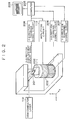
- Figs. 5 and 6 show conventional AFMs. Basically, an AFM is composed of a
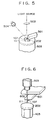
probe 111 opposed to the specimen surface, acantilever 107 supporting the probe, a means for detecting the amount of displacement of the cantilever due to the atomic force acting between the specimen and the probe, and a means for three-dimensionally controlling the relative position of the specimen with respect to the probe. - In the conventional AFM shown in Fig. 5, the detection of cantilever displacement amount is effected by an optical lever method according to which a light beam is applied from behind the
cantilever 107, obtaining the displacement amount from the shift amount of the position of the reflected-light spot. In the conventional AFM shown in Fig. 6, a tunnel-current method is adopted, according to which aconductive probe 602 is arranged behind thecantilever 107 at a position close to it, and position control is performed on theconductive probe 602 in such a manner that the tunnel current flowing between thecantilever 107 and theconductive probe 602 is maintained constant, obtaining the displacement amount of the cantilever from the position control amount. - However, the optical lever method, described above, requires an adjusting jig for causing the light beam to be applied to the back surface of the cantilever, an optical component such as a
lens 502 or a mirror, and a position adjusting jig for a half-split photodiode 504. The tunnel current method requires a jig for adjusting the position of theconductive probe 602 with respect to the back surface of the cantilever. Thus, in both methods, the mechanical structure of the cantilever displacement amount detecting means has to be rather large and complicated. As a result, the mechanical structure of the displacement amount detecting means is subject to positional deviation due to disturbances such as floor vibration, acoustic vibration, or temperature drift, or to generation of resonance due to deterioration in rigidity, thus making it difficult for the detection of the cantilever displacement amount to be effected at a satisfactory level of resolution. - It is an object of the present invention to provide a cantilever unit in which the cantilever displacement amount detecting means is integrated with the cantilever and which is little subject to the influence of disturbances.
- Another object of the present invention is provide an AFM which uses such a novel cantilever unit and which requires no relative positioning and is little subject to the influence of disturbances. Still another object of the present invention is to provide a reproducing apparatus utilizing this AFM to reproduce information recorded on a recording medium, as well as an information processing apparatus in which this AFM is combined with an STM.
- In a first aspect of the present invention, there is provided a cantilever unit comprising a cantilever for supporting a probe and a displacement amount detecting means, which displacement amount detecting means is integrated with the cantilever.
- In a second aspect of the present invention, there is provided an information processing apparatus, comprising a cantilever unit according to the first aspect of the present invention.
- In a third aspect of the present invention, there is provided an information processing apparatus, comprising a cantilever unit according to the first aspect of the present invention and an information recording medium stationed in close vicinity to said unit, wherein an information in the medium is reproduced at a signal on the basis of an displacement amount of the cantilever.
- In a fourth aspect of the present invention, there is provided an atomic force microscope comprising a cantilever unit according to the first aspect of the present invention.
- In a fifth aspect of the present invention, there is provided a magnetic force microscope comprising a cantilever unit according to the first aspect of the present invention.
- In accordance with the present invention, the optical-integrated-circuit technique is utilized to optically integrate a light source, an optical waveguide, a waveguide-type optical-path changing device and a photodetector into one integral detection unit, which is integrated with a cantilever, thereby making it possible to reduce the size of the displacement detecting means to 1/50 or less as compared to that used in conventional AFMs. Accordingly, the resonance frequency of the detecting means can be increased to a value several tens times larger than that in the conventional AFMs, thus rendering the detecting means little subject to the influence of disturbances.
- More specifically, optical components, such as a light source, an optical waveguide, a lens for condensing the light in the optical waveguide, a beam splitter for dividing or synthesizing a light beam, a mirror for turning the direction of light, and optical parts such as a coupler for extracting light out of the waveguide, a photodiode for detecting light quantity, a photoelectric-current amplifying circuit, a signal processing circuit, etc. are integrated into one unit, which is integrated with a cantilever.
-
- Fig. 1 is a diagram showing the construction of an optically integrated cantilever unit according to a first embodiment of the present invention.
- Fig. 2 is a diagram showing the construction of an atomic force microscope using the optically integrated cantilever unit according to the first embodiment of the present invention;
- Fig. 3 is a diagram showing the construction of an optically integrated cantilever unit according to a second embodiment of the present invention;
- Fig. 4 is a diagram showing the construction of a cantilever unit applied to an information processing apparatus according to the other embodiment of the present invention;
- Fig. 5 is a diagram showing a prior-art example of a cantilever displacement amount detecting system in an atomic force microscope; and
- Fig. 6 is a diagram showing another prior-art example of a cantilever displacement amount detecting system in an atomic force microscope.
- The present invention will now be described in more detail with reference to embodiments thereof.
- Fig. 1 shows the construction of a cantilever unit according to an embodiment of the present invention.
- The cantilever unit shown includes a film
optical waveguide 101, an SiO2 layer 102, anSi substrate 103, asemiconductor laser 104, a Fresnellens 105, agrating beam splitter 106, acantilever 107, a reflecting mirror (a) indicated at 108, a reflecting mirror (b) indicated at 109, aphotodiode 110, aprobe 111, a semiconductorlaser driving circuit 112, and an amplifyingcircuit 113. - In this embodiment, the
semiconductor laser 104 is joined to one end surface of the SiO2/Si substrate 103, on the surface of which is formed the filmoptical waveguide 101, and serves to introduce a laser beam into theoptical waveguide 101. The introduced laser beam is collimated by the Fresnellens 105, and is then separated into two rays in different directions by thegrating beam splitter 106. One of the rays, indicated by the symbol A, passes through the optical waveguide provided on the surface of thecantilever 107 that is provided on the other end surface of theSi substrate 103, and is reflected by the reflecting mirror (a), 108, which is provided on the free-end surface of thecantilever 107, to pass backwards through the optical waveguide on the surface of thecantilever 107 before it enters thegrating beam splitter 106 again. - The other ray of light, indicated by the symbol B, whose course has been turned by 90°, is reflected by the reflecting mirror (b), 109, and is transmitted through the same course backwardly before it enters the
grating beam splitter 106 again. The two rays are then synthesized by thegrating beam splitter 106 into a synthesized light C, which is detected by thephotodiode 110. When theprobe 111 provided on thecantilever 107 detects an atomic force to cause the tip end section of thecantilever 107 to be flexed in the Z-direction in the drawing, a distortion corresponding to the displacement amount ΔZ is generated in the optical waveguide on the surface of thecantilever 107, thereby changing the refractive index of the optical waveguide. Assuming that this change in refractive index is Δn,
cantilever 107, and the ray of light B, which is reflected by the reflectingmirror 109, resulting in a change in the luminous intensity of the synthesized light C. Therefore, by detecting this change in luminous intensity, it is possible to detect the displacement amount in the Z-direction, ΔZ, of the tip end section of thecantilever 107. A signal indicative of this change in luminous intensity is amplified by the amplifyingcircuit 113 to become a Z-direction displacement signal. Assuming that the elastic constant in the Z-direction of thecantilever 107 is k, the magnitude f of the atomic force detected by theprobe 111 can be obtained by the equation:
- A method of preparing such an optically integrated cantilever unit will now be described.
- A PiN photodiode is formed on an Si substrate by the usual silicon processing. Then, a protective Si3N4 film having a thickness of 0.1 µm is formed thereon by the LPCVD method. Next, after forming an SiO2 film having a thickness of 0.5 µm by thermal oxidation on other opening sections, the Si3N4 film is removed by plasma etching. Subsequently, an As2S3 film optical waveguide having a thickness of 1 µm is formed on the SiO2 film by vacuum evaporation, and, by utilizing the change in refractive index by electron beam irradiation, a Fresnel lens and a grating beam splitter are formed in the optical waveguide. After patterning of configuration of a cantilever, anisotropic etching is performed from the back side of the substrate by using KOH solution, thereby forming the cantilever. Then, a probe is provided at the tip end of the cantilever by the electron beam deposition method. After performing cleavage on the chip thus obtained, a metal such as Al is deposited on one end surface thereof and on a side surface of the tip end portion of the cantilever to form reflecting mirrors, and a semiconductor laser is joined to the other end surface.
- Next, the AFM of the present invention, constructed by using the optical integrated cantilever unit shown in Fig. 1, will be described with reference to Fig. 2. A
specimen 202 opposed tocantilever unit 201 of the type shown in Fig. 1 is brought near to theprobe 111 of the unit by means of an XYZ-drive device 203, up to a position at a distance of 1nm or less therefrom. Due to the atomic force acting between theprobe 111 and the surface of thespecimen 202, a deflection is generated in the cantilever. A Z-direction feedback signal is supplied to the XYZ-drive device 203 such that the amount of this deflection is kept constant (i.e., the atomic force is kept constant), thereby controlling the distance between theprobe 111 and thespecimen 202. Further, a scanning signal is supplied from acomputer 205. On the basis of this scanning signal, an X-direction scanning signal and a Y-direction scanning signal are supplied to the XYZ-drive device 203 by an X-directionscanning signal circuit 206 and a Y-directionscanning signal circuit 207, respectively, thereby scanning thespecimen 202 in the XYZ-dimensions relative to theprobe 111. In this process, it is possible to detect the depth or height of the surface irregularities from the Z-direction feedback signal for keeping the deflection amount of the cantilever constant. In thecomputer 205, two-dimensional distribution data on the surface irregularities is obtained. The data is displayed on adisplay 209. When a magnetic substance, such as Fe, Co or Ni, is used here as the material of the probe, a magnetic force microscope is obtained, which makes it possible to observe the magnetic domain structure of the surface of a magnetic specimen. - Fig. 3 shows the construction of an optically integrated cantilever unit according to a second embodiment of the present invention. The cantilever unit shown includes an SiO2/Si substrate (102'/103') having on its surface a film
optical waveguide 101, into which a laser beam is introduced from asemiconductor laser 112 joined to one end surface of the substrate. The laser beam introduced is collimated by a Fresnel lens 305, and is then reflected by a reflecting mirror (c) indicated at 306 before it enters a grating coupler (a) indicated at 307. In the grating coupler (a), 307, part of the light is extracted out of the optical waveguide, as indicated by the symbol A, and is reflected by the back surface of thecantilever 107. After that, the part of the light returns to the optical waveguide at a grating coupler (b), indicated at 309, to be synthesized with the ray of light B which has been propagated through the optical waveguide, thus becoming a synthesized light C, which is reflected by a reflected mirror (d), indicated at 310, and then detected by thephotodiode 110. When theprobe 111 provided on thecantilever 107 detects an atomic force and causes the tip end section of thecantilever 107 to be deflected in the Z-direction in the drawing, there is generated, in accordance with the displacement amount ΔZ of the cantilever, a change in the length of the optical path through which the light portion A, extracted out of the optical waveguide at the grating coupler (a), 307, returns to the optical waveguide at the grating coupler (b), 309. Assuming that this change is ΔE, there is generated, in the optical path difference between the light A extracted out of the optical waveguide and the light B which has been propagated through the optical waveguide, a change
cantilever 107. A signal indicative of this change in luminous intensity is amplified by the amplifyingcircuit 113 to become a Z-direction displacement amount signal. Assuming that the elastic constant in the Z-direction of thecantilever 107 is k, the magnitude f of the atomic force detected by theprobe 111 can be obtained from the equation:
- Next, a method of producing the optical integrated cantilever unit of this embodiment will be described.
- A PiN photodiode is formed on an Si substrate by the usual silicon processing. Then, a protective Si3N4 film having a thickness of 0.1 µm is formed thereon by the LPCVD method. Next, after forming an SiO2 film having a thickness of 2.5 µm by thermal oxidation on other opening sections, the SiO2 film is removed by plasma etching. Subsequently, a glass-film optical waveguide of 7059 Glass (manufactured by Corning) having a thickness of 2 µm is formed on the SiO2 film by high-frequency sputtering, and, by utilizing the change in refractive index by ion exchange, ion implanation or the like, a Fresnel lens and grating couplers are formed. Then, a chip having a cantilever formed by patterning and anisotropic etching on another Si substrate is joined to the glass-film optical waveguide by anode bonding method. After performing cleavage and polishing on the chip, a metal such as Al is deposited on end surfaces thereof to form reflecting mirrors, and a semiconductor laser is joined to another end surface thereof.
- Referring to Fig. 4, embodiment of information processing (recording/reproducing) apparatus of the present invention will be described in the following. The same constitution of apparatus (not illustrated) as in the above Fig. 2 is employed in the present embodiment, too. In Fig. 4,
probe 111 is formed of a conductive material. Further, the cantilever unit is arranged so that a tip of the probe is close to a desired position on the surface of the information recording medium (not illustrated), which corresponds to thespecimen 202 in Fig. 2. - Voltage for recording is applied between
probe 111 and the above-mentioned medium by voltage applying circuit for recording, to form a bit on the desired position of the above-mentioned medium.Reference numeral 317 indicates an Al wiring. - In the present invention, a material capable of changing a form of own surface by current flowing through the part was employed as medium as mentioned above.
- The operation reproducing the bits (information) recorded on the above-mentioned medium in such a manner is described below. The tip of the
probe 111 is stationed in close vicinity to the surface of the above-mentioned medium, and theprobe 111 is scanned in a x-y direction in the figure. When the tip of theprobe 111 is made opposite to the above-mentioned bit, the tip is stressed according to the shape of the bit, wherebycantilever 107 is flexed. The amount of flex is detected by the above-mentioned displacement amount detecting means in the cantilever unit of the present invention, to obtain the reproducing signal. - As mentioned above, the apparatus where the recording of information is done by application of the STM constitution and the reproducting of the information is done by application of the AFM constituion was explained.
- As described above, in accordance with this invention, the cantilever displacement amount detecting system is formed as an integrated unit, which is integrated with the cantilever, thereby providing the following advantages:
- (1) No relative positioning of the cantilever and the displacement amount detecting system is needed, thus attaining an improvement in maneuverability; and
- (2) The apparatus as a whole can be reduced in size and rendered less subject to the influence of disturbances, thereby attaining an improvement in detecting resolution and making it possible to measure the three-dimensional surface configuration of a specimen with an AFM of higher accuracy and higher resolution.
Claims (28)
- A cantilever unit comprising a cantilever for supporting a probe and a displacement amount detecting means, said displacement amount detecting means being integrated with said cantilever.
- A cantilever unit according to claim 1, wherein said displacement amount detecting means is comprised of a light source, an optical waveguide, a waveguide-type optical-path changing device, and a photo detecting device.
- A cantilever unit according to claim 1, wherein said displacement amount detecting means consists of an optically integrated unit comprised of plural optical parts.
- A cantilever unit according to claim 1, wherein said cantilever is comprised of a layer product comprised of a Si substrate and a SiO2 layer.
- A cantilever unit according to claim 2, wherein said optical waveguide is laminated to said cantilever.
- A cantilever unit according to claim 2, wherein said light source is a semiconductor laser.
- A cantilever unit according to claim 2, wherein said photo detecting device is a photodiode.
- A cantilever unit according to claim 1, which unit further has an optical current amplifying circuit.
- A cantilever unit according to claim 1, which unit further has a signal processing circuit.
- An information processing apparatus, comprising a cantilever unit of any of claims 1 through 9.
- An information processing apparatus, comprising a cantilever unit of any of claims 1 through 9 and an information recording medium stationed in close vicinity to said unit, wherein an information in said medium is reproduced at a signal on the basis of an displacement amount of said cantilever.
- An information processing apparatus according to claim 11, which apparatus comprises a means applying an voltage between a probe in said unit and said medium.
- An information processing apparatus according to claim 12, which apparatus records an information in said medium by tunnel current.
- An atomic force microscope comprising a cantilever unit of any of claims 1 through 9.
- An magnetic force microscope comprising a cantilever unit of any of claims 1 through 9.
- A magnetic force microscope according to claim 15, wherein a probe in said unit is comprised of a magnetic substance.
- An information processing apparatus, comprising a probe (111) being adapted to oppose in operation a surface of a specimen (202), a cantilever means (107) for supporting the probe and a detecting means for detecting displacement of the cantilever means (107), the apparatus being arranged to detect information in the surface of said specimen (202) based on the displacement amount detected by the detecting means;
said apparatus being arranged such that the detecting means is integrated with the cantilever means (107) and comprises:a semiconductor laser light source (104);means (105) for collimating the laser light emitted from the light source (104);an optical waveguide (101) for guiding the laser light;means (106,307,309) for dividing and synthesizing the laser light in order to form a ray of light, the intensity of which changes according to the amount of displacement of the cantilever means (107); anda photodetector (110) arranged to receive the ray of light. - An apparatus according to claim 17, wherein said means for dividing and synthesizing the laser light is a grating beam splitter (106).
- An apparatus according to claim 17, wherein said means for dividing and synthesizing the laser light is a plurality of grating couplers (307,309).
- An apparatus according to claim 17, wherein said apparatus is an atomic force microscope.
- An apparatus according to claim 17, wherein said probe (111) comprises a magnetic material.
- An apparatus according to claim 21, wherein said apparatus is a magnetic force microscope.
- An apparatus according to claim 17, wherein said apparatus is an information reproducing apparatus.
- An apparatus according to claim 17, wherein said apparatus further comprises means for applying a voltage between the specimen (202) and the probe (111).
- An apparatus according to claim 24, wherein said apparatus is an information recording and reproducing apparatus.
- An apparatus according to claim 17, wherein the optical components of the detecting means are optically integrated with the cantilever means (107).
- A cantilever unit comprising:a probe (111),a cantilever means (107) for supporting the probe and a detecting means for detecting displacement of the cantilever means,characterised in that said unit being arranged such that the detecting means is integrated with the cantilever means and comprises:a semiconductor laser light source (104);means (105) for collimating the laser light emitted from the light source;an optical waveguide (101) for guiding the laser light;means (106, 307, 309) for dividing and synthesizing the laser light in order to form a ray of light, the intensity of which changes according to the amount of displacement of the cantilever means; anda photodetector (110) arranged to receive the ray of light.
- A cantilever unit according to claim 27, wherein the optical components of the detecting means are optically integrated with the cantilever means (107).
Applications Claiming Priority (4)
| Application Number | Priority Date | Filing Date | Title |
|---|---|---|---|
| JP10363491 | 1991-04-10 | ||
| JP3103634A JP3000491B2 (en) | 1991-04-10 | 1991-04-10 | Cantilever unit, information processing apparatus using the same, atomic force microscope, magnetic force microscope |
| JP103634/91 | 1991-04-10 | ||
| EP92303177A EP0509716A1 (en) | 1991-04-10 | 1992-04-09 | Cantilever unit and atomic force microscope, magnetic force microscope, reproducing apparatus and information processing apparatus using the cantilever unit |
Related Parent Applications (2)
| Application Number | Title | Priority Date | Filing Date |
|---|---|---|---|
| EP92303177A Division EP0509716A1 (en) | 1991-04-10 | 1992-04-09 | Cantilever unit and atomic force microscope, magnetic force microscope, reproducing apparatus and information processing apparatus using the cantilever unit |
| EP92303177.7 Division | 1992-04-09 |
Publications (3)
| Publication Number | Publication Date |
|---|---|
| EP0791803A2 true EP0791803A2 (en) | 1997-08-27 |
| EP0791803A3 EP0791803A3 (en) | 1997-10-22 |
| EP0791803B1 EP0791803B1 (en) | 2002-01-09 |
Family
ID=14359206
Family Applications (2)
| Application Number | Title | Priority Date | Filing Date |
|---|---|---|---|
| EP97200263A Expired - Lifetime EP0791803B1 (en) | 1991-04-10 | 1992-04-09 | Cantilever unit and atomic force microscope, magnetic force microscope, reproducing apparatus and information processing apparatus using the cantilever unit |
| EP92303177A Withdrawn EP0509716A1 (en) | 1991-04-10 | 1992-04-09 | Cantilever unit and atomic force microscope, magnetic force microscope, reproducing apparatus and information processing apparatus using the cantilever unit |
Family Applications After (1)
| Application Number | Title | Priority Date | Filing Date |
|---|---|---|---|
| EP92303177A Withdrawn EP0509716A1 (en) | 1991-04-10 | 1992-04-09 | Cantilever unit and atomic force microscope, magnetic force microscope, reproducing apparatus and information processing apparatus using the cantilever unit |
Country Status (6)
| Country | Link |
|---|---|
| US (1) | US5260567A (en) |
| EP (2) | EP0791803B1 (en) |
| JP (1) | JP3000491B2 (en) |
| AT (1) | ATE211814T1 (en) |
| CA (1) | CA2065593C (en) |
| DE (1) | DE69232339T2 (en) |
Cited By (4)
| Publication number | Priority date | Publication date | Assignee | Title |
|---|---|---|---|---|
| WO2004112050A1 (en) * | 2003-06-18 | 2004-12-23 | Atilla Aydinli | Integrated optical displacement sensors for scanning probe microscopy |
| CN109884562A (en) * | 2019-03-29 | 2019-06-14 | 中国电子产品可靠性与环境试验研究所((工业和信息化部电子第五研究所)(中国赛宝实验室)) | Difference magnetic field detection module and magnet field probe |
| CN109884561A (en) * | 2019-03-29 | 2019-06-14 | 中国电子产品可靠性与环境试验研究所((工业和信息化部电子第五研究所)(中国赛宝实验室)) | Magnetic field detection module and magnet field probe |
| CN110095656A (en) * | 2019-05-27 | 2019-08-06 | 中国电子产品可靠性与环境试验研究所((工业和信息化部电子第五研究所)(中国赛宝实验室)) | Detecting module and probe |
Families Citing this family (58)
| Publication number | Priority date | Publication date | Assignee | Title |
|---|---|---|---|---|
| US5155361A (en) * | 1991-07-26 | 1992-10-13 | The Arizona Board Of Regents, A Body Corporate Acting For And On Behalf Of Arizona State University | Potentiostatic preparation of molecular adsorbates for scanning probe microscopy |
| JPH05282717A (en) * | 1992-03-31 | 1993-10-29 | Canon Inc | Manufacture of recording medium, and recording medium and information processor |
| DE4310349C2 (en) * | 1993-03-30 | 2000-11-16 | Inst Mikrotechnik Mainz Gmbh | Sensor head and method for its production |
| DE69433974T2 (en) * | 1993-04-13 | 2005-09-01 | Agilent Technologies, Inc., Palo Alto | ELECTRO-OPTICAL INSTRUMENT |
| DE59302118D1 (en) * | 1993-05-21 | 1996-05-09 | Heidenhain Gmbh Dr Johannes | Photoelectric position measuring device |
| US5504338A (en) * | 1993-06-30 | 1996-04-02 | The United States Of America As Represented By The Secretary Of The Navy | Apparatus and method using low-voltage and/or low-current scanning probe lithography |
| JP3390173B2 (en) * | 1993-07-22 | 2003-03-24 | ビーティージー・インターナショナル・リミテッド | Intelligent sensors for near-field optical devices |
| US5440920A (en) * | 1994-02-03 | 1995-08-15 | Molecular Imaging Systems | Scanning force microscope with beam tracking lens |
| US5515719A (en) * | 1994-05-19 | 1996-05-14 | Molecular Imaging Corporation | Controlled force microscope for operation in liquids |
| US5866805A (en) * | 1994-05-19 | 1999-02-02 | Molecular Imaging Corporation Arizona Board Of Regents | Cantilevers for a magnetically driven atomic force microscope |
| US5753814A (en) * | 1994-05-19 | 1998-05-19 | Molecular Imaging Corporation | Magnetically-oscillated probe microscope for operation in liquids |
| US5513518A (en) * | 1994-05-19 | 1996-05-07 | Molecular Imaging Corporation | Magnetic modulation of force sensor for AC detection in an atomic force microscope |
| US5621210A (en) * | 1995-02-10 | 1997-04-15 | Molecular Imaging Corporation | Microscope for force and tunneling microscopy in liquids |
| JPH0981977A (en) * | 1995-07-10 | 1997-03-28 | Canon Inc | Recording and reproducing device |
| JP3679519B2 (en) * | 1995-09-14 | 2005-08-03 | キヤノン株式会社 | Manufacturing method of micro tip for detecting tunnel current or micro force or magnetic force, manufacturing method of probe having the micro tip, probe thereof, probe unit having the probe, scanning probe microscope, and information recording / reproducing apparatus |
| US5874668A (en) * | 1995-10-24 | 1999-02-23 | Arch Development Corporation | Atomic force microscope for biological specimens |
| JP3260619B2 (en) * | 1996-03-19 | 2002-02-25 | セイコーインスツルメンツ株式会社 | Optical waveguide probe and optical system |
| JPH10293134A (en) | 1997-02-19 | 1998-11-04 | Canon Inc | Optical detection or irradiation probe, near field optical microscope, recorder/placer and aligner employing it, and manufacture of probe |
| US5982009A (en) * | 1997-03-01 | 1999-11-09 | Korea Advanced Institute Of Science & Technology | Integrated device of cantilever and light source |
| JPH10312592A (en) * | 1997-05-13 | 1998-11-24 | Canon Inc | Information processor and processing method |
| JP2000035396A (en) | 1998-07-16 | 2000-02-02 | Canon Inc | Probe with minute protrusion and its manufacturing method |
| US7260051B1 (en) | 1998-12-18 | 2007-08-21 | Nanochip, Inc. | Molecular memory medium and molecular memory integrated circuit |
| US20030160170A1 (en) * | 2000-03-30 | 2003-08-28 | Mcmaster Terence J. | Methods and apparatus for atomic force microscopy |
| JP2003077154A (en) * | 2001-04-25 | 2003-03-14 | Olympus Optical Co Ltd | Mirror angle detector, optical signal switching system and method |
| JP2003202284A (en) * | 2002-01-09 | 2003-07-18 | Hitachi Ltd | Scanning probe microscope, and sample observing method and method of manufacturing device by using the same |
| US7233517B2 (en) | 2002-10-15 | 2007-06-19 | Nanochip, Inc. | Atomic probes and media for high density data storage |
| US20040150472A1 (en) * | 2002-10-15 | 2004-08-05 | Rust Thomas F. | Fault tolerant micro-electro mechanical actuators |
| US6982898B2 (en) * | 2002-10-15 | 2006-01-03 | Nanochip, Inc. | Molecular memory integrated circuit utilizing non-vibrating cantilevers |
| US6985377B2 (en) | 2002-10-15 | 2006-01-10 | Nanochip, Inc. | Phase change media for high density data storage |
| US6821941B2 (en) * | 2002-10-23 | 2004-11-23 | Isp Investments Inc. | Tablet of compacted particulated cleaning composition |
| JP2004301554A (en) * | 2003-03-28 | 2004-10-28 | Canon Inc | Electric potential measuring device and image forming device |
| US7379412B2 (en) | 2004-04-16 | 2008-05-27 | Nanochip, Inc. | Methods for writing and reading highly resolved domains for high density data storage |
| US20050232061A1 (en) | 2004-04-16 | 2005-10-20 | Rust Thomas F | Systems for writing and reading highly resolved domains for high density data storage |
| US7301887B2 (en) | 2004-04-16 | 2007-11-27 | Nanochip, Inc. | Methods for erasing bit cells in a high density data storage device |
| US8601608B2 (en) * | 2005-03-31 | 2013-12-03 | Japan Science And Technology Agency | Cantilever for scanning probe microscope and scanning probe microscope equipped with it |
| US7552625B2 (en) * | 2005-06-17 | 2009-06-30 | Georgia Tech Research Corporation | Force sensing integrated readout and active tip based probe microscope systems |
| US20070103697A1 (en) * | 2005-06-17 | 2007-05-10 | Degertekin Fahrettin L | Integrated displacement sensors for probe microscopy and force spectroscopy |
| US7463573B2 (en) | 2005-06-24 | 2008-12-09 | Nanochip, Inc. | Patterned media for a high density data storage device |
| US7367119B2 (en) | 2005-06-24 | 2008-05-06 | Nanochip, Inc. | Method for forming a reinforced tip for a probe storage device |
| US7309630B2 (en) | 2005-07-08 | 2007-12-18 | Nanochip, Inc. | Method for forming patterned media for a high density data storage device |
| US7441447B2 (en) * | 2005-10-07 | 2008-10-28 | Georgia Tech Research Corporation | Methods of imaging in probe microscopy |
| US7752898B2 (en) * | 2005-10-28 | 2010-07-13 | Georgia Tech Research Corporation | Devices for probe microscopy |
| US7797757B2 (en) * | 2006-08-15 | 2010-09-14 | Georgia Tech Research Corporation | Cantilevers with integrated actuators for probe microscopy |
| KR100889976B1 (en) * | 2006-10-24 | 2009-03-24 | 이형종 | Optical module and optical sensor using the same and method for manufacturing thereof |
| US9391216B2 (en) * | 2008-06-06 | 2016-07-12 | Orbital Atk, Inc. | Optical coupled sensors for harsh environments |
| US9217831B1 (en) * | 2009-12-15 | 2015-12-22 | Kotura, Inc. | Optical system having dynamic waveguide alignment |
| CN101876667A (en) * | 2010-06-30 | 2010-11-03 | 北京大学 | Atomic force microscope probe based on structures of carbon nano tube and planar wave guide |
| US20130205455A1 (en) * | 2012-02-07 | 2013-08-08 | University Of Western Australia | System and method of performing atomic force measurements |
| US9835591B2 (en) | 2011-02-25 | 2017-12-05 | Panorama Synergy Ltd | Optical cantilever based analysis |
| US9057706B2 (en) | 2011-02-25 | 2015-06-16 | University Of Western Australia | Optical cantilever based analyte detection |
| GB2493585B (en) * | 2011-08-11 | 2013-08-14 | Ibm | Scanning probe microscopy cantilever comprising an electromagnetic sensor |
| US9977188B2 (en) | 2011-08-30 | 2018-05-22 | Skorpios Technologies, Inc. | Integrated photonics mode expander |
| FR3007589B1 (en) * | 2013-06-24 | 2015-07-24 | St Microelectronics Crolles 2 | PHOTONIC INTEGRATED CIRCUIT AND METHOD OF MANUFACTURE |
| EP3149522A4 (en) * | 2014-05-27 | 2018-02-21 | Skorpios Technologies, Inc. | Waveguide mode expander using amorphous silicon |
| US9857216B2 (en) * | 2014-12-26 | 2018-01-02 | Ricoh Company, Ltd. | Minute object characteristics measuring apparatus |
| JP6766351B2 (en) * | 2014-12-26 | 2020-10-14 | 株式会社リコー | Micro object characteristic measuring device |
| WO2016160909A1 (en) * | 2015-03-31 | 2016-10-06 | University Of Kansas | Scanning resonator microscopy |
| EP3722741A1 (en) * | 2019-04-08 | 2020-10-14 | Nokia Technologies Oy | An apparatus comprising a cantilever |
Family Cites Families (15)
| Publication number | Priority date | Publication date | Assignee | Title |
|---|---|---|---|---|
| US3837728A (en) * | 1973-09-26 | 1974-09-24 | Bell Telephone Labor Inc | Injected carrier guided wave deflector |
| US4724318A (en) * | 1985-11-26 | 1988-02-09 | International Business Machines Corporation | Atomic force microscope and method for imaging surfaces with atomic resolution |
| DE3630887A1 (en) * | 1986-03-26 | 1987-10-08 | Hommelwerke Gmbh | DEVICE FOR MEASURING SMALL LENGTHS |
| EP0242407A2 (en) * | 1986-03-26 | 1987-10-28 | Hommelwerke GmbH | Device for measuring small lengths |
| EP0262253A1 (en) * | 1986-10-03 | 1988-04-06 | International Business Machines Corporation | Micromechanical atomic force sensor head |
| FR2613826B1 (en) * | 1987-04-07 | 1990-10-26 | Commissariat Energie Atomique | MOTION SENSOR IN INTEGRATED OPTICS |
| DE3750406T2 (en) * | 1987-05-12 | 1995-03-30 | Ibm | Atomic force sensor with interferometric measurement of the properties of a data carrier. |
| DE3718192A1 (en) * | 1987-05-29 | 1988-12-08 | Hommelwerke Gmbh | DEVICE FOR MEASURING THE DISTANCE BETWEEN THE DEVICE AND A MEASURING AREA |
| JPH02503713A (en) * | 1987-06-04 | 1990-11-01 | ルコツ バルター | Optical modulation and measurement methods |
| US4906840A (en) * | 1988-01-27 | 1990-03-06 | The Board Of Trustees Of Leland Stanford Jr., University | Integrated scanning tunneling microscope |
| JP2547869B2 (en) * | 1988-11-09 | 1996-10-23 | キヤノン株式会社 | PROBE UNIT, METHOD FOR DRIVING THE PROBE, AND SCANNING TUNNEL CURRENT DETECTION DEVICE HAVING THE PROBE UNIT |
| JPH02187944A (en) * | 1989-01-13 | 1990-07-24 | Sharp Corp | Reproducing device |
| US5017010A (en) * | 1989-05-16 | 1991-05-21 | International Business Machines Corporation | High sensitivity position sensor and method |
| JPH04188022A (en) * | 1990-11-22 | 1992-07-06 | Olympus Optical Co Ltd | Displacement detecting apparatus |
| DE4107605C1 (en) * | 1991-03-09 | 1992-04-02 | Hommelwerke Gmbh, 7730 Villingen-Schwenningen, De | Sensor for atomic force raster microscope - has opto-electronic distance measurer for ascertaining movement of probe tip at distal end of extendable arm |
-
1991
- 1991-04-10 JP JP3103634A patent/JP3000491B2/en not_active Expired - Fee Related
-
1992
- 1992-04-08 US US07/865,227 patent/US5260567A/en not_active Expired - Fee Related
- 1992-04-08 CA CA002065593A patent/CA2065593C/en not_active Expired - Fee Related
- 1992-04-09 AT AT97200263T patent/ATE211814T1/en not_active IP Right Cessation
- 1992-04-09 EP EP97200263A patent/EP0791803B1/en not_active Expired - Lifetime
- 1992-04-09 EP EP92303177A patent/EP0509716A1/en not_active Withdrawn
- 1992-04-09 DE DE69232339T patent/DE69232339T2/en not_active Expired - Fee Related
Non-Patent Citations (1)
| Title |
|---|
| None |
Cited By (4)
| Publication number | Priority date | Publication date | Assignee | Title |
|---|---|---|---|---|
| WO2004112050A1 (en) * | 2003-06-18 | 2004-12-23 | Atilla Aydinli | Integrated optical displacement sensors for scanning probe microscopy |
| CN109884562A (en) * | 2019-03-29 | 2019-06-14 | 中国电子产品可靠性与环境试验研究所((工业和信息化部电子第五研究所)(中国赛宝实验室)) | Difference magnetic field detection module and magnet field probe |
| CN109884561A (en) * | 2019-03-29 | 2019-06-14 | 中国电子产品可靠性与环境试验研究所((工业和信息化部电子第五研究所)(中国赛宝实验室)) | Magnetic field detection module and magnet field probe |
| CN110095656A (en) * | 2019-05-27 | 2019-08-06 | 中国电子产品可靠性与环境试验研究所((工业和信息化部电子第五研究所)(中国赛宝实验室)) | Detecting module and probe |
Also Published As
| Publication number | Publication date |
|---|---|
| DE69232339T2 (en) | 2002-08-08 |
| CA2065593A1 (en) | 1992-10-11 |
| CA2065593C (en) | 1999-01-19 |
| EP0791803A3 (en) | 1997-10-22 |
| EP0509716A1 (en) | 1992-10-21 |
| ATE211814T1 (en) | 2002-01-15 |
| EP0791803B1 (en) | 2002-01-09 |
| JPH04311839A (en) | 1992-11-04 |
| JP3000491B2 (en) | 2000-01-17 |
| US5260567A (en) | 1993-11-09 |
| DE69232339D1 (en) | 2002-02-14 |
Similar Documents
| Publication | Publication Date | Title |
|---|---|---|
| US5260567A (en) | Cantilever unit and atomic force microscope, magnetic force microscope, reproducing apparatus and information processing apparatus using the cantilever unit | |
| JP3000492B2 (en) | Information processing device | |
| US5231286A (en) | Scanning probe microscope utilizing an optical element in a waveguide for dividing the center part of the laser beam perpendicular to the waveguide | |
| US6046972A (en) | Method and producing probe with minute aperture, scanning near-field optical microscope using the probe and recording and/or reproducing apparatus using the probe | |
| US6785445B2 (en) | Near field light probe, near field optical microscope, near field light lithography apparatus, and near field light storage apparatus that have the near field light probe | |
| US7323684B2 (en) | Scanning probe microscope and specimen observation method and semiconductor device manufacturing method using said scanning probe microscope | |
| US5274230A (en) | Scanning probe microscope having first and second optical waveguides | |
| JP3069923B2 (en) | Cantilever probe, atomic force microscope, information recording / reproducing device | |
| US6376827B1 (en) | Near field optical memory head | |
| JP3161116B2 (en) | Micro gap width measuring apparatus and method | |
| Baida et al. | Combination of a fiber and a silicon nitride tip as a bifunctional detector; first results and perspectives | |
| Egawa et al. | High‐speed scanning by dual feedback control in SNOM/AFM | |
| US6689545B2 (en) | Method of fabricating near-field light-generating element | |
| EP1115113A1 (en) | Information recording medium, information reproducing device, and information recording/reproducing device | |
| US6587426B1 (en) | Recording medium having information reproducible using near-field light | |
| US20030206513A1 (en) | Optical element, optical head and signal reproducing method | |
| JPH085642A (en) | Integrated multifunction spm sensor | |
| JPH06258068A (en) | Interatomic force microscope | |
| JP3242787B2 (en) | Photon scanning tunneling microscope | |
| JP2694783B2 (en) | Atomic force microscope | |
| JP2962612B2 (en) | Scanning microscope | |
| JPH05231861A (en) | Scanning probe microscope | |
| de Fornel | Micro-Aperture Microscopy | |
| JPH11238244A (en) | Optical memory | |
| Iams | Atomic force microscopy of magnetic samples using optical detection methods |
Legal Events
| Date | Code | Title | Description |
|---|---|---|---|
| PUAI | Public reference made under article 153(3) epc to a published international application that has entered the european phase |
Free format text: ORIGINAL CODE: 0009012 |
|
| AC | Divisional application: reference to earlier application |
Ref document number: 509716 Country of ref document: EP |
|
| AK | Designated contracting states |
Kind code of ref document: A2 Designated state(s): AT BE CH DE DK ES FR GB GR IT LI LU NL PT SE |
|
| PUAL | Search report despatched |
Free format text: ORIGINAL CODE: 0009013 |
|
| AK | Designated contracting states |
Kind code of ref document: A3 Designated state(s): AT BE CH DE DK ES FR GB GR IT LI LU NL PT SE |
|
| 17P | Request for examination filed |
Effective date: 19980304 |
|
| 17Q | First examination report despatched |
Effective date: 20000107 |
|
| GRAG | Despatch of communication of intention to grant |
Free format text: ORIGINAL CODE: EPIDOS AGRA |
|
| GRAG | Despatch of communication of intention to grant |
Free format text: ORIGINAL CODE: EPIDOS AGRA |
|
| GRAH | Despatch of communication of intention to grant a patent |
Free format text: ORIGINAL CODE: EPIDOS IGRA |
|
| GRAH | Despatch of communication of intention to grant a patent |
Free format text: ORIGINAL CODE: EPIDOS IGRA |
|
| GRAA | (expected) grant |
Free format text: ORIGINAL CODE: 0009210 |
|
| REG | Reference to a national code |
Ref country code: GB Ref legal event code: IF02 |
|
| AC | Divisional application: reference to earlier application |
Ref document number: 509716 Country of ref document: EP |
|
| AK | Designated contracting states |
Kind code of ref document: B1 Designated state(s): AT BE CH DE DK ES FR GB GR IT LI LU NL PT SE |
|
| PG25 | Lapsed in a contracting state [announced via postgrant information from national office to epo] |
Ref country code: NL Free format text: LAPSE BECAUSE OF FAILURE TO SUBMIT A TRANSLATION OF THE DESCRIPTION OR TO PAY THE FEE WITHIN THE PRESCRIBED TIME-LIMIT Effective date: 20020109 Ref country code: LI Free format text: LAPSE BECAUSE OF FAILURE TO SUBMIT A TRANSLATION OF THE DESCRIPTION OR TO PAY THE FEE WITHIN THE PRESCRIBED TIME-LIMIT Effective date: 20020109 Ref country code: IT Free format text: LAPSE BECAUSE OF FAILURE TO SUBMIT A TRANSLATION OF THE DESCRIPTION OR TO PAY THE FEE WITHIN THE PRESCRIBED TIME-LIMIT;WARNING: LAPSES OF ITALIAN PATENTS WITH EFFECTIVE DATE BEFORE 2007 MAY HAVE OCCURRED AT ANY TIME BEFORE 2007. THE CORRECT EFFECTIVE DATE MAY BE DIFFERENT FROM THE ONE RECORDED. Effective date: 20020109 Ref country code: GR Free format text: LAPSE BECAUSE OF FAILURE TO SUBMIT A TRANSLATION OF THE DESCRIPTION OR TO PAY THE FEE WITHIN THE PRESCRIBED TIME-LIMIT Effective date: 20020109 Ref country code: CH Free format text: LAPSE BECAUSE OF FAILURE TO SUBMIT A TRANSLATION OF THE DESCRIPTION OR TO PAY THE FEE WITHIN THE PRESCRIBED TIME-LIMIT Effective date: 20020109 Ref country code: BE Free format text: LAPSE BECAUSE OF FAILURE TO SUBMIT A TRANSLATION OF THE DESCRIPTION OR TO PAY THE FEE WITHIN THE PRESCRIBED TIME-LIMIT Effective date: 20020109 Ref country code: AT Free format text: LAPSE BECAUSE OF FAILURE TO SUBMIT A TRANSLATION OF THE DESCRIPTION OR TO PAY THE FEE WITHIN THE PRESCRIBED TIME-LIMIT Effective date: 20020109 |
|
| REF | Corresponds to: |
Ref document number: 211814 Country of ref document: AT Date of ref document: 20020115 Kind code of ref document: T |
|
| REG | Reference to a national code |
Ref country code: CH Ref legal event code: EP |
|
| REF | Corresponds to: |
Ref document number: 69232339 Country of ref document: DE Date of ref document: 20020214 |
|
| PG25 | Lapsed in a contracting state [announced via postgrant information from national office to epo] |
Ref country code: SE Free format text: LAPSE BECAUSE OF FAILURE TO SUBMIT A TRANSLATION OF THE DESCRIPTION OR TO PAY THE FEE WITHIN THE PRESCRIBED TIME-LIMIT Effective date: 20020409 Ref country code: PT Free format text: LAPSE BECAUSE OF FAILURE TO SUBMIT A TRANSLATION OF THE DESCRIPTION OR TO PAY THE FEE WITHIN THE PRESCRIBED TIME-LIMIT Effective date: 20020409 Ref country code: LU Free format text: LAPSE BECAUSE OF NON-PAYMENT OF DUE FEES Effective date: 20020409 Ref country code: DK Free format text: LAPSE BECAUSE OF FAILURE TO SUBMIT A TRANSLATION OF THE DESCRIPTION OR TO PAY THE FEE WITHIN THE PRESCRIBED TIME-LIMIT Effective date: 20020409 |
|
| NLV1 | Nl: lapsed or annulled due to failure to fulfill the requirements of art. 29p and 29m of the patents act | ||
| ET | Fr: translation filed | ||
| REG | Reference to a national code |
Ref country code: CH Ref legal event code: PL |
|
| PG25 | Lapsed in a contracting state [announced via postgrant information from national office to epo] |
Ref country code: ES Free format text: LAPSE BECAUSE OF FAILURE TO SUBMIT A TRANSLATION OF THE DESCRIPTION OR TO PAY THE FEE WITHIN THE PRESCRIBED TIME-LIMIT Effective date: 20020730 |
|
| PLBE | No opposition filed within time limit |
Free format text: ORIGINAL CODE: 0009261 |
|
| STAA | Information on the status of an ep patent application or granted ep patent |
Free format text: STATUS: NO OPPOSITION FILED WITHIN TIME LIMIT |
|
| 26N | No opposition filed | ||
| NLV1 | Nl: lapsed or annulled due to failure to fulfill the requirements of art. 29p and 29m of the patents act | ||
| PGFP | Annual fee paid to national office [announced via postgrant information from national office to epo] |
Ref country code: GB Payment date: 20040326 Year of fee payment: 13 |
|
| PGFP | Annual fee paid to national office [announced via postgrant information from national office to epo] |
Ref country code: FR Payment date: 20040421 Year of fee payment: 13 Ref country code: DE Payment date: 20040421 Year of fee payment: 13 |
|
| PG25 | Lapsed in a contracting state [announced via postgrant information from national office to epo] |
Ref country code: GB Free format text: LAPSE BECAUSE OF NON-PAYMENT OF DUE FEES Effective date: 20050409 |
|
| PG25 | Lapsed in a contracting state [announced via postgrant information from national office to epo] |
Ref country code: DE Free format text: LAPSE BECAUSE OF NON-PAYMENT OF DUE FEES Effective date: 20051101 |
|
| GBPC | Gb: european patent ceased through non-payment of renewal fee |
Effective date: 20050409 |
|
| PG25 | Lapsed in a contracting state [announced via postgrant information from national office to epo] |
Ref country code: FR Free format text: LAPSE BECAUSE OF NON-PAYMENT OF DUE FEES Effective date: 20051230 |
|
| REG | Reference to a national code |
Ref country code: FR Ref legal event code: ST Effective date: 20051230 |