EP0791198B1 - System and method for processing of signal data and a communication system comprising a signal data processing system - Google Patents
System and method for processing of signal data and a communication system comprising a signal data processing system Download PDFInfo
- Publication number
- EP0791198B1 EP0791198B1 EP95935640A EP95935640A EP0791198B1 EP 0791198 B1 EP0791198 B1 EP 0791198B1 EP 95935640 A EP95935640 A EP 95935640A EP 95935640 A EP95935640 A EP 95935640A EP 0791198 B1 EP0791198 B1 EP 0791198B1
- Authority
- EP
- European Patent Office
- Prior art keywords
- signal
- processor
- data
- memory
- execution
- Prior art date
- Legal status (The legal status is an assumption and is not a legal conclusion. Google has not performed a legal analysis and makes no representation as to the accuracy of the status listed.)
- Expired - Lifetime
Links
Images

Classifications
-
- H—ELECTRICITY
- H04—ELECTRIC COMMUNICATION TECHNIQUE
- H04Q—SELECTING
- H04Q3/00—Selecting arrangements
- H04Q3/42—Circuit arrangements for indirect selecting controlled by common circuits, e.g. register controller, marker
- H04Q3/54—Circuit arrangements for indirect selecting controlled by common circuits, e.g. register controller, marker in which the logic circuitry controlling the exchange is centralised
- H04Q3/545—Circuit arrangements for indirect selecting controlled by common circuits, e.g. register controller, marker in which the logic circuitry controlling the exchange is centralised using a stored program
- H04Q3/54541—Circuit arrangements for indirect selecting controlled by common circuits, e.g. register controller, marker in which the logic circuitry controlling the exchange is centralised using a stored program using multi-processor systems
- H04Q3/5455—Multi-processor, parallelism, distributed systems
-
- G—PHYSICS
- G06—COMPUTING OR CALCULATING; COUNTING
- G06F—ELECTRIC DIGITAL DATA PROCESSING
- G06F15/00—Digital computers in general; Data processing equipment in general
- G06F15/16—Combinations of two or more digital computers each having at least an arithmetic unit, a program unit and a register, e.g. for a simultaneous processing of several programs
- G06F15/161—Computing infrastructure, e.g. computer clusters, blade chassis or hardware partitioning
-
- G—PHYSICS
- G06—COMPUTING OR CALCULATING; COUNTING
- G06F—ELECTRIC DIGITAL DATA PROCESSING
- G06F15/00—Digital computers in general; Data processing equipment in general
- G06F15/16—Combinations of two or more digital computers each having at least an arithmetic unit, a program unit and a register, e.g. for a simultaneous processing of several programs
- G06F15/163—Interprocessor communication
- G06F15/17—Interprocessor communication using an input/output type connection, e.g. channel, I/O port
Definitions
- the present invention relates to a system and a method respectively for signal data processing wherein particularly the signals have a signal format either comprising a control information part and a data part or is such that it can be divided into a control information part and a data part.
- the invention also relates to a communication system comprising a signal data processing system.
- a system among others comprises a central processor system with at least one central processor and an input/output system for communication with peripheral units.
- the central processor system comprises at least one central processor which at least comprises a number of function blocks whereas for example one or more regional processors are responsible for other function blocks.
- the cooperation between function blocks of different regional processors is controlled by the central processor system as well as the cooperation between function blocks and the central processor. This cooperation between processors is highly important for the efficiency and the capacity of a data processing system or for example a communication system.
- the telecommunications system is stored-program-controlled and controlled and controlling parts respectively comprise different function blocks which are controlled by signals having giving priorities and orders. These signals, in the following denoted cooperation signals, distribute signal data of varying data length and they may have a heavy influence on the capacity of the system.
- the function blocks are activated by the cooperation signals and in many cases these are executed by more than one processor. It is known for example within telecommunications system comprising a central processor system as well as regional processors wherein function blocks belong to the central processor system and to the different regional processors respectively, to distribute the total traffic handling among regional and central processors. The regional processors and the central processor system then control traffic handling of different categories.
- the cooperation is controlled, as mentioned above, by the central processor system and cooperation between different function blocks and the central processor requires that the interprocessor cooperation between the different processors be well defined.
- the Swedish document SE-A-439 208 discloses a stored-program-controlled telecommunications establishment which comprises cooperating telecommunication means.
- the system comprises an instruction memory and a data memory for storing of control information that is necessary for controlling the system and one or more processors which in cooperation and through stored control information control the different function blocks in real time and in the desired order.
- the total processor load is distributed constantly in such a way that a so called cooperation processor controls the establishment function block interprocessor cooperation.
- the cooperation processor has access to a cooperation memory for storing of cooperation control information.
- the cooperation processor distributes cooperation signals and through function blocks for job prioritizing the order for the execution of different functions is given. Through this system the cooperation possibilities between different processors were enhanced both between central, central and regional and regional and other regional processors.
- the cooperation becomes centralized and the cooperation processor takes a part of the total processor load of the system and executes cooperation functions via the cooperation control information memory, a job and signal buffer memory.
- the cooperation signals affect the capacity of the system and particularly if the data messages are long in which case the demands are high on the system, this can be of a great importance.
- the known system which is register executing all data have to go through the register memory and this may result in a bottleneck.
- the alternative is to make the register memory very large which however would give a slow system.
- EP-A-0551242 shows a system wherein message signals are transmitted between different processors. Also in this system data go through internal processes and are sent to a register memory even if it will not be processed, which is a serious drawback.
- an object of the invention to provide a communications system, more particularly a telecommunications system or a data communications system in which the given objects are achieved.
- the central processor system comprises at least one so called job processor or execution processor and a signal processor or a cooperation processor.
- the signal handling between the function blocks is then controlled by the central signal processor through cooperation signals and every incoming signal is stored in the form of a buffer queue in a buffer memory.
- the control information part of the signal is stored in a buffer memory in the signal processor together with a pointer and the data part of the signal is stored in a common system memory for the system or in the register memory.
- the control information part is transferred to the register memory of the execution processor for execution. This means that data accompanying the signals will not, from a capacity point of view, load the processor which is to process the signal or the signals either for internal use within the system or for transmission to the peripheral units given by the destinations.
- all incoming signals may particularly be stored in the form of queue buffers for signals for example from the regional processors in an execution and signal buffer memory and the control information part and the data part of the signals are stored in a logically connected dataqueue area.
- This dataqueue area may at processing of signal data be seen as an extension of the internal process register of the data processor.
- a signal data area with data information is formed in the system memory of the processor.
- the control information part is accompanied to said area by a pointer which according to one embodiment is taken from a free queue list or similar.
- the pointer follows the control information part so that the data belonging to the control information part of the signal will be accessible.
- the control information part is fetched from the register memory and then the pointer is used for fetching signal data from the existing signal data area of the system memory (or the register memory).
- data transports to and from an advantageously common system memory for the processors are done with the use of so called direct memory access technique (DMA).
- DMA direct memory access technique
- Memory accesses may according to an advantageous embodiment be stolen via so called cycle stealings without affecting any memory activities going on parallelly in the processors.
- the present invention makes it possible to process large amounts of signals with signal data belonging thereto in an efficient way and still keep the requirements relating to size and time on an acceptable level for the functions required in execution, signal buffer memories and register memories of the execution processors.
- the control information part is processed whereas the data part itself is passive. But if and when the data part requires processing in the register memory of the concerned execution processor, it is closely associated thereto and easy accessible.
- the invention makes use of the fact that the signal format is such that it comprises a control information part and a data part, both at signal reception, signal processing and signal transmission.
- the signal format may be of an arbitrary length or size, both as far as the control information part as the data part are concerned.
- the invention also relates to a communications system, for example a telecommunications system or a data communications system comprising a system for processing of signal data as described above.
- a communications system for example a telecommunications system or a data communications system comprising a system for processing of signal data as described above.
- register memory is not unnecessarily loaded by data which is not actually processed.
- a stored-program-controlled system comprises a number of regional processors RP and a central processor system comprising at least two processors.
- Fig. 1 is schematically illustrated one example of logical signal handling. Signals are incoming from regional processors (not shown in Fig. 1) with the assistance of a regional processor buss RPB to a regional processor handler RPH. For example via standard links signals are incoming to RPX, which illustrates protocol X from some peripheral unit (not shown).
- the control information part HEAD together with a pointer for the incoming signal are stored in the job and signal buffer memory JBU in the form of signal queue buffers.
- the signal format is arbitrary and both the control information part and the data part may have an arbitrary length or size.
- Fig. 1 is schematically illustrated one example of logical signal handling. Signals are incoming from regional processors (not shown in Fig. 1) with the assistance of a regional processor buss RPB to a regional processor handler RPH. For example via standard links signals are incoming to RPX,
- a format is illustrated comprising a control information part HEAD and a data part BODY.
- the illustrated example is naturally also applicable to the other types of data transmission signals for which it is possible to divide a signal for example into a control information part and a data part respectively.
- the control information part HEAD and the data part BODY are stored in the logically connected data queue area.
- the data queue area may according to one embodiment be seen as an extension of the internal process register RM of the job executing processor.
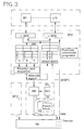
- Physically seen is according to one embodiment a signal data area formed in the system memory SM of the central processor unit which is central or distributed (se particularly Fig. 3).
- the data part is stored in an extension of the register memory RM of the execution processor IPU.
- Fig. 1 are thus the logical relationships illustrated.
- the control information part HEAD is in the buffer memory JBU of the signal processor SPU and the data part BODY logically forms an extension of the buffer memory JBU.
- control information part HEAD is transferred to the register memory RM of the execution processor and the data part then logically forms an extension of the register memory RM.
- the physical location of the data part BODY may either be in the system memory SM or in an extended register memory RM. Pointers are obtained from a free queue list and this must follow the control information part HEAD so that the data belonging to the signal can be reached.
- the control information part HEAD is fetched from the register memory RM and through utilization of the pointer, the signal data is fetched from the signal data area of the system memory SM or alternatively the register memory RM of the execution processor.
- data transports to and from the system memory of central processor system SM or the register memory RM are carried out by a direct memory access DMA which is known per se. The memory accesses may then be stolen, so called cycle stealings, without disturbing memory activities going on parallelly in the job executing processor(s).
- Fig. 3 the system for processing of signal data is described more in detail.
- Signal communication with regional processors RP takes place via interface circuits comprising protocol handlers or so called regional processors handlers i-RPH.
- Such units operate independently handling signals to and from regional processors RP and generally they can handle a number of regional processors.
- the regional processor handlers RPH can access the central buss of the central processor system and they can among others address the memory SM of the central processor themselves.
- other peripheral system units can via an input/output system I/O communicate with protocol handlers i-RPH.
- Incoming signals are thus handled by a signal distributing system which comprises a signal processor or a dedicated processor SPU.
- the signal distributing system includes the above mentioned protocol handlers i-RPH which form interface circuits.
- the interprocessor cooperation itself can for example be carried out essentially in agreement with what is given in SE-B-439 208.
- the regional processors cooperate with each other through an independent stored-program-controlled cooperation signal distribution system.
- requests and message transfer are carried out between different regional processors.
- Incoming cooperation signals from the regional processors are arranged in order of priority or in different priority levels by the signal distribution system. To be able to prioritize in this manner, the function block of the cooperation signal distribution system must be able to understand the incoming messages. If for example different regional processors use different standards, the signal distribution system conveniently adapts an incoming signal to the desired standard, according to an advantageous embodiment to the standard of the called processor.
- function blocks can be arranged for sorting the regional processors into categories which particularly may depend on the current multiprocessor organization. This can be done in any desired manner, for example so that all processors can call each other or that only some of the them can call certain other processors etc. Alternatively can only a central processor receive calls from a regional processor or no regional processors can call each other etc.
- the signal processor SPU communicates, as referred to above, with peripheral processors, for example regional processors RP or similar via interface-protocol handlers i-RPH which are adapted to the interprocessor communication as desired in the system.
- peripheral processors for example regional processors RP or similar
- interface-protocol handlers i-RPH may for example contain intermediate buffers (not shown) for speed adaptation or for adaption between different standards of regional processors and/or central processors.
- intermediate buffers not shown
- the signal processor SPU initiates one or more executing processors IPU 1 , IPU 2 , ... for every signal relating to function block execution.
- Every central processor comprises a number of function blocks each of which has been assigned as specific function).
- all traffic controlling data processing is done with temporary data in internal process registers RM of the job execution processors IPU i .
- temporary data is considered signal data transferred by the signal processor SPU to the process register RM of the executing processor IPU, which data thus are directly accessible for processing.
- the signal processor SPU and thus also the signal distribution system comprises so called job and signal buffers JBU which advantageously comprise so called FIFO-register (first in-first out) which are arranged for the different priority levels A,B,C.
- the incoming signal is supposed to be of the type as described above, namely comprising a control information part HEAD and a data part BODY.
- the control information part HEAD is in the shown example stored together with a stack pointer in a given priority level after the signal data part BODY has been buffered in the signal system memory SM which e.g. may be common within the central processor system.
- the variables of the system are stored in the system memory SM.
- Signal data BODY can here advantageously be stored in an area structure and according to a particular embodiment the system memory SM is equipped with so called direct memory access DMA.
- Buffered signals stored in job buffer blocks JBU are dealt with in the priority and sequential order as given by the job buffers of the signal processors and they are distributed to the appropriate job executing processor IPU 1 .
- signal transmissions are activated by a job executing processor IPU 1 with an instruction but they are carried out by the signal processor SPU.
- the control information part HEAD of the signal is fetched from the buffer memory JBU in the signal processor SPU for execution.
- the data part BODY of the signal is fetched from the system memory SM.
- the data part BODY can be stored in the register memory RM of the execution processor IPU 1 as described in the foregoing.
- the addressing of the data part takes place with using the pointer of the signal which was buffered in job buffer (buffer memory) JBU together with the control information part HEAD as also mentioned above.
- outgoing signal data can be buffered intermediately (not shown here) for, when there is a need, taking internal time differences into account before transmission to peripheral system units or regional processors RP.
- a job execution processor IPU may, in a manner known per se, in addition to a register memory also comprise a data processing unit ALU, and then in a program stores PS store a number of function blocks. It may also comprise so called reference memories (not shown here).
- the system according to the invention may comprise a substantially arbitrary number of regional processors and a number of central processor units wherein every central processor unit comprises at least one signal processor SPU and a job executing processor IPU.
- every central processor unit comprises at least one signal processor SPU and a job executing processor IPU.
- signal processors SPU and a number of job execution processors IPU 1 belonging thereto can be provided.
- the system is applied in a system for telecommunication or for datacommunication.
- the system is particularly used within ISDN-communication (Integrated Services Digital Network).
- the telecommunication system can e.g. be the so called AXE-system (by LM Ericsson) which comprises a switching part and a control part.
- This control part comprises among others a regional processor sub-system and a central processor sub-system and a number input/output systems (I/O).
- the processor comprises a number of function blocks each assigned a specific function.
- the regional processor system and the central processor system respectively particularly comprise a system as disclosed by the present invention.
- the signal format may be according to CCITT (ITU-T) signalling system no. 7 etc. in which case the control information part HEAD for example comprises 16 bytes and the data part for example 256 bytes.
- CCITT ITU-T
- the control information part HEAD for example comprises 16 bytes
- the data part for example 256 bytes.
- any signal format can be used.
Landscapes
- Engineering & Computer Science (AREA)
- Computer Hardware Design (AREA)
- Theoretical Computer Science (AREA)
- Physics & Mathematics (AREA)
- General Engineering & Computer Science (AREA)
- Software Systems (AREA)
- General Physics & Mathematics (AREA)
- Mathematical Physics (AREA)
- Computer Networks & Wireless Communication (AREA)
- Multi Processors (AREA)
Description
- FIG 1
- illustrates an example on logical signal data processing,
- FIG 2
- illustrates an example on a divided signal format and
- FIG 3
- illustrates an example on a system for processing of signal data according to the invention wherein the data part is stored in a system memory.
Claims (21)
- System for signal and data processing comprising a central processor system comprising at least two processors (SPU, IPU), and at least one regional processor (RP) wherein the central processor system comprises a number of function blocks, signal handling to and from for example a regional processor (RP) being handled by a signal handling system (RPH) of the central processor system and wherein one of the processors of the central processor system comprises a signal processor (SPU) which cooperates with one or more of said at least two processors as execution processors (IPUi) through cooperation signals wherein the signal handling between the function blocks is controlled by the signal processor (SPU) through said cooperation signals,
characterized in,
that each signal comprises a control information part (HEAD) and a data part (BODY) and in that for every incoming signal the control information part (HEAD) is stored in a buffer memory (JBU) of the signal processor (SPU) together with a pointer whereas the data part (BODY) is stored in another memory (SM;RM) and in that upon execution the control information part (HEAD) stored in the buffer memory and the pointer are transferred to the register memory (RM) of the execution processor (IPU) whereas the data part (BODY) only is fetched if it is to be processed and in that the data part (BODY) then can be easily accessed for processing in the register memory (RM) of the execution processor (IPU) so that unnecessary transportations of data are avoided. - System according to claim 1,
characterized in,
that the data part (BODY) is stored in a system memory (SM). - System according to claim 1,
characterized in,
that the data part (BODY) is stored in the register memory (RM) of an execution processor (IPU) or in a logical extension thereof. - System according to claim 2 or 3,
characterized in,
that the data part (BODY) of a signal is fetched from the system memory (SM) by the control information part (HEAD) and the stack pointer accompanying the control information part (HEAD) or alternatively from the logical extension of the register memory (RM) if stored therein. - System according to anyone of the preceding claims,
characterized in,
that direct memory access technique (DMA) is used for transporting data to and from the system memory (SM). - System according to anyone of the preceding claims,
characterized in,
that the signal processor (SPU) via interface protocol handlers (i-RPH) communicates with peripheral units or for example regional processors (RP). - System according to claim 6,
characterized in,
that the interface protocol handlers (i-RPH) are provided with an intermediate storage for adapting the speed between the units. - System according to anyone of the preceding claims,
characterized in,
that the signal processor (SPU) initiates an execution processor (IPU) for a signal relating to function block execution. - System according to anyone of claims 1-7,
characterized in,
that the signal processor (SPU) initiates more than one execution processor (IPU) for a function block execution signal. - System according to anyone of the preceding claims,
characterized in,
that signal data being transferred from the signal processor (SPU) to a register memory (RM) of an executing processor (IPU) form temporary data directly accessible for processing. - System according to anyone of the preceding claims,
characterized in,
that the cooperation processor (SPU) comprises job and signal buffers (JBU) which are arranged in priority levels (A,B,C). - System according to claim 11,
characterized in,
that the job and signal buffers comprise FIFO-registers (first in/first out). - System according to claim 12,
characterized in,
that the control information part (HEAD) is stored in a given priority level (A,B,C) after storing of the data part (BODY) in the system memory (SM) or in the register memory (RM) of the execution processor. - System according to anyone of the preceding claims,
characterized in,
that signal transmissions are activated by an execution processor (IPU) with an instruction and in that signal transmissions are carried out by the cooperation processor (SPU). - System according to anyone of the preceding claims,
characterized in,
that output signal data is buffered for adaptation of internal time differences at output to peripheral units. - System according to anyone of the preceding claims,
characterized in,
that it comprises more than one execution processor (IPU1, IPU2). - System according to anyone of the preceding claims,
characterized in,
that it is comprised by a communications system and in that the format of the signals are given by the signalling system 7 (SS 7). - Method for signal and data processing in a control computer system with a central processor system comprising at least two processors (SPU, IPU) and a regional processor system comprising at least one regional processor (RP) wherein the signal processor (SPU) of the central processor system controls the handling of signals between different function blocks comprised by the central processor system via cooperation signals, the signals being divided into a control information part (HEAD) and a data part (BODY),
characterized in,
that each incoming signal is stored as a queue buffer in a buffer memory (JBU) of the signal processor (SPU) in such a way that:the control information part of the signal (HEAD) together with a pointer are stored in the buffer memory (JBU) of the signal processor (SPU),the data part (BODY) of the signal is stored separately in a memory (SM;RM),at execution the control information part (HEAD) and the pointer are transferred to the register memory (RM) of an execution processor (IPU),and in that the data part (BODY) only is fetched when it is to be processed in the register memory (RM) of the execution processor so that unnecessary transportations of data are avoided. - Method according to claim 18,
characterized in,
that the data part (BODY) is stored in a system memory (SM). - Method according to claim 19,
characterized in,
that the data part (BODY) is stored in the register memory (RM) of the execution processor (IPU). - Stored-program-controlled communication system comprising a switching part and a control part, the control part comprising a number of function blocks assigned given functions wherein the system comprises a central processor system as defined in claim 1, an input/output system (I/O) and a regional processor system comprising a number of regional processors (RP) wherein signal processing between the regional processor system and the central processor system is handled by said signal handling system (RPH).
Applications Claiming Priority (3)
| Application Number | Priority Date | Filing Date | Title |
|---|---|---|---|
| SE9403533 | 1994-10-17 | ||
| SE9403533A SE515265C2 (en) | 1994-10-17 | 1994-10-17 | Systems and methods for processing signal data and communication systems comprising a signal data processing system |
| PCT/SE1995/001216 WO1996012235A1 (en) | 1994-10-17 | 1995-10-17 | System and method for processing of signal data and a communication system comprising a signal data processing system |
Publications (2)
| Publication Number | Publication Date |
|---|---|
| EP0791198A1 EP0791198A1 (en) | 1997-08-27 |
| EP0791198B1 true EP0791198B1 (en) | 2001-05-09 |
Family
ID=20395635
Family Applications (1)
| Application Number | Title | Priority Date | Filing Date |
|---|---|---|---|
| EP95935640A Expired - Lifetime EP0791198B1 (en) | 1994-10-17 | 1995-10-17 | System and method for processing of signal data and a communication system comprising a signal data processing system |
Country Status (9)
| Country | Link |
|---|---|
| US (1) | US5951654A (en) |
| EP (1) | EP0791198B1 (en) |
| JP (1) | JPH10507551A (en) |
| KR (1) | KR100291301B1 (en) |
| CN (1) | CN1097785C (en) |
| CA (1) | CA2202862A1 (en) |
| DE (1) | DE69520886T2 (en) |
| SE (1) | SE515265C2 (en) |
| WO (1) | WO1996012235A1 (en) |
Families Citing this family (28)
| Publication number | Priority date | Publication date | Assignee | Title |
|---|---|---|---|---|
| SE515265C2 (en) * | 1994-10-17 | 2001-07-09 | Ericsson Telefon Ab L M | Systems and methods for processing signal data and communication systems comprising a signal data processing system |
| US6154460A (en) * | 1997-05-30 | 2000-11-28 | Alcatel Usa Sourcing, L.P. | Data packet transmission system and method |
| US6366663B1 (en) | 1997-07-21 | 2002-04-02 | Mci Communications Corporation | System for achieving local number portability |
| US6157968A (en) * | 1998-01-26 | 2000-12-05 | Motorola Inc. | Interface with selector receiving control words comprising device identifiers for determining corresponding communications parameter set for interface port transfer of data words to peripheral devices |
| JPH11232040A (en) * | 1998-02-17 | 1999-08-27 | Sony Corp | Data output device and method |
| US8044793B2 (en) | 2001-03-01 | 2011-10-25 | Fisher-Rosemount Systems, Inc. | Integrated device alerts in a process control system |
| US7562135B2 (en) | 2000-05-23 | 2009-07-14 | Fisher-Rosemount Systems, Inc. | Enhanced fieldbus device alerts in a process control system |
| US7206646B2 (en) | 1999-02-22 | 2007-04-17 | Fisher-Rosemount Systems, Inc. | Method and apparatus for performing a function in a plant using process performance monitoring with process equipment monitoring and control |
| US6473503B1 (en) | 1999-08-31 | 2002-10-29 | Worldcom, Inc. | System, method and computer program product for achieving local number portability network management support |
| US6438219B1 (en) | 1999-08-31 | 2002-08-20 | Worldcom, Inc. | System, method and computer program product for achieving local number portability costing support |
| US6473502B1 (en) | 1999-08-31 | 2002-10-29 | Worldcom, Inc. | System, method and computer program product for achieving local number portability costing and network management support |
| JP2004533036A (en) | 2001-03-01 | 2004-10-28 | フィッシャー−ローズマウント システムズ, インコーポレイテッド | Data sharing in process plants |
| US7720727B2 (en) | 2001-03-01 | 2010-05-18 | Fisher-Rosemount Systems, Inc. | Economic calculations in process control system |
| JP4160399B2 (en) | 2001-03-01 | 2008-10-01 | フィッシャー−ローズマウント システムズ, インコーポレイテッド | Creating and displaying indicators in the process plant |
| US8073967B2 (en) * | 2002-04-15 | 2011-12-06 | Fisher-Rosemount Systems, Inc. | Web services-based communications for use with process control systems |
| CN1295633C (en) * | 2002-12-26 | 2007-01-17 | 华为技术有限公司 | Method for multiple CPU communication |
| CN100347674C (en) * | 2004-06-09 | 2007-11-07 | 宏正自动科技股份有限公司 | Intelligent platform management interface system and execution method thereof |
| US9201420B2 (en) | 2005-04-08 | 2015-12-01 | Rosemount, Inc. | Method and apparatus for performing a function in a process plant using monitoring data with criticality evaluation data |
| US8005647B2 (en) | 2005-04-08 | 2011-08-23 | Rosemount, Inc. | Method and apparatus for monitoring and performing corrective measures in a process plant using monitoring data with corrective measures data |
| US7272531B2 (en) | 2005-09-20 | 2007-09-18 | Fisher-Rosemount Systems, Inc. | Aggregation of asset use indices within a process plant |
| BRPI0722378A2 (en) | 2006-03-31 | 2012-05-22 | Qualcomm Incorporated | high speed media access memory management |
| US8301676B2 (en) | 2007-08-23 | 2012-10-30 | Fisher-Rosemount Systems, Inc. | Field device with capability of calculating digital filter coefficients |
| US7702401B2 (en) | 2007-09-05 | 2010-04-20 | Fisher-Rosemount Systems, Inc. | System for preserving and displaying process control data associated with an abnormal situation |
| US8055479B2 (en) | 2007-10-10 | 2011-11-08 | Fisher-Rosemount Systems, Inc. | Simplified algorithm for abnormal situation prevention in load following applications including plugged line diagnostics in a dynamic process |
| CN101930353A (en) * | 2009-06-25 | 2010-12-29 | 龙迅半导体科技(合肥)有限公司 | Implementation of MCS551 serial MCU (Microprogrammed Control Unit) double data pointer |
| US9927788B2 (en) | 2011-05-19 | 2018-03-27 | Fisher-Rosemount Systems, Inc. | Software lockout coordination between a process control system and an asset management system |
| US9342362B2 (en) * | 2012-06-15 | 2016-05-17 | Nvidia Corporation | Service-processor-centric computer architecture and method of operation thereof |
| CN117130977A (en) * | 2023-08-17 | 2023-11-28 | 沈阳航盛科技有限责任公司 | A fiber optic board for large data volume communication based on hardware cache |
Family Cites Families (6)
| Publication number | Priority date | Publication date | Assignee | Title |
|---|---|---|---|---|
| SE439208B (en) * | 1983-09-30 | 1985-06-03 | Ericsson Telefon Ab L M | PROGRAMMED CONTROL TELECOMMUNICATIONS |
| US4601586A (en) * | 1984-02-10 | 1986-07-22 | Prime Computer, Inc. | Solicited message packet transfer system |
| US4755986A (en) * | 1985-09-13 | 1988-07-05 | Nec Corporation | Packet switching system |
| US5315707A (en) * | 1992-01-10 | 1994-05-24 | Digital Equipment Corporation | Multiprocessor buffer system |
| SE515265C2 (en) * | 1994-10-17 | 2001-07-09 | Ericsson Telefon Ab L M | Systems and methods for processing signal data and communication systems comprising a signal data processing system |
| US5870394A (en) * | 1996-07-23 | 1999-02-09 | Northern Telecom Limited | Method and apparatus for reassembly of data packets into messages in an asynchronous transfer mode communications system |
-
1994
- 1994-10-17 SE SE9403533A patent/SE515265C2/en not_active IP Right Cessation
-
1995
- 1995-10-17 JP JP8513167A patent/JPH10507551A/en active Pending
- 1995-10-17 US US08/817,511 patent/US5951654A/en not_active Expired - Lifetime
- 1995-10-17 EP EP95935640A patent/EP0791198B1/en not_active Expired - Lifetime
- 1995-10-17 WO PCT/SE1995/001216 patent/WO1996012235A1/en not_active Ceased
- 1995-10-17 CA CA002202862A patent/CA2202862A1/en not_active Abandoned
- 1995-10-17 DE DE69520886T patent/DE69520886T2/en not_active Expired - Lifetime
- 1995-10-17 CN CN95196647A patent/CN1097785C/en not_active Expired - Fee Related
- 1995-10-17 KR KR1019970702472A patent/KR100291301B1/en not_active Expired - Fee Related
Also Published As
| Publication number | Publication date |
|---|---|
| SE9403533L (en) | 1996-04-18 |
| CA2202862A1 (en) | 1996-04-25 |
| SE515265C2 (en) | 2001-07-09 |
| DE69520886T2 (en) | 2001-11-29 |
| US5951654A (en) | 1999-09-14 |
| EP0791198A1 (en) | 1997-08-27 |
| CN1097785C (en) | 2003-01-01 |
| WO1996012235A1 (en) | 1996-04-25 |
| KR100291301B1 (en) | 2001-06-01 |
| SE9403533D0 (en) | 1994-10-17 |
| DE69520886D1 (en) | 2001-06-13 |
| CN1168731A (en) | 1997-12-24 |
| JPH10507551A (en) | 1998-07-21 |
Similar Documents
| Publication | Publication Date | Title |
|---|---|---|
| US5951654A (en) | System for processing cooperation signals by storing and executing the control part of the signal separately from the data part using pointer to link the two parts | |
| US4543627A (en) | Internal communication arrangement for a multiprocessor system | |
| US5418781A (en) | Architecture for maintaining the sequence of packet cells transmitted over a multicast, cell-switched network | |
| CA1055162A (en) | Arrangement for switching of data | |
| KR100379342B1 (en) | Intelligent memory-based input/output system | |
| EP1399817B1 (en) | Methods and apparatus for regulating process state control messages | |
| US4918597A (en) | Adaptive interface for transferring segmented message between device and microcomputer on line division multiplexed bus | |
| JPS5897944A (en) | Data transfer system among microprocessors | |
| US5408468A (en) | Queueing system for switches having fast circuit properties | |
| US20060209827A1 (en) | Systems and methods for implementing counters in a network processor with cost effective memory | |
| US6032174A (en) | Load sharing system and a method for processing of data and a communication system with load sharing | |
| JPS6298842A (en) | Packet switching system | |
| KR950003680B1 (en) | Message Queue Management Method for Common Line Signaling in Electronic Switching System | |
| US5925121A (en) | Data processing system and method for accessing a common data memory | |
| JPH02288760A (en) | Incoming call control system in multi-processor controlled electronic exchange | |
| KR100293363B1 (en) | Transmission queue management method of communication control board between processors of all electronic exchange | |
| JPH07123311B2 (en) | Subscriber data management method | |
| KR20000028318A (en) | Method for treating message using common buffer in atm switching system | |
| Brofferio et al. | Electronic Distributed Switching Systems (EDSS): A distributed structure for the coordinating processor | |
| JPS63262746A (en) | Synchronizing system for common data in multi-processor system | |
| Rowan et al. | Toward the design of a network manager for a distributed computer network | |
| JPH02149095A (en) | Multiprocessor type accumulation program controlling exchange system | |
| JPH04276946A (en) | Decentralized system for inter-network protocol control section | |
| KR19990061239A (en) | Apparatus and method for processing signaling protocol in asynchronous transfer mode exchange | |
| JPH0250598A (en) | Signal distributing method for electronic exchange |
Legal Events
| Date | Code | Title | Description |
|---|---|---|---|
| PUAI | Public reference made under article 153(3) epc to a published international application that has entered the european phase |
Free format text: ORIGINAL CODE: 0009012 |
|
| 17P | Request for examination filed |
Effective date: 19970506 |
|
| AK | Designated contracting states |
Kind code of ref document: A1 Designated state(s): DE FR GB NL |
|
| GRAG | Despatch of communication of intention to grant |
Free format text: ORIGINAL CODE: EPIDOS AGRA |
|
| 17Q | First examination report despatched |
Effective date: 20000829 |
|
| GRAG | Despatch of communication of intention to grant |
Free format text: ORIGINAL CODE: EPIDOS AGRA |
|
| GRAH | Despatch of communication of intention to grant a patent |
Free format text: ORIGINAL CODE: EPIDOS IGRA |
|
| GRAH | Despatch of communication of intention to grant a patent |
Free format text: ORIGINAL CODE: EPIDOS IGRA |
|
| GRAA | (expected) grant |
Free format text: ORIGINAL CODE: 0009210 |
|
| AK | Designated contracting states |
Kind code of ref document: B1 Designated state(s): DE FR GB NL |
|
| PG25 | Lapsed in a contracting state [announced via postgrant information from national office to epo] |
Ref country code: NL Free format text: LAPSE BECAUSE OF FAILURE TO SUBMIT A TRANSLATION OF THE DESCRIPTION OR TO PAY THE FEE WITHIN THE PRESCRIBED TIME-LIMIT Effective date: 20010509 |
|
| REF | Corresponds to: |
Ref document number: 69520886 Country of ref document: DE Date of ref document: 20010613 |
|
| ET | Fr: translation filed | ||
| NLV1 | Nl: lapsed or annulled due to failure to fulfill the requirements of art. 29p and 29m of the patents act | ||
| REG | Reference to a national code |
Ref country code: GB Ref legal event code: IF02 |
|
| PLBE | No opposition filed within time limit |
Free format text: ORIGINAL CODE: 0009261 |
|
| STAA | Information on the status of an ep patent application or granted ep patent |
Free format text: STATUS: NO OPPOSITION FILED WITHIN TIME LIMIT |
|
| 26N | No opposition filed | ||
| PGFP | Annual fee paid to national office [announced via postgrant information from national office to epo] |
Ref country code: FR Payment date: 20121107 Year of fee payment: 18 Ref country code: DE Payment date: 20121029 Year of fee payment: 18 |
|
| PGFP | Annual fee paid to national office [announced via postgrant information from national office to epo] |
Ref country code: GB Payment date: 20121025 Year of fee payment: 18 |
|
| GBPC | Gb: european patent ceased through non-payment of renewal fee |
Effective date: 20131017 |
|
| PG25 | Lapsed in a contracting state [announced via postgrant information from national office to epo] |
Ref country code: GB Free format text: LAPSE BECAUSE OF NON-PAYMENT OF DUE FEES Effective date: 20131017 |
|
| REG | Reference to a national code |
Ref country code: DE Ref legal event code: R119 Ref document number: 69520886 Country of ref document: DE Effective date: 20140501 |
|
| REG | Reference to a national code |
Ref country code: FR Ref legal event code: ST Effective date: 20140630 |
|
| PG25 | Lapsed in a contracting state [announced via postgrant information from national office to epo] |
Ref country code: DE Free format text: LAPSE BECAUSE OF NON-PAYMENT OF DUE FEES Effective date: 20140501 Ref country code: FR Free format text: LAPSE BECAUSE OF NON-PAYMENT OF DUE FEES Effective date: 20131031 |