EP0790633A2 - Electron source and electron beam-emitting apparatus equipped therewith - Google Patents
Electron source and electron beam-emitting apparatus equipped therewith Download PDFInfo
- Publication number
- EP0790633A2 EP0790633A2 EP97101980A EP97101980A EP0790633A2 EP 0790633 A2 EP0790633 A2 EP 0790633A2 EP 97101980 A EP97101980 A EP 97101980A EP 97101980 A EP97101980 A EP 97101980A EP 0790633 A2 EP0790633 A2 EP 0790633A2
- Authority
- EP
- European Patent Office
- Prior art keywords
- electron
- needle
- tip
- electron beam
- voltage
- Prior art date
- Legal status (The legal status is an assumption and is not a legal conclusion. Google has not performed a legal analysis and makes no representation as to the accuracy of the status listed.)
- Granted
Links
- 238000000605 extraction Methods 0.000 claims abstract description 39
- 238000010894 electron beam technology Methods 0.000 claims abstract description 20
- 230000005684 electric field Effects 0.000 claims description 3
- 239000000523 sample Substances 0.000 abstract description 16
- 238000000609 electron-beam lithography Methods 0.000 abstract description 4
- 230000007423 decrease Effects 0.000 abstract description 3
- 239000013078 crystal Substances 0.000 description 18
- 230000003287 optical effect Effects 0.000 description 5
- 238000009792 diffusion process Methods 0.000 description 4
- 238000002474 experimental method Methods 0.000 description 3
- 238000000034 method Methods 0.000 description 3
- 238000011109 contamination Methods 0.000 description 2
- 229910052760 oxygen Inorganic materials 0.000 description 2
- 238000001878 scanning electron micrograph Methods 0.000 description 2
- 238000001179 sorption measurement Methods 0.000 description 2
- 229910052726 zirconium Inorganic materials 0.000 description 2
- MYMOFIZGZYHOMD-UHFFFAOYSA-N Dioxygen Chemical compound O=O MYMOFIZGZYHOMD-UHFFFAOYSA-N 0.000 description 1
- 229910025794 LaB6 Inorganic materials 0.000 description 1
- ZOKXTWBITQBERF-UHFFFAOYSA-N Molybdenum Chemical compound [Mo] ZOKXTWBITQBERF-UHFFFAOYSA-N 0.000 description 1
- 230000004913 activation Effects 0.000 description 1
- 238000010420 art technique Methods 0.000 description 1
- QVGXLLKOCUKJST-UHFFFAOYSA-N atomic oxygen Chemical compound [O] QVGXLLKOCUKJST-UHFFFAOYSA-N 0.000 description 1
- 230000005540 biological transmission Effects 0.000 description 1
- 230000015572 biosynthetic process Effects 0.000 description 1
- 239000000919 ceramic Substances 0.000 description 1
- 238000010276 construction Methods 0.000 description 1
- 238000010586 diagram Methods 0.000 description 1
- 229910001882 dioxygen Inorganic materials 0.000 description 1
- 230000000694 effects Effects 0.000 description 1
- 238000005516 engineering process Methods 0.000 description 1
- 229910052735 hafnium Inorganic materials 0.000 description 1
- 239000001257 hydrogen Substances 0.000 description 1
- 229910052739 hydrogen Inorganic materials 0.000 description 1
- -1 hydrogen compound Chemical class 0.000 description 1
- 230000001939 inductive effect Effects 0.000 description 1
- 239000012212 insulator Substances 0.000 description 1
- 239000000463 material Substances 0.000 description 1
- 238000005259 measurement Methods 0.000 description 1
- 229910052751 metal Inorganic materials 0.000 description 1
- 239000002184 metal Substances 0.000 description 1
- 229910052750 molybdenum Inorganic materials 0.000 description 1
- 239000011733 molybdenum Substances 0.000 description 1
- 239000001301 oxygen Substances 0.000 description 1
- 125000004430 oxygen atom Chemical group O* 0.000 description 1
- 238000005498 polishing Methods 0.000 description 1
- 239000003870 refractory metal Substances 0.000 description 1
- 230000000717 retained effect Effects 0.000 description 1
- 239000004065 semiconductor Substances 0.000 description 1
- 229910001220 stainless steel Inorganic materials 0.000 description 1
- 239000010935 stainless steel Substances 0.000 description 1
- 229910052719 titanium Inorganic materials 0.000 description 1
- WFKWXMTUELFFGS-UHFFFAOYSA-N tungsten Chemical compound [W] WFKWXMTUELFFGS-UHFFFAOYSA-N 0.000 description 1
- 229910052721 tungsten Inorganic materials 0.000 description 1
- 239000010937 tungsten Substances 0.000 description 1
Images

Classifications
-
- H—ELECTRICITY
- H01—ELECTRIC ELEMENTS
- H01J—ELECTRIC DISCHARGE TUBES OR DISCHARGE LAMPS
- H01J37/00—Discharge tubes with provision for introducing objects or material to be exposed to the discharge, e.g. for the purpose of examination or processing thereof
- H01J37/02—Details
- H01J37/04—Arrangements of electrodes and associated parts for generating or controlling the discharge, e.g. electron-optical arrangement or ion-optical arrangement
- H01J37/06—Electron sources; Electron guns
-
- H—ELECTRICITY
- H01—ELECTRIC ELEMENTS
- H01J—ELECTRIC DISCHARGE TUBES OR DISCHARGE LAMPS
- H01J2237/00—Discharge tubes exposing object to beam, e.g. for analysis treatment, etching, imaging
- H01J2237/06—Sources
- H01J2237/063—Electron sources
- H01J2237/06308—Thermionic sources
- H01J2237/06316—Schottky emission
Definitions
- the present invention relates to an electron source used in practical apparatus using an electron beam such as an electron microscope or electron beam lithography machine.
- a surface diffusion type electron source has been put into practical use as a new electron source.
- This source is fabricated by adsorbing monatomic layers of Zr, Ti, Hf, or the like and of oxygen atoms onto the surface of a single-crystal tip of a refractory metal material such as tungsten (W) or molybdenum (Mo).
- a refractory metal material such as tungsten (W) or molybdenum (Mo).
- W tungsten
- Mo molybdenum
- a powdered hydrogen compound such as hydrogenated Zr is made to adhere between the W hairpin filament and the single-crystal needle and heat-treated in a vacuum ambient having a partial pressure of oxygen gas to promote diffusion of Zr or the like. In this way, adsorption layers of Zr and O are formed in the given crystallographic crystal plane at the tip of the single crystal (U.S. Pat. No. 4,324,999).
- this electron source is used in a weak field region where no field emission takes place, it is referred to as Schottky emission.
- Zr/O/W has been put into practical use as this electron source ( J. of Vac. Sci. Technol . B3 (1), 1985, p. 220)).
- a control electrode (generally referred to as a suppressor electrode) and an extraction electrode are added to this electron source, thus constituting an electron gun.
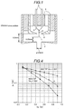
- the fundamental structure of this gun is shown in Fig. 1. Shown in this figure are a single-crystal needle of W (100), indicated by 1, a hairpin filament 2 of polycrystalline W, a terminal 4 of stainless steel or the like to which the filament 2 is spot-welded, and a ceramic insulator 5.
- An oxide source 3 of Z having a lower work function than the single-crystal needle 1 of W is attached either to the center or base of the single-crystal needle 1 or to the filament 2. This oxide source 3 is heated to about 1500 K to 1900 K to induce thermal diffusion along the single-crystal needle 1 up to its tip.
- the metal (Zr) oxide diffused to the tip of the single-crystal needle 1 forms a Zr monatomic layer, together with oxygen, at the tip of the single-crystal needle 1.
- the layer is preferentially formed by adsorption onto the surface where the surface diffusion has occurred and also onto the certain crystal plane (100) having a higher activation energy. If such a single-crystal needle is used that the (100) crystal plane forms the tip of the single-crystal needle 1, then only the axial end of the single-crystal needle 1 can be left with a low work function. Consequently, a high electron emission current density can be obtained at this location.
- a suppressor electrode 6 acts to suppress thermoelectrons from the W hairpin filament heated to 1500 K to 1900 K.
- An extraction electrode 7 serves to cause Schottky emission (hereinafter abbreviated SE) by applying an electric field to the tip of the single crystal.
- SE Schottky emission
- the field intensity applied to the tip by the SE is much lower than in field emission. Accordingly, emitted electrons are thermoelectrons and do not contain tunnel electrons. This means that variations in the emission electron stream intrinsic to field emission electrons do not take place. Hence, a quite stable emission electron stream is obtained.
- the operating temperature is lower than that of a normal thermionic source such as LaB6 or W hairpin and so the energy spread of the emitted electron stream can be narrowed.
- the amount of electron beam emitted from the above-described SE electron source depends on the field intensity at the tip of the needle as described in the above-cited literature. Therefore, it is common practice to adjust the electron beam amount by the extraction voltage applied to the extraction electrode.
- the gap between the control electrode and the needle tip and the gap between the control electrode and the extraction electrode are quite small, as can be seen from Fig. 1. Therefore, it is desired to reduce the values of voltages applied to these electrodes.
- the electron beam amount can be adjusted only within a narrow range.
- the voltages applied to the electrodes are high and so electric discharge tends to occur easily. This can cause a damage to the needle tip.
- an electron source comprising a needlelike cathode having a tip formed by a cone angle of less than 15 degrees, a control electrode for controlling the amount of electron beam from the cathode, and an extraction electrode for extracting electrons from the needlelike cathode.
- the inventive configuration also discloses an electron beam-emitting apparatus which varies the negative voltage value applied to the control voltage while maintaining constant the positive voltage applied to the extraction electrode, thus varying the amount of electron beam.
- the tip of the cathode is so shaped that it has a radius of curvature of less than 0.5 ⁇ m.
- the optical axis is varied to a lesser extent and greater advantages are obtained by adjusting the control voltage applied to the control electrode than by adjusting the electron beam amount by means of the extraction voltage. That is, ideally, every used electron beam amount can be adjusted by varying the control voltage under a given extraction voltage setting.
- the field intensity at the tip of the SE needle depends on the structure of the electron source itself.
- Fig. 2 shows SEM images of the tips of two kinds of needles used in the present embodiment.
- the magnification is 10,000 xfor both images.
- Fig. 2(a) shows the conventional needle having a cone angle (2 ⁇ ) of 26 degrees and a radius of curvature ( r ) of 0.55 ⁇ m.
- Fig. 2(b) is an SEM image of the tip of the novel needle. This has a cone angle (2 ⁇ ) of 8 degrees and a radius of curvature ( r ) of 0.30 ⁇ m.
- the field intensity can be increased by making both parameters as small as possible. In this way, a large field intensity can be created even under a small extraction voltage.
- the above-cited literature makes no mention of the effect of the control voltage.
- Our experiment has revealed that the electric field created by the control voltage applied to the control electrode increases by reducing the two parameters.
- the variation in the field intensity at the tip of the needle per unit voltage variation can be made larger than heretofore.
- the present invention can provide an electron source capable of covering the whole range of usable electron beam amounts at one extraction voltage setting by adjusting the control voltage, as well as an electron beam lithography machine equipped with this electron source.
- the emission current density depends on the temperature T of the needle, on the work function ⁇ of the emitting surface, and on the field intensity F at the tip of the needle.
- This field intensity F depends on the cone angle of the tip itself and on the radius of curvature.
- the field intensity F also depends on the space between the SE needle and the extraction electrode. As shown in Fig. 1, the space between the SE needle and the extraction electrode is quite small and so it is difficult to adjust the space further. Therefore, the range of variations in field intensity at the tip of the needle which are caused when the control voltage is varied in a desired range can be enlarged by carrying out adjustment of the cone angle and of the radius of curvature.
- the present invention provides a novel combination of a Schottky emission electron source sharpened to less than 15 degrees and a method of controlling the amount of electron beam by means of control voltages applied to the control electrode. This increases the range of probe currents obtained in response to variations in control voltage. As a result, the kinds of the voltages applied to the extraction voltage can be reduced to a minimum.
- the ideal method is to secure a desired probe current range with a single extraction voltage setting. This is based on the premise that the optical axis or the position of the virtual light source is not varied by variations in control electrode.
- the range of variations in electron beam amount emitted from the electron source can be increased for a given variation in control voltage, by adjusting the cone angle and radius of curvature and also adjusting the amount of the electron beam by means of the control electrode.
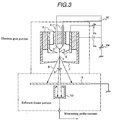
- Fig. 3 is a testing machine evacuated to an ultrahigh vacuum and used to evaluate SE electron guns. It is composed of an electron gun portion and an evacuated frame portion. The machine evaluates the characteristics of numerous guns by replacing the electron gun portion. First, the electron gun portion on which an SE needle is installed is placed on the evacuated frame portion and evacuated to an ultrahigh vacuum. Then, a hairpin filament is electrically energized from a constant current source Vf to heat it. The temperature of the SE needle is maintained at a desired constant temperature between 1600 K and 1800 K.
- a positive voltage is applied to the extraction electrode from a high dc voltage source Ve, thus emitting SE electrons from the tip of the SE needle.
- a negative voltage is applied to the control electrode, or suppressor electrode, from a dc voltage source Vs. This prevents the electrons from leaving the electron path.
- the energy is determined by the high dc voltage source Va.
- a low accelerating voltage of about less than 1 kV is used.
- the SE electrons incident on the Faraday cup form a probe current, which is actually used in an electron microscope or other instrument utilizing an electron beam.
- the aperture angle is of the order of several mrad.
- a current of several pA to several hundreds of pA is obtained.
- the extraction voltage Ve applied to the extraction electrode is kept constant.
- the control voltage is varied over a certain range. The resulting probe current is measured.
- the electron beam amount is controlled according to the value of the negative voltage applied to the control voltage. This makes it unnecessary to control the electron beam amount by the extraction voltage. Since the extraction voltage can be fixed, the electron beam amount can be easily set without inducing axial misalignment.
- control voltage is varied while maintaining the extraction voltage constant.
- the results are shown in Fig. 4.
- the control voltage was varied over a range from 100 V to 900 V. It can be seen from Fig. 4 that with the prior art, or old, needle tip, the probe current varied from 22 pA to 57 pA and that with the novel, or new, needle tip, the current changed over a quite wide range from 2.3 pA to 67 pA.
- the extraction voltage Ve was 1.5 kV, which was smaller than in the case of the prior art needle tip.
- the extraction voltage can be reduced by adopting the novel electron gun. Furthermore, the range in which the probe current varies in response to a given variation in control voltage increases. In this manner, for a given variation in control electrode, the range of variations of the probe current depends on the cone angle and also on the radius of curvature.
- the electron source is built at a cone angle less than this, then it is possible to accommodate the probe current range to the above-described conditions.
- a sophisticated technique is required to sharpen the tip. With today's formation technology, the tip can be sharpened only up to 5-6 degrees.
- the radius of curvature of the tip With respect to the radius of curvature of the tip, if it is set larger than 0.5 ⁇ m, it is difficult to induce Schottky emission and thus the aforementioned beam current range cannot be obtained. If the radius of curvature is set less than 0.2 ⁇ m, field emission makes the beam unstable.
- the above embodiment is implemented in an SE electron source.
- similar advantages are derived from an electron gun in which the probe current is varied by a control voltage, in the same way as the foregoing.
- the invention can be applied to TFE electron source, CFE electron source, and so on, using control electrodes.
- the present invention is generally applicable to every apparatus incorporating such an electron source.
- the invention can be applied with similar utility to scanning electron microscope, transmission electron microscope, electron beam lithography system, and so on.
- the obtained range of probe currents increases for a given variation in control voltage Therefore, the electron beam amount can be set over a wide range with one extraction voltage setting. In consequence, the required range of probe currents can be obtained without varying the extraction voltage. Since the extraction voltage can be retained constant, axial misalignment due to variations of the extraction voltage can be prevented. Additionally, the value of the extraction voltage itself decreases. Therefore, electric discharge is prevented; otherwise the needle would be damaged. This adds to the stability of the electron gun.
Landscapes
- Chemical & Material Sciences (AREA)
- Analytical Chemistry (AREA)
- Electron Sources, Ion Sources (AREA)
- Electron Beam Exposure (AREA)
Abstract
Description
- The present invention relates to an electron source used in practical apparatus using an electron beam such as an electron microscope or electron beam lithography machine.
- In recent years, a surface diffusion type electron source has been put into practical use as a new electron source. This source is fabricated by adsorbing monatomic layers of Zr, Ti, Hf, or the like and of oxygen atoms onto the surface of a single-crystal tip of a refractory metal material such as tungsten (W) or molybdenum (Mo). Generally, this new electron source is constructed in the manner described now. A W single-crystal needle having a given crystallographic orientation is joined to the top of a W hairpin filament. The tip of this single-crystal needle is sharpened by electrolytic polishing. A powdered hydrogen compound such as hydrogenated Zr is made to adhere between the W hairpin filament and the single-crystal needle and heat-treated in a vacuum ambient having a partial pressure of oxygen gas to promote diffusion of Zr or the like. In this way, adsorption layers of Zr and O are formed in the given crystallographic crystal plane at the tip of the single crystal (U.S. Pat. No. 4,324,999). Where this electron source is used in a weak field region where no field emission takes place, it is referred to as Schottky emission. Zr/O/W has been put into practical use as this electron source (J. of Vac. Sci. Technol. B3 (1), 1985, p. 220)). A control electrode (generally referred to as a suppressor electrode) and an extraction electrode are added to this electron source, thus constituting an electron gun. The fundamental structure of this gun is shown in Fig. 1. Shown in this figure are a single-crystal needle of W (100), indicated by 1, a
hairpin filament 2 of polycrystalline W, aterminal 4 of stainless steel or the like to which thefilament 2 is spot-welded, and aceramic insulator 5. An oxide source 3 of Z having a lower work function than the single-crystal needle 1 of W is attached either to the center or base of the single-crystal needle 1 or to thefilament 2. This oxide source 3 is heated to about 1500 K to 1900 K to induce thermal diffusion along the single-crystal needle 1 up to its tip. The metal (Zr) oxide diffused to the tip of the single-crystal needle 1 forms a Zr monatomic layer, together with oxygen, at the tip of the single-crystal needle 1. At this time, the layer is preferentially formed by adsorption onto the surface where the surface diffusion has occurred and also onto the certain crystal plane (100) having a higher activation energy. If such a single-crystal needle is used that the (100) crystal plane forms the tip of the single-crystal needle 1, then only the axial end of the single-crystal needle 1 can be left with a low work function. Consequently, a high electron emission current density can be obtained at this location. Asuppressor electrode 6 acts to suppress thermoelectrons from the W hairpin filament heated to 1500 K to 1900 K. Anextraction electrode 7 serves to cause Schottky emission (hereinafter abbreviated SE) by applying an electric field to the tip of the single crystal. The field intensity applied to the tip by the SE is much lower than in field emission. Accordingly, emitted electrons are thermoelectrons and do not contain tunnel electrons. This means that variations in the emission electron stream intrinsic to field emission electrons do not take place. Hence, a quite stable emission electron stream is obtained. Furthermore, the operating temperature is lower than that of a normal thermionic source such as LaB6 or W hairpin and so the energy spread of the emitted electron stream can be narrowed. - The amount of electron beam emitted from the above-described SE electron source depends on the field intensity at the tip of the needle as described in the above-cited literature. Therefore, it is common practice to adjust the electron beam amount by the extraction voltage applied to the extraction electrode.
- However, whenever the extraction electrode is varied, problems such as optical axis misalignment occur.
- The gap between the control electrode and the needle tip and the gap between the control electrode and the extraction electrode are quite small, as can be seen from Fig. 1. Therefore, it is desired to reduce the values of voltages applied to these electrodes. However, with the prior art electron gun structure, the electron beam amount can be adjusted only within a narrow range. Furthermore, the voltages applied to the electrodes are high and so electric discharge tends to occur easily. This can cause a damage to the needle tip.
- It is an object of the present invention to provide an electron source capable of solving the foregoing problems, as well as an electron beam-emitting apparatus using this electron source.
- In order to achieve the above-described object, the present invention discloses an electron source comprising a needlelike cathode having a tip formed by a cone angle of less than 15 degrees, a control electrode for controlling the amount of electron beam from the cathode, and an extraction electrode for extracting electrons from the needlelike cathode.
- The inventive configuration also discloses an electron beam-emitting apparatus which varies the negative voltage value applied to the control voltage while maintaining constant the positive voltage applied to the extraction electrode, thus varying the amount of electron beam.
- The tip of the cathode is so shaped that it has a radius of curvature of less than 0.5 µm.
- This construction is adopted for the following reasons.
- The optical axis is varied to a lesser extent and greater advantages are obtained by adjusting the control voltage applied to the control electrode than by adjusting the electron beam amount by means of the extraction voltage. That is, ideally, every used electron beam amount can be adjusted by varying the control voltage under a given extraction voltage setting.
- The field intensity at the tip of the SE needle depends on the structure of the electron source itself.
- As described in J. Appl. Phys., Vol. 44, No. 5, 1973, two parameters, i.e., cone angle (2β) and radius of curvature r, affect the field intensity.
- Fig. 2 shows SEM images of the tips of two kinds of needles used in the present embodiment. The magnification is 10,000 xfor both images. Fig. 2(a) shows the conventional needle having a cone angle (2β) of 26 degrees and a radius of curvature (r) of 0.55 µm. Fig. 2(b) is an SEM image of the tip of the novel needle. This has a cone angle (2β) of 8 degrees and a radius of curvature (r) of 0.30 µm. According to the above-cited literature, the field intensity can be increased by making both parameters as small as possible. In this way, a large field intensity can be created even under a small extraction voltage. However, the above-cited literature makes no mention of the effect of the control voltage. Our experiment has revealed that the electric field created by the control voltage applied to the control electrode increases by reducing the two parameters.
- Therefore, in the above structure, the variation in the field intensity at the tip of the needle per unit voltage variation can be made larger than heretofore.
- The present invention can provide an electron source capable of covering the whole range of usable electron beam amounts at one extraction voltage setting by adjusting the control voltage, as well as an electron beam lithography machine equipped with this electron source.
- The current density J emitted from the SE electron source is given by the following equation, in which T is the needle temperature, φ is the work function, a is a constant, F is the field intensity, and k is a constant.

- As can be seen from the above equation, the emission current density depends on the temperature T of the needle, on the work function ø of the emitting surface, and on the field intensity F at the tip of the needle. This field intensity F depends on the cone angle of the tip itself and on the radius of curvature. The field intensity F also depends on the space between the SE needle and the extraction electrode. As shown in Fig. 1, the space between the SE needle and the extraction electrode is quite small and so it is difficult to adjust the space further. Therefore, the range of variations in field intensity at the tip of the needle which are caused when the control voltage is varied in a desired range can be enlarged by carrying out adjustment of the cone angle and of the radius of curvature.
- It has been known that emission of an electron beam is facilitated simply by sharpening the tip. The present invention provides a novel combination of a Schottky emission electron source sharpened to less than 15 degrees and a method of controlling the amount of electron beam by means of control voltages applied to the control electrode. This increases the range of probe currents obtained in response to variations in control voltage. As a result, the kinds of the voltages applied to the extraction voltage can be reduced to a minimum.
- If a desired voltage adjustment range cannot be obtained within the adjustable range of the control electrode, then it is necessary to secure a desired adjustable range of probe currents by adjusting the extraction voltage. However, where the extraction voltage is varied, other parameters must be adjusted with labor. Also, optical axis misalignment occurs. Where these and other drawbacks are taken into account, the ideal method is to secure a desired probe current range with a single extraction voltage setting. This is based on the premise that the optical axis or the position of the virtual light source is not varied by variations in control electrode.
- As described thus far, the range of variations in electron beam amount emitted from the electron source can be increased for a given variation in control voltage, by adjusting the cone angle and radius of curvature and also adjusting the amount of the electron beam by means of the control electrode.
-
- Fig. 1 is a schematic of an SE electron source;
- Fig. 2 shows electron micrograms of cathodes fabricated according to the invention and by the prior art techniques, respectively;
- Fig. 3 is a diagram showing a testing machine for novel needle tips and the prior art needle tips; and
- Fig. 4 is a graph comparing the novel needle tips with the prior art needle tips.
- Embodiments of the present invention are hereinafter described. Fig. 3 is a testing machine evacuated to an ultrahigh vacuum and used to evaluate SE electron guns. It is composed of an electron gun portion and an evacuated frame portion. The machine evaluates the characteristics of numerous guns by replacing the electron gun portion. First, the electron gun portion on which an SE needle is installed is placed on the evacuated frame portion and evacuated to an ultrahigh vacuum. Then, a hairpin filament is electrically energized from a constant current source Vf to heat it. The temperature of the SE needle is maintained at a desired constant temperature between 1600 K and 1800 K.
- A positive voltage is applied to the extraction electrode from a high dc voltage source Ve, thus emitting SE electrons from the tip of the SE needle. A negative voltage is applied to the control electrode, or suppressor electrode, from a dc voltage source Vs. This prevents the electrons from leaving the electron path.
- As shown, most of the emitted SE electrons reach an aperture plate, while a part arrives at a Faraday cup. At this time, the energy is determined by the high dc voltage source Va. In the case of a length-measuring SEM, a low accelerating voltage of about less than 1 kV is used. The SE electrons incident on the Faraday cup form a probe current, which is actually used in an electron microscope or other instrument utilizing an electron beam. The aperture angle is of the order of several mrad. A current of several pA to several hundreds of pA is obtained. The extraction voltage Ve applied to the extraction electrode is kept constant. The control voltage is varied over a certain range. The resulting probe current is measured.
- In this way, the electron beam amount is controlled according to the value of the negative voltage applied to the control voltage. This makes it unnecessary to control the electron beam amount by the extraction voltage. Since the extraction voltage can be fixed, the electron beam amount can be easily set without inducing axial misalignment.
- Generally, when the extraction voltage is varied, the ratio of the extraction voltage to the accelerating voltage for accelerating the beam changes. Therefore, the position of the optical axis is varied due to the action of the electrostatic lens. As a result, axial misalignment occurs.
- In view of the foregoing, in the present embodiment, the control voltage is varied while maintaining the extraction voltage constant.
- In view of the foregoing facts, the above measurements were carried out, using two needle tips having different cone angles and different radii of curvature shown in Fig. 2.
- The results are shown in Fig. 4. The control voltage was varied over a range from 100 V to 900 V. It can be seen from Fig. 4 that with the prior art, or old, needle tip, the probe current varied from 22 pA to 57 pA and that with the novel, or new, needle tip, the current changed over a quite wide range from 2.3 pA to 67 pA. The extraction voltage Ve was 1.5 kV, which was smaller than in the case of the prior art needle tip.
- As described thus far, the extraction voltage can be reduced by adopting the novel electron gun. Furthermore, the range in which the probe current varies in response to a given variation in control voltage increases. In this manner, for a given variation in control electrode, the range of variations of the probe current depends on the cone angle and also on the radius of curvature.
- Moreover, among scanning electron microscopes, those instruments which treat semiconductors are required to decrease the probe current in order that they be affected less by charge-up and contamination, for the following reasons. The magnitude of the probe current is in proportion to the frequency of occurrence of charge-up and disturbs the specimen image. Contamination causes a similar undesirable phenomenon. Consequently, a minimum current less than 10 pA is required. We conducted experiments to find this minimum current, and have found that a current beam amount satisfying the above-described conditions is successfully obtained when a needle tip having a cone angle of 15 degrees and a radius of curvature of 0.5 µm is used. Where the cone angle is in excess of 15 degrees (line A of Fig. 4), the minimum current exceeds 10 pA. This does not meet the desired conditions described above.
- Accordingly, if the electron source is built at a cone angle less than this, then it is possible to accommodate the probe current range to the above-described conditions. However, a sophisticated technique is required to sharpen the tip. With today's formation technology, the tip can be sharpened only up to 5-6 degrees.
- With respect to the radius of curvature of the tip, if it is set larger than 0.5 µm, it is difficult to induce Schottky emission and thus the aforementioned beam current range cannot be obtained. If the radius of curvature is set less than 0.2 µm, field emission makes the beam unstable.
- The above embodiment is implemented in an SE electron source. Obviously, similar advantages are derived from an electron gun in which the probe current is varied by a control voltage, in the same way as the foregoing. For example, the invention can be applied to TFE electron source, CFE electron source, and so on, using control electrodes.
- Furthermore, the present invention is generally applicable to every apparatus incorporating such an electron source. The invention can be applied with similar utility to scanning electron microscope, transmission electron microscope, electron beam lithography system, and so on.
- Experiment has shown that where the electron source described in the illustrated embodiment is applied to an electron beam-emitting apparatus, it is necessary to set the tip of the cathode to less than 15 degrees in order to derive the advantage of the invention that the necessary range of probe currents is obtained with one extraction voltage setting.
- With an electron gun using an SE electron source according to the present invention, the obtained range of probe currents increases for a given variation in control voltage Therefore, the electron beam amount can be set over a wide range with one extraction voltage setting. In consequence, the required range of probe currents can be obtained without varying the extraction voltage. Since the extraction voltage can be retained constant, axial misalignment due to variations of the extraction voltage can be prevented. Additionally, the value of the extraction voltage itself decreases. Therefore, electric discharge is prevented; otherwise the needle would be damaged. This adds to the stability of the electron gun.
Claims (3)
- An electron source comprising a needle-like cathode (1), an extraction electrode (7) for applying an electric field to extract electrons from said cathode,
characterisedby a control electrode (6) disposed between said cathode (1) and extraction electrode (7) for controlling the amount of electron beam, andby said cathode (1) having a tip angle of less than 15°. - The electron source of claim 1, wherein said cathode (1) has a tip shaped with a radius of curvature of less than 0.5 µm.
- An electron beam-emitting apparatus equipped with an electron source according to claim 1 or 2 and comprising control means for applying a negative voltage to said control electrode (6), while a constant positive voltage is applied to said extraction electrode (7), to vary the value of said negative voltage.
Applications Claiming Priority (3)
| Application Number | Priority Date | Filing Date | Title |
|---|---|---|---|
| JP4966696 | 1996-02-14 | ||
| JP49666/96 | 1996-02-14 | ||
| JP4966696 | 1996-02-14 |
Publications (3)
| Publication Number | Publication Date |
|---|---|
| EP0790633A2 true EP0790633A2 (en) | 1997-08-20 |
| EP0790633A3 EP0790633A3 (en) | 1998-07-08 |
| EP0790633B1 EP0790633B1 (en) | 2002-01-16 |
Family
ID=12837505
Family Applications (1)
| Application Number | Title | Priority Date | Filing Date |
|---|---|---|---|
| EP97101980A Expired - Lifetime EP0790633B1 (en) | 1996-02-14 | 1997-02-07 | Method of operating an electron source |
Country Status (4)
| Country | Link |
|---|---|
| US (1) | US5834781A (en) |
| EP (1) | EP0790633B1 (en) |
| KR (1) | KR100505378B1 (en) |
| DE (1) | DE69709554T2 (en) |
Cited By (7)
| Publication number | Priority date | Publication date | Assignee | Title |
|---|---|---|---|---|
| EP1511059A1 (en) * | 2003-08-27 | 2005-03-02 | Electronics And Telecommunications Research Institute | Field emission device |
| WO2005119723A1 (en) * | 2004-06-03 | 2005-12-15 | Nanobeam Limited | Charged particle gun |
| EP1359599A3 (en) * | 2002-05-03 | 2007-09-19 | Fei Company | High angular intensity schottky electron point source |
| WO2008001030A1 (en) * | 2006-06-30 | 2008-01-03 | Shimadzu Corporation | Electron beam control method, electron beam generating apparatus, apparatus using the same, and emitter |
| GB2483182A (en) * | 2006-06-30 | 2012-02-29 | Shimadzu Corp | Electron emitter for generating an electron beam |
| DE102011013262A1 (en) | 2011-03-07 | 2012-09-13 | Adlantis Dortmund Gmbh | Electron-ionization source has photoelectrons that are generated from atmospheric-stable layer by ultra-violet source and are actuated with distance of acceleration in dimension of average free path length of gas |
| TWI724803B (en) * | 2019-04-18 | 2021-04-11 | 日商日立全球先端科技股份有限公司 | Electron source and charged particle beam device |
Families Citing this family (25)
| Publication number | Priority date | Publication date | Assignee | Title |
|---|---|---|---|---|
| WO2000068970A1 (en) * | 1999-05-11 | 2000-11-16 | Hitachi, Ltd. | Electron beam apparatus, and inspection of electron gun |
| JP4261806B2 (en) * | 2002-02-15 | 2009-04-30 | 株式会社日立ハイテクノロジーズ | Electron beam apparatus and high voltage discharge prevention method thereof |
| US20060196853A1 (en) * | 2005-03-04 | 2006-09-07 | The Regents Of The University Of California | Micro-joining using electron beams |
| WO2012127963A1 (en) * | 2011-03-18 | 2012-09-27 | 電気化学工業株式会社 | Enclosure and method for handling electron gun or ion gun |
| US9171690B2 (en) | 2011-12-29 | 2015-10-27 | Elwha Llc | Variable field emission device |
| US8970113B2 (en) | 2011-12-29 | 2015-03-03 | Elwha Llc | Time-varying field emission device |
| US9018861B2 (en) | 2011-12-29 | 2015-04-28 | Elwha Llc | Performance optimization of a field emission device |
| US8946992B2 (en) | 2011-12-29 | 2015-02-03 | Elwha Llc | Anode with suppressor grid |
| WO2013101951A1 (en) * | 2011-12-29 | 2013-07-04 | Elwha Llc | Anode with suppressor grid |
| US8575842B2 (en) | 2011-12-29 | 2013-11-05 | Elwha Llc | Field emission device |
| US9646798B2 (en) | 2011-12-29 | 2017-05-09 | Elwha Llc | Electronic device graphene grid |
| US9349562B2 (en) | 2011-12-29 | 2016-05-24 | Elwha Llc | Field emission device with AC output |
| US8810131B2 (en) | 2011-12-29 | 2014-08-19 | Elwha Llc | Field emission device with AC output |
| US8928228B2 (en) | 2011-12-29 | 2015-01-06 | Elwha Llc | Embodiments of a field emission device |
| US8692226B2 (en) | 2011-12-29 | 2014-04-08 | Elwha Llc | Materials and configurations of a field emission device |
| US8810161B2 (en) | 2011-12-29 | 2014-08-19 | Elwha Llc | Addressable array of field emission devices |
| US9627168B2 (en) | 2011-12-30 | 2017-04-18 | Elwha Llc | Field emission device with nanotube or nanowire grid |
| US9659735B2 (en) | 2012-09-12 | 2017-05-23 | Elwha Llc | Applications of graphene grids in vacuum electronics |
| US9659734B2 (en) | 2012-09-12 | 2017-05-23 | Elwha Llc | Electronic device multi-layer graphene grid |
| DE102014226812A1 (en) * | 2014-12-22 | 2016-06-23 | Siemens Aktiengesellschaft | Device for generating an electron beam |
| US10217599B2 (en) | 2015-01-09 | 2019-02-26 | Technology Research Association For Future Additive Manufacturing | Electron gun, control method and control program thereof, and three-dimensional shaping apparatus |
| WO2020044389A1 (en) | 2018-08-27 | 2020-03-05 | 株式会社日立ハイテクノロジーズ | Electron source, method for manufacturing same, and electron beam device in which same is used |
| WO2020115825A1 (en) | 2018-12-05 | 2020-06-11 | 株式会社日立ハイテク | Charged particle source and charged particle beam device |
| EP3905299A4 (en) * | 2018-12-28 | 2022-04-06 | Canon Anelva Corporation | ELECTRON GUN, X-RAY GENERATING DEVICE, AND X-RAY IMAGING DEVICE |
| DE112020006925T5 (en) * | 2020-06-29 | 2022-12-29 | Hitachi High-Tech Corporation | ELECTRON SOURCE, ELECTRON GUN AND CHARGED PARTICLE BEAM DEVICE |
Family Cites Families (15)
| Publication number | Priority date | Publication date | Assignee | Title |
|---|---|---|---|---|
| JPS5217392B1 (en) * | 1970-09-18 | 1977-05-14 | ||
| US4324999A (en) * | 1980-04-30 | 1982-04-13 | Burroughs Corporation | Electron-beam cathode having a uniform emission pattern |
| US4663559A (en) * | 1982-09-17 | 1987-05-05 | Christensen Alton O | Field emission device |
| EP0366851B1 (en) * | 1988-11-01 | 1994-02-16 | International Business Machines Corporation | Low-voltage source for narrow electron/ion beams |
| US5155412A (en) * | 1991-05-28 | 1992-10-13 | International Business Machines Corporation | Method for selectively scaling a field emission electron gun and device formed thereby |
| US5191217A (en) * | 1991-11-25 | 1993-03-02 | Motorola, Inc. | Method and apparatus for field emission device electrostatic electron beam focussing |
| JPH0684451A (en) * | 1992-03-27 | 1994-03-25 | Denki Kagaku Kogyo Kk | Thermoelectric field emission cathode |
| JPH0684452A (en) * | 1992-03-27 | 1994-03-25 | Denki Kagaku Kogyo Kk | Thermoelectric field emission cathode |
| JPH0684450A (en) * | 1992-03-27 | 1994-03-25 | Denki Kagaku Kogyo Kk | Thermal field emission cathode |
| US5449968A (en) * | 1992-06-24 | 1995-09-12 | Denki Kagaku Kogyo Kabushiki Kaisha | Thermal field emission cathode |
| JP3264775B2 (en) * | 1994-06-29 | 2002-03-11 | 電気化学工業株式会社 | Thermal field emission electron gun |
| JP3582855B2 (en) * | 1994-07-22 | 2004-10-27 | 電気化学工業株式会社 | Thermal field emission cathode and method of manufacturing the same |
| US5616926A (en) * | 1994-08-03 | 1997-04-01 | Hitachi, Ltd. | Schottky emission cathode and a method of stabilizing the same |
| JP4093590B2 (en) * | 1994-10-03 | 2008-06-04 | エフイーアイ カンパニー | Particle optical device comprising an electron source with extraction electrodes such as needles and diaphragms |
| JPH08171879A (en) * | 1994-12-16 | 1996-07-02 | Hitachi Ltd | Schottky emission electron source operating temperature setting method |
-
1997
- 1997-02-06 US US08/796,490 patent/US5834781A/en not_active Expired - Lifetime
- 1997-02-07 EP EP97101980A patent/EP0790633B1/en not_active Expired - Lifetime
- 1997-02-07 DE DE69709554T patent/DE69709554T2/en not_active Expired - Lifetime
- 1997-02-13 KR KR1019970004201A patent/KR100505378B1/en not_active Expired - Lifetime
Cited By (18)
| Publication number | Priority date | Publication date | Assignee | Title |
|---|---|---|---|---|
| EP1359599A3 (en) * | 2002-05-03 | 2007-09-19 | Fei Company | High angular intensity schottky electron point source |
| EP1511059A1 (en) * | 2003-08-27 | 2005-03-02 | Electronics And Telecommunications Research Institute | Field emission device |
| CN101019201B (en) * | 2004-06-03 | 2010-12-22 | 纳米束有限公司 | Charged particle gun |
| WO2005119723A1 (en) * | 2004-06-03 | 2005-12-15 | Nanobeam Limited | Charged particle gun |
| TWI414212B (en) * | 2004-06-03 | 2013-11-01 | Nanobeam Ltd | Charged particle spray gun |
| US7855373B2 (en) | 2004-06-03 | 2010-12-21 | Nanobeam Limited | Charged particle gun |
| GB2453302B (en) * | 2006-06-30 | 2012-04-18 | Shimadzu Corp | Electron beam generating apparatus and methods of forming an emitter |
| GB2483182A (en) * | 2006-06-30 | 2012-02-29 | Shimadzu Corp | Electron emitter for generating an electron beam |
| GB2453302A (en) * | 2006-06-30 | 2009-04-01 | Shimadzu Corp | Electron beam control method, electron beam generating apparatus, apparatus using the same, and emitter |
| GB2483182B (en) * | 2006-06-30 | 2012-04-18 | Shimadzu Corp | Electron beam generating appparatus and electron emitters |
| WO2008001030A1 (en) * | 2006-06-30 | 2008-01-03 | Shimadzu Corporation | Electron beam control method, electron beam generating apparatus, apparatus using the same, and emitter |
| US9257257B2 (en) | 2006-06-30 | 2016-02-09 | Shimadzu Corporation | Electron beam control method, electron beam generating apparatus, apparatus using the same, and emitter |
| DE102011013262A1 (en) | 2011-03-07 | 2012-09-13 | Adlantis Dortmund Gmbh | Electron-ionization source has photoelectrons that are generated from atmospheric-stable layer by ultra-violet source and are actuated with distance of acceleration in dimension of average free path length of gas |
| TWI724803B (en) * | 2019-04-18 | 2021-04-11 | 日商日立全球先端科技股份有限公司 | Electron source and charged particle beam device |
| CN113646864A (en) * | 2019-04-18 | 2021-11-12 | 株式会社日立高新技术 | Electron source and charged particle beam device |
| US20220199349A1 (en) * | 2019-04-18 | 2022-06-23 | Hitachi High-Tech Corporation | Electron source and charged particle beam device |
| US11929230B2 (en) * | 2019-04-18 | 2024-03-12 | Hitachi High-Tech Corporation | Electron source and charged particle beam device |
| CN113646864B (en) * | 2019-04-18 | 2024-05-28 | 株式会社日立高新技术 | Electron source and charged particle beam device |
Also Published As
| Publication number | Publication date |
|---|---|
| DE69709554T2 (en) | 2002-10-02 |
| US5834781A (en) | 1998-11-10 |
| DE69709554D1 (en) | 2002-02-21 |
| EP0790633B1 (en) | 2002-01-16 |
| EP0790633A3 (en) | 1998-07-08 |
| KR100505378B1 (en) | 2005-10-21 |
| KR970063337A (en) | 1997-09-12 |
Similar Documents
| Publication | Publication Date | Title |
|---|---|---|
| EP0790633B1 (en) | Method of operating an electron source | |
| US4528474A (en) | Method and apparatus for producing an electron beam from a thermionic cathode | |
| US5616926A (en) | Schottky emission cathode and a method of stabilizing the same | |
| US20100026160A1 (en) | Electron source | |
| EP0151588B1 (en) | Electron emission system | |
| JP3793618B2 (en) | Electron source and electron beam irradiation apparatus equipped with the electron source | |
| JP3547531B2 (en) | Electron beam equipment | |
| US8593048B2 (en) | Electron source having a tungsten single crystal electrode | |
| Edinger et al. | Development of a high brightness gas field ion source | |
| JP3582855B2 (en) | Thermal field emission cathode and method of manufacturing the same | |
| EP3736848B1 (en) | Electron source and electron gun | |
| Pupeter et al. | Field emission measurements with μm resolution on chemical‐vapor‐deposited polycrystalline diamond films | |
| EP3736847B1 (en) | Electron source manufacturing method | |
| Günther et al. | Uniformity and stability of field emission from bare and metal coated Si tip arrays | |
| Habermann et al. | Modifying chemical vapor deposited diamond films for field emission displays | |
| Galovich et al. | A new method for improving gallium liquid metal ion source stability | |
| JP2003007195A (en) | Electron emission cathode and method of manufacturing the same | |
| EP1596418B1 (en) | Electron gun | |
| JP4353193B2 (en) | Electron source and electron beam irradiation apparatus equipped with the electron source | |
| US11848169B1 (en) | Field-emission type electron source and charged particle beam device using the same | |
| TWI920611B (en) | Electron beam apparatus with Schottky electron source and application method of Schottky electron source | |
| JPH0794134A (en) | Electron source stabilization method and device | |
| Edgcombe et al. | Field emission and electron microscopy | |
| US9018597B2 (en) | Gas field ionization ion source and ion beam apparatus | |
| JPH08171879A (en) | Schottky emission electron source operating temperature setting method |
Legal Events
| Date | Code | Title | Description |
|---|---|---|---|
| PUAI | Public reference made under article 153(3) epc to a published international application that has entered the european phase |
Free format text: ORIGINAL CODE: 0009012 |
|
| AK | Designated contracting states |
Kind code of ref document: A2 Designated state(s): DE FR GB |
|
| PUAL | Search report despatched |
Free format text: ORIGINAL CODE: 0009013 |
|
| AK | Designated contracting states |
Kind code of ref document: A3 Designated state(s): DE FR GB |
|
| 17P | Request for examination filed |
Effective date: 19981228 |
|
| 17Q | First examination report despatched |
Effective date: 19990708 |
|
| GRAG | Despatch of communication of intention to grant |
Free format text: ORIGINAL CODE: EPIDOS AGRA |
|
| RTI1 | Title (correction) |
Free format text: METHOD OF OPERATING AN ELECTRON SOURCE |
|
| GRAG | Despatch of communication of intention to grant |
Free format text: ORIGINAL CODE: EPIDOS AGRA |
|
| GRAH | Despatch of communication of intention to grant a patent |
Free format text: ORIGINAL CODE: EPIDOS IGRA |
|
| GRAH | Despatch of communication of intention to grant a patent |
Free format text: ORIGINAL CODE: EPIDOS IGRA |
|
| GRAA | (expected) grant |
Free format text: ORIGINAL CODE: 0009210 |
|
| REG | Reference to a national code |
Ref country code: GB Ref legal event code: IF02 |
|
| AK | Designated contracting states |
Kind code of ref document: B1 Designated state(s): DE FR GB |
|
| REF | Corresponds to: |
Ref document number: 69709554 Country of ref document: DE Date of ref document: 20020221 |
|
| ET | Fr: translation filed | ||
| PLBE | No opposition filed within time limit |
Free format text: ORIGINAL CODE: 0009261 |
|
| STAA | Information on the status of an ep patent application or granted ep patent |
Free format text: STATUS: NO OPPOSITION FILED WITHIN TIME LIMIT |
|
| 26N | No opposition filed | ||
| REG | Reference to a national code |
Ref country code: FR Ref legal event code: PLFP Year of fee payment: 19 |
|
| PGFP | Annual fee paid to national office [announced via postgrant information from national office to epo] |
Ref country code: FR Payment date: 20150210 Year of fee payment: 19 Ref country code: GB Payment date: 20150204 Year of fee payment: 19 |
|
| PGFP | Annual fee paid to national office [announced via postgrant information from national office to epo] |
Ref country code: DE Payment date: 20160202 Year of fee payment: 20 |
|
| GBPC | Gb: european patent ceased through non-payment of renewal fee |
Effective date: 20160207 |
|
| REG | Reference to a national code |
Ref country code: FR Ref legal event code: ST Effective date: 20161028 |
|
| PG25 | Lapsed in a contracting state [announced via postgrant information from national office to epo] |
Ref country code: GB Free format text: LAPSE BECAUSE OF NON-PAYMENT OF DUE FEES Effective date: 20160207 Ref country code: FR Free format text: LAPSE BECAUSE OF NON-PAYMENT OF DUE FEES Effective date: 20160229 |
|
| REG | Reference to a national code |
Ref country code: DE Ref legal event code: R071 Ref document number: 69709554 Country of ref document: DE |