EP0789246B1 - Strommessschaltung - Google Patents
Strommessschaltung Download PDFInfo
- Publication number
- EP0789246B1 EP0789246B1 EP96470025A EP96470025A EP0789246B1 EP 0789246 B1 EP0789246 B1 EP 0789246B1 EP 96470025 A EP96470025 A EP 96470025A EP 96470025 A EP96470025 A EP 96470025A EP 0789246 B1 EP0789246 B1 EP 0789246B1
- Authority
- EP
- European Patent Office
- Prior art keywords
- circuit according
- current
- transistor
- measuring
- circuit
- Prior art date
- Legal status (The legal status is an assumption and is not a legal conclusion. Google has not performed a legal analysis and makes no representation as to the accuracy of the status listed.)
- Expired - Lifetime
Links
- 230000006870 function Effects 0.000 claims description 56
- 238000005259 measurement Methods 0.000 claims description 21
- 230000009466 transformation Effects 0.000 claims description 6
- 230000000694 effects Effects 0.000 claims 1
- 230000001131 transforming effect Effects 0.000 claims 1
- 235000021183 entrée Nutrition 0.000 description 27
- 230000007423 decrease Effects 0.000 description 6
- 239000004065 semiconductor Substances 0.000 description 6
- 230000000712 assembly Effects 0.000 description 5
- 238000000429 assembly Methods 0.000 description 5
- 239000011159 matrix material Substances 0.000 description 5
- 238000006243 chemical reaction Methods 0.000 description 4
- 239000006185 dispersion Substances 0.000 description 4
- 238000000034 method Methods 0.000 description 4
- 230000015556 catabolic process Effects 0.000 description 3
- 230000006378 damage Effects 0.000 description 3
- 230000001066 destructive effect Effects 0.000 description 3
- 238000005070 sampling Methods 0.000 description 3
- 239000000758 substrate Substances 0.000 description 3
- 230000008901 benefit Effects 0.000 description 2
- 238000000605 extraction Methods 0.000 description 2
- 230000006872 improvement Effects 0.000 description 2
- 230000008569 process Effects 0.000 description 2
- 230000001681 protective effect Effects 0.000 description 2
- 101150080038 Sur-8 gene Proteins 0.000 description 1
- 241001080024 Telles Species 0.000 description 1
- 230000032683 aging Effects 0.000 description 1
- 230000001419 dependent effect Effects 0.000 description 1
- 238000004377 microelectronic Methods 0.000 description 1
- 230000000717 retained effect Effects 0.000 description 1
- 239000000523 sample Substances 0.000 description 1
- 238000012163 sequencing technique Methods 0.000 description 1
- 101150114085 soc-2 gene Proteins 0.000 description 1
- 230000017105 transposition Effects 0.000 description 1
Images


Classifications
-
- G—PHYSICS
- G01—MEASURING; TESTING
- G01R—MEASURING ELECTRIC VARIABLES; MEASURING MAGNETIC VARIABLES
- G01R19/00—Arrangements for measuring currents or voltages or for indicating presence or sign thereof
- G01R19/25—Arrangements for measuring currents or voltages or for indicating presence or sign thereof using digital measurement techniques
-
- Y—GENERAL TAGGING OF NEW TECHNOLOGICAL DEVELOPMENTS; GENERAL TAGGING OF CROSS-SECTIONAL TECHNOLOGIES SPANNING OVER SEVERAL SECTIONS OF THE IPC; TECHNICAL SUBJECTS COVERED BY FORMER USPC CROSS-REFERENCE ART COLLECTIONS [XRACs] AND DIGESTS
- Y10—TECHNICAL SUBJECTS COVERED BY FORMER USPC
- Y10S—TECHNICAL SUBJECTS COVERED BY FORMER USPC CROSS-REFERENCE ART COLLECTIONS [XRACs] AND DIGESTS
- Y10S706/00—Data processing: artificial intelligence
- Y10S706/90—Fuzzy logic
Definitions
- the invention relates to a circuit for measuring current.
- This circuit can be used in systems requiring current measurement. Its use being particularly recommended in counter loops motor control reaction, circuit breakers electronics or power limiters that have need precise values.
- the supply voltage can vary between 4.7 V and 5.3 V. At 4.5 V the card does not works more normally, and we want to limit the consumption of the card at 3 A. It is possible to have a voltage drop of 0.2 V for the circuit breaker. This voltage drop includes the drop in the resistance and the fall in the transistor of the circuit breaker. It will therefore be necessary to choose a resistance from about 0.025 ohms to less than 1% error. Such a resistance is generally used for assemblies of stronger power. The choice is on a oversized resistance which costs relatively expensive.
- the object of the invention is to provide a circuit for current measurement with less precision than components by overcoming the disadvantages of previously mentioned assemblies.
- the novelty of the invention lies in the use of a fuzzy logic processor with a non-linear element of the semiconductor type.
- the subject of the invention is a circuit for measuring the current in a load, the said circuit comprising a non-linear element of transformation of current into a voltage, characterized in that it includes a processor fuzzy logic to process a measurement of said voltage and provide information representative of the current.
- the imprecision of the nonlinear element is actually corrected by the fuzzy logic processor which performs a linear approximation of a characteristic of non-linear element current transfer voltage.
- Using the fuzzy logic processor allows set the circuit by learning quickly and therefore inexpensive, by memorizing voltage thresholds real corresponding to function thresholds of triangular type. The fact of memorize, in a non-volatile memory, thresholds of real voltages can be corrected precisely all dispersions that may be due to the element non-linear.
- An improvement aims to also use Gaussian type membership functions.
- the invention proposes to use different semiconductors as a non-linear element because they have little drift over time.
- the non-linear element can be made up of diodes, MOS transistors or bipolar, thyristor, or triacs.
- Use of an active element makes it possible to measure the current on an element already existing in the circuit and thus eliminates voltage drops due to the addition a resistive probe.
- a logic processor fuzzy is an element that makes decisions based one or more inputs (to measure current, only one input is used).
- the inputs used are of the type analog.
- For each input variable there is several membership functions which serve to determine the proximity of the entry level to at the different thresholds.
- the different thresholds as well as membership functions are programmable.
- the input variables are of analog type and can be between + V and -V, V being the voltage power supply to the fuzzy logic processor.
- a value input can belong to several functions of membership, the decision that is provided is equivalent to an average of possible decisions weighted by membership functions.
- the rules and decisions are also programmable.
- the use of a processor with fuzzy logic actually amounts to making a linear approximation of the variable (s) entry. Accuracy will actually depend on the functions belonging to each entry.
- For calibration of a fuzzy logic device just place entries at different levels and record these values as being thresholds to be associated with membership functions. In other words, for a measurement of current using a nonlinear element, the characteristic of the nonlinear element will determine the number of membership functions and their distribution with respect to said characteristic. The establishment of rules will be based on certain values corresponding to particular points of the functions of belonging. The thresholds of the membership functions will be recorded in a learning phase which is after mounting the device. The fact of using a learning method eliminates the different characteristic dispersions due to non-linear elements. This amounts to compensating for all the characteristic variations of the elements not linear.
- Test bench replaces the circuit load and positions different current values in front correspond to certain thresholds. When the current is very stable, the test bench generates a signal threshold recording.
- Such a method can also be used to recalibrate a device that has undergone certain variations characteristic due to aging of the components.
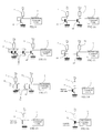
- a load 1 has a first terminal connected to a supply voltage Va and a second terminal connected to the anode of a diode 2, the cathode of this diode 2 being connected to ground.
- the voltage across the diode is representative of the current flowing through it, the correspondence through the characteristic of this diode. So an entry from the fuzzy logic processor 3 is connected to the anode of the diode 2.
- the charge 2 can be of different types and that it is also possible to add protective elements to fuzzy processor input 3.
- the first area corresponds to the breakdown of the diode which can be destructive if the diode is not planned for that.
- a diode with a Vc (breakdown voltage in reverse given by the manufacturer) such as the case can't show up.
- the second domain corresponds to a blocked diode, the current is an almost zero leakage current.
- the third area corresponds to the switching of the diode. An approximation of this area is a exponential.
- the fourth domain corresponds to a diode busy. This area is very close to a straight line and the manufacturer gives the threshold voltage Vs which corresponds at the voltage of the Thévenin model of the diode as well as the resistance of the diode which will give the slope of the right. Classically the manufacturer gives the values typical and extreme of these two parameters which depending on the diodes, an error of 5 to 20%.
- the fifth domain corresponds to a dissipation power in the diode too high which will cause destruction of the diode.
- manufacturers gives a maximum current value Imax with a safety factor.
- diodes are used with voltages greater than -Vc and with currents lower than Imax.
- the currents that interest us are between 0 A and Imax.
- membership functions 4, 5 and 6 represented on Figure 4.
- the first membership function 4 equals "1" for all voltages less than or equal to 0 V, decreases linearly up to “0” for a voltage equal to V1, and is worth “0” for the voltages higher than V1.
- the second membership function 5 equals "0” for voltages less than 0 V or greater than V2, increases linearly from “0” to “1” for voltages ranging from 0V to V1, and decreases linearly from “1” to "0” for voltages going from V1 to V2.
- the third membership function is worth “0” for the tensions lower than V1, believes linearly from “0” to "1” for voltages ranging from V1 at V2, and is worth 1 for voltages higher than V2.
- the first threshold corresponding to 0 V is independent of the diode; it will therefore be fixed when programming the membership functions and decision rules.
- the thresholds V1 and V2 are fixed on a test bench. On the bench of tests, it is enough to substitute for load 1 a variable load provided with calibration means allowing fix the currents I1 and Imax. When each of currents is well established, we store in memory from the processor blurs the corresponding voltage value.
- the fourth membership function 7 is worth “1" for all voltages less than or equal to 0 V, decreases linearly to "0” for a voltage between 0 V and V3, and equals "0" for voltages greater than V3.
- the fifth membership function 8 is "0" for voltages less than 0 V or greater than V4, increases linearly from “0” to “1” for voltages ranging from 0 V to V3, and decreases linearly from “1” to "0” for voltages ranging from V3 to V4.
- the sixth membership function 9 equals "0" for voltages lower than V3 or higher than V1, believes linearly from “0” to “1” for voltages ranging from V3 to V4, and decreases linearly from “1” to "0” for voltages ranging from V4 to V1.
- the seventh function belonging 10 equals "0" for lower voltages at V4 or higher than V2, increases linearly from “0” to “1” for voltages from V4 to V1, and decreases linearly from “1” to “0” for voltages ranging from V1 to V2.
- the thresholds V1, V2, V3 and V4 are memorized by learning.
- Diode 2 can be replaced by a transistor bipolar 12 or a MOS transistor 13 mounted as a diode as can be seen in Figures 8 and 9.
- Figures 8 and 9 can be improved by using a current mirror to decouple the input of the fuzzy processor of the power supply Va, if this voltage is too high.
- Figure 10 we uses a so-called current mirror assembly.
- the second load terminal 1 is connected to the collector of a transistor 15 mounted as a diode, the emitter of this transistor 15 being connected to ground.
- a second charge 14 has a first terminal connected to the supply voltage Vcc of the fuzzy processor 3, a second terminal of this second load 14 being connected to the collector of a transistor 16.
- the transistor 16 has its base connected to the base of the transistor 15, the emitter of transistor 16 being connected to the mass (the mass is common to the two power supplies).
- the fuzzy logic processor measures the voltage of collector of transistor 16.
- a current mirror is constituted with the two transistors 15 and 16 if these two transistor are strictly identical in dimensions (preferably on the same substrate).
- the current mirror device has as disadvantage of consuming in the second charge 14 a considerable current. It is possible to reduce this consumption by adding several transistors 17 mounted in parallel with transistor 15, all these transistors 15, 16 and 17 must have the same dimensions. Such assembly is shown in Figure 11. It would better to use a matrix of transistors identical using the same substrate, one of the transistors would be used to draw current. Such device to divide the current in the load 14 by the number of transistors 15 and 17 used. It is also possible to use a larger transistor 15 than transistor 16, but the accuracy is less.
- Transposition with MOS transistors is done automatically by replacing transistors 15, 16 and 17 by MOS transistors 18, 19 and 20.
- Figures 12 and 13 are equivalent to FIGS. 10 and 11.
- Another benefit of using a non-element linear to perform the current measurement is to use a component used to switch the load 1 to perform the measurement. So in the figure 14, we can see the load 1 which is switched by a transistor 21 serving as a switch between a voltage supply Va and the mass according to a signal of ordered.
- the voltage measurement made by the processor at fuzzy logic 3 can be done on the collector of the transistor 21 or on the basis of transistor 21.
- the choice collector or base as measuring point depends in fact of the importance of the current to be measured. If this one is small, the voltage variations on the base are only not large enough to measure current and it is therefore preferable to measure on the collector. If we use a MOS transistor 22 as in FIG. 15, the voltage measurement is obviously made on the drain.
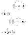
- the second load terminal 1 is connected to the anode of the thyristor 23, the cathode of this thyristor 23 being connected to the mass.
- a control signal is sent to the trigger thyristor 23.
- the measured voltage will be preferably the voltage of the PN junction of the thyristor 23 whose N-doped zone is connected to the mass.
- FIG 17 is shown the thyristor 23.
- a left we can see a schematic representation in chopped off.
- the four N and P alternating doping layers are represented by rectangles.
- the layer P taken between the two layers N has no bound bound outside.
- performing the measurement on S allows protect the input of the fuzzy logic processor 3 against tensions that could be destructive.
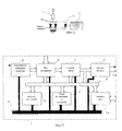
- the control circuit 37 performs a sequencing of the processor which consists in sampling and converting data entering on converter 30 or entering directly on the register block, then scroll down the different decision rules, checking each time times membership in membership functions corresponding to these rules. In an operation normal, the control circuit 37 therefore alternates input parameters day and rule sweep. Obviously a result is given at the end of the scan rules.
- the control circuit will also take care information transfers with the outside via the serial interface which allow to have particular operations of processor 3, in particular recording of the various parameters.
- fuzzy logic processor is already marketed by the company known as SGS-THOMSON MICROELECTRONICS under the name of W.A.R.P. 3.
- fuzzy logic processors provide type membership functions trapezoid or Gaussian type.
- An improvement of the invention is to combine the linear approximation explained previously with half-Gaussians. The use of gaussians reduces the number of membership functions necessary to follow a curve without increasing the error, this amounts to performing a Gaussian interpolation.
- fuzzy processor inputs can be used for other parameters.
- decision of the fuzzy processor may be of a different type than the current value, for example a control signal for switch the charge.
- Measurement errors actually depend on the resolution of the analog / digital converter.
- the resolution is conventionally 1 or 1/2 least significant bit which makes the error less than 1/2 n (n being the number of bits on which the sampling takes place) times the maximum voltage deviation .
- the linear approximation of the curve also comes into play in the calculation of the error.
- the fuzzy logic processor may have an input for current measurement, a input for speed reference, one input for actual speed and determine, based on rules and membership functions of these three inputs, one decision which is the control of the transistor switching the engine.
Landscapes
- Physics & Mathematics (AREA)
- General Physics & Mathematics (AREA)
- Logic Circuits (AREA)
- Control Of Voltage And Current In General (AREA)
- Testing Of Individual Semiconductor Devices (AREA)
Claims (21)
- Schaltkreis zum Messen des Stromes durch eine Last (1), wobei der Schaltkreis ein nicht-lineares Element (2, 11, 13, 16, 19, 21, 22, 23, 24, 27 oder 28) zur Transformation eines Strom in eine Spannung umfaßt,
dadurch gekennzeichnet, daß
er einen Prozessor für unscharfe Logik (3) zum Verarbeiten einer Messung der genannten Spannung und zum Ausgeben einer Information in Abhängigkeit von dem Strom umfaßt. - Schaltkreis nach Anspruch 1, dadurch gekennzeichnet, daß das nicht-lineare Element ein Meßtransistor (13 oder 22) vom Typ MOSFET ist, dessen Source mit Masse verbunden ist und dessen Drain mit einem Eingang des Prozessors für unscharfe Logik (3) und einem Anschluß für die Last (1) verbunden ist.
- Schaltkreis nach Anspruch 1, dadurch gekennzeichnet, daß das Transformationselement ein Meßtransistor (19) vom Typ MOSFET ist, dessen Source mit Masse verbunden ist und dessen Drain mit einem Eingang des Prozessors für unscharfe Logik (3) und einem Vorspannungsschaltkreis (14) verbunden ist, und daß ein Zwischentransistor (18) über seinen Drain mit einem Anschluß für die Last, über seine Source mit der Masse und über sein Gate mit dem Gate des Meßtransistors (19) verbunden ist.
- Schaltkreis nach Anspruch 3, dadurch gekennzeichnet, daß der Zwischentransistor (18) parallel geschaltet ist zu mehreren Transistoren (20), deren Dimensionen identisch sind zu dem Zwischentransistor.
- Schaltkreis nach einem der Ansprüche 3 oder 4, dadurch gekennzeichnet, daß der Meßtransistor (19) die gleichen Dimensionen hat wie der Zwischentransistor (18).
- Schaltkreis nach einem der Ansprüche 2 bis 5, dadurch gekennzeichnet, daß bei dem Transistor (13, 18, 20), der mit der Last verbunden ist, der Drain mit seinem Gate verbunden ist.
- Schaltkreis nach einem der Ansprüche 2 bis 5, dadurch gekennzeichnet, daß bei dem Transistor (22), der mit der Last verbunden ist, das Gate mit einem Steuerschaltkreis verbunden ist und daß der genannte Transistor (22) als Unterbrecher genützt wird.
- Schaltkreis nach einem der Ansprüche 2 bis 7, dadurch gekennzeichnet, daß die MOSFET-Transistoren (13, 18, 19, 20, 22) ersetzt werden durch Bipolar-transistoren (12, 15, 16, 17 21).
- Schaltkreis nach Anspruch 1, dadurch gekennzeichnet, daß das Transformationselement eine Diode (2) ist.
- Schaltkreis nach Anspruch 1, dadurch gekennzeichnet, daß das Transformationselement aus zwei Dioden (2, 11) besteht, die parallel in jeweils umgekehrter Polarität geschaltet sind.
- Schaltkreis nach Anspruch 1, dadurch gekennzeichnet, daß das Transformationselement ein Meßthyristor (23, 27) ist, dessen Gate verbunden ist mit einem Steuersignal.
- Schaltkreis nach Anspruch 11, dadurch gekennzeichnet, daß der Meßthyristcr (27) parallel zu mehreren thyristoren (29) mit identischen Dimensionen geschaltet ist.
- Schaltkreis nach Anspruch 1, dadurch gekennzeichnet, daß das Transformationselement für den Strom ein Meßtriac (24, 28) ist, dessen Gate mit einem Steuersignal verbunden ist.
- Schaltkreis nach Anspruch 13, dadurch gekennzeichnet, daß der Meßtriac (28) parallel zu mehreren Triacs (26) mit identischen Dimensionen geschaltet ist.
- Schaltkreis nach einem der Ansprüche 1 bis 14, dadurch gekennzeichnet, daß der Prozessor für unscharfe Logik (3) einen nicht-flüchtigen Speicherbereich (33) umfaßt und Zugehörigkeitsfunktionen (4 bis 10) und Entscheidungsregeln für die Information, die von dem Strom abhängt, abglegt sind im nicht-flüchtigen Speicher (33).
- Schaltkreis nach Anspruch 15, dadurch gekennzeichnet, daß wenigstens eine der Zugeförigkeitsfunktionen (4 bis 10) vom Dreieckstyp sind.
- Schaltkreis nach Anspruch 16, dadurch gekennzeichnet, daß der Prozessor für unscharfe Logik (3) eine lineare Näherung einer Stromspannungsübertragungseigenschaft des nicht-linearen Elements durchführt.
- Schaltkreis nach Anspruch 15, dadurch gekennzeichnet, daß wenigstens eine der Zugehörigkeitsfunktionen vom Gauß-Typ ist.
- Schaltkreis nach einem der Ansprüche 15 bis 18, dadruch gekennzeichnet, daß der nicht-flüchtige Speicher Schwellenspannungen (V1, V2, V3 und V4) zum Begrenzen der Zugehörigkeitsfunktionen (4 bis 10) umfaßt, wobei die Schwellen (V1 bis V4) abgelegt werden in dem nicht-flüchtigen Speicher (33), wenn eine Eichung des Meßschaltkreises vorgenommen wird.
- Schaltkreis nach einem der Ansprüche 15 bis 19, dadurch gekennzeichnet, daß die Entscheidungsregeln eine Information bestimmen, die von dem Strom durch die Last abhängt.
- Schaltkreis nach einem der Ansprüche 15 bis 20, dadurch gekennzeichnet, daß der Prozessor für unscharfe Logik (3) mehrere Informationseingänge aufweist und daß die Entscheidungsregeln ein Steuersignal festlegen.
Applications Claiming Priority (2)
| Application Number | Priority Date | Filing Date | Title |
|---|---|---|---|
| FR9600402A FR2743635B1 (fr) | 1996-01-11 | 1996-01-11 | Circuit de mesure de courant |
| FR9600402 | 1996-01-11 |
Publications (2)
| Publication Number | Publication Date |
|---|---|
| EP0789246A1 EP0789246A1 (de) | 1997-08-13 |
| EP0789246B1 true EP0789246B1 (de) | 1998-11-18 |
Family
ID=9488123
Family Applications (1)
| Application Number | Title | Priority Date | Filing Date |
|---|---|---|---|
| EP96470025A Expired - Lifetime EP0789246B1 (de) | 1996-01-11 | 1996-12-11 | Strommessschaltung |
Country Status (4)
| Country | Link |
|---|---|
| US (1) | US5845275A (de) |
| EP (1) | EP0789246B1 (de) |
| DE (1) | DE69600991T2 (de) |
| FR (1) | FR2743635B1 (de) |
Cited By (1)
| Publication number | Priority date | Publication date | Assignee | Title |
|---|---|---|---|---|
| CN106841764A (zh) * | 2016-12-28 | 2017-06-13 | 东莞泰克威科技有限公司 | 一种利用mosfet管内阻作为输出电流检测的方法 |
Families Citing this family (11)
| Publication number | Priority date | Publication date | Assignee | Title |
|---|---|---|---|---|
| FR2759799B1 (fr) * | 1997-02-18 | 1999-04-30 | Sgs Thomson Microelectronics | Procede d'utilisation en reseau d'un processeur de logique floue, et processeur de logique floue utilisable en reseau |
| US6310439B1 (en) * | 1999-03-15 | 2001-10-30 | Lutron Electronics Company, Inc. | Distributed parallel semiconductor device spaced for improved thermal distribution and having reduced power dissipation |
| JP3510546B2 (ja) * | 1999-12-01 | 2004-03-29 | Necエレクトロニクス株式会社 | Mosトランジスタのゲート酸化膜トンネル電流モデル |
| US6563080B2 (en) * | 2001-02-15 | 2003-05-13 | Scimed Life Systems, Inc. | Laser cutting of stents and other medical devices |
| EP1450168B1 (de) * | 2003-02-24 | 2007-08-01 | ELMOS Semiconductor AG | Elektrische Schaltung zum Treiben einer Last |
| US6927546B2 (en) | 2003-04-28 | 2005-08-09 | Colorado Vnet, Llc | Load control system and method |
| DE102004059960A1 (de) * | 2004-12-13 | 2006-06-22 | Bourns, Inc., Riverside | Schaltungsanordnung zur Messung eines elektrischen Stromes |
| US20070132371A1 (en) * | 2005-12-12 | 2007-06-14 | General Electric Company | Color tunable light-emitting devices and method of making the same |
| DE102006058879A1 (de) * | 2006-12-13 | 2008-06-26 | Siemens Ag | Messvorrichtung zur Messung eines elektrischen Stromes |
| CN103412186A (zh) * | 2013-08-27 | 2013-11-27 | 国家电网公司 | 一种环网柜电流采集装置 |
| US10152276B2 (en) * | 2016-07-18 | 2018-12-11 | Winbond Electronics Corporation | Memory device including data processor and program method of same |
Family Cites Families (4)
| Publication number | Priority date | Publication date | Assignee | Title |
|---|---|---|---|---|
| US4553084A (en) * | 1984-04-02 | 1985-11-12 | Motorola, Inc. | Current sensing circuit |
| US4599554A (en) * | 1984-12-10 | 1986-07-08 | Texet Corportion | Vertical MOSFET with current monitor utilizing common drain current mirror |
| IT1213415B (it) * | 1986-12-17 | 1989-12-20 | Sgs Microelettronica Spa | Circuito per la misura lineare della corrente circolante su un carico. |
| EP0581993B1 (de) * | 1992-08-07 | 1995-03-15 | Siemens Aktiengesellschaft | Schaltungsanordnung zum Steuern einer Last und zum Erkennen einer Leitungsunterbrechung |
-
1996
- 1996-01-11 FR FR9600402A patent/FR2743635B1/fr not_active Expired - Fee Related
- 1996-12-11 DE DE69600991T patent/DE69600991T2/de not_active Expired - Fee Related
- 1996-12-11 EP EP96470025A patent/EP0789246B1/de not_active Expired - Lifetime
-
1997
- 1997-01-07 US US08/780,430 patent/US5845275A/en not_active Expired - Lifetime
Cited By (2)
| Publication number | Priority date | Publication date | Assignee | Title |
|---|---|---|---|---|
| CN106841764A (zh) * | 2016-12-28 | 2017-06-13 | 东莞泰克威科技有限公司 | 一种利用mosfet管内阻作为输出电流检测的方法 |
| CN106841764B (zh) * | 2016-12-28 | 2019-07-19 | 东莞泰克威科技有限公司 | 一种利用mosfet管内阻实现输出电流检测的方法 |
Also Published As
| Publication number | Publication date |
|---|---|
| FR2743635B1 (fr) | 1998-03-06 |
| DE69600991T2 (de) | 1999-07-01 |
| EP0789246A1 (de) | 1997-08-13 |
| FR2743635A1 (fr) | 1997-07-18 |
| DE69600991D1 (de) | 1998-12-24 |
| US5845275A (en) | 1998-12-01 |
Similar Documents
| Publication | Publication Date | Title |
|---|---|---|
| EP0789246B1 (de) | Strommessschaltung | |
| EP0578526B1 (de) | Hochspannungsschaltkreis | |
| EP0568439B1 (de) | Detektionsverfahren und -schaltung für Stromverluste in einer Bitleitung | |
| EP0793327B1 (de) | Vorrichtung zur Steuerung der Ladung mindestens einer Batterie | |
| US9299746B2 (en) | Select device for cross point memory structures | |
| FR2781285A1 (fr) | Dispositif de mesure automatique d'une resistance | |
| FR2697673A1 (fr) | Circuit à fusible, pour circuit intégré. | |
| EP0251853A1 (de) | Integrierte Schaltung zur Speicherung und zur vertraulichen Verarbeitung von Informationen, die eine Antibetrugsvorrichtung enthält | |
| FR2629248A1 (fr) | Procede de test de memoire a programmation unique et memoire correspondante | |
| FR3113777A1 (fr) | Alimentation de circuit électronique | |
| FR2535552A1 (fr) | Appareil et procede pour la synthese d'un signal d'excitation destine au test actif d'un circuit integre | |
| EP0675503A1 (de) | Integrierter Speicher mit Spaltenspannungserhaltungsschaltung | |
| FR3113776A1 (fr) | Alimentation de circuit électronique | |
| EP0500461A1 (de) | Anordnung für die Detektion des logischen Zustandes eines Bauteiles, dessen Impedanz sich in Abhängigkeit von seinen Zustand ändert | |
| EP0883102B1 (de) | Methode zur Kompensation von Störungen in einer kapazitiven Schaltung und Anwendung in Matrixanzeigevorrichtungen | |
| EP0703584B1 (de) | Adressen-Dekodierverfahren für einen integrierten Speicher und Speicherschaltung zur Anwendung eines solchen Verfahrens | |
| EP2333703B1 (de) | Elektronische Komponente zum Aufspüren von aktiven Angriffen | |
| EP3233576A1 (de) | Verfahren und vorrichtung zur diagnose einer vorrichtung zur verwaltung von elektrischer energie | |
| EP0506531A1 (de) | Schaltung zur Überwachung eines oberen Schwellwertes einer Versorgungsspannung | |
| FR2793064A1 (fr) | Memoire a courant de fuite reduit | |
| FR2811164A1 (fr) | Circuit integre avec dispositif de protection | |
| FR2830329A1 (fr) | Circuit de detection de tension pour dispositifs d'accumulation | |
| EP0159263B1 (de) | Verfahren und Vorrichtung zur Kontrolle des Flüssigkeitsstandes in einem Tank | |
| EP1400887A1 (de) | Schutzgerät für einen elektronischen Chip, der vertaulichen Informationen enthält | |
| US11508438B1 (en) | RRAM filament location based on NIR emission |
Legal Events
| Date | Code | Title | Description |
|---|---|---|---|
| PUAI | Public reference made under article 153(3) epc to a published international application that has entered the european phase |
Free format text: ORIGINAL CODE: 0009012 |
|
| 17P | Request for examination filed |
Effective date: 19970428 |
|
| AK | Designated contracting states |
Kind code of ref document: A1 Designated state(s): DE FR GB IT |
|
| 17Q | First examination report despatched |
Effective date: 19970715 |
|
| GRAG | Despatch of communication of intention to grant |
Free format text: ORIGINAL CODE: EPIDOS AGRA |
|
| GRAG | Despatch of communication of intention to grant |
Free format text: ORIGINAL CODE: EPIDOS AGRA |
|
| GRAH | Despatch of communication of intention to grant a patent |
Free format text: ORIGINAL CODE: EPIDOS IGRA |
|
| GRAH | Despatch of communication of intention to grant a patent |
Free format text: ORIGINAL CODE: EPIDOS IGRA |
|
| GRAA | (expected) grant |
Free format text: ORIGINAL CODE: 0009210 |
|
| AK | Designated contracting states |
Kind code of ref document: B1 Designated state(s): DE FR GB IT |
|
| GBT | Gb: translation of ep patent filed (gb section 77(6)(a)/1977) |
Effective date: 19981119 |
|
| REF | Corresponds to: |
Ref document number: 69600991 Country of ref document: DE Date of ref document: 19981224 |
|
| ITF | It: translation for a ep patent filed | ||
| RAP4 | Party data changed (patent owner data changed or rights of a patent transferred) |
Owner name: STMICROELECTRONICS S.A. |
|
| PLBE | No opposition filed within time limit |
Free format text: ORIGINAL CODE: 0009261 |
|
| STAA | Information on the status of an ep patent application or granted ep patent |
Free format text: STATUS: NO OPPOSITION FILED WITHIN TIME LIMIT |
|
| 26N | No opposition filed | ||
| REG | Reference to a national code |
Ref country code: GB Ref legal event code: IF02 |
|
| PGFP | Annual fee paid to national office [announced via postgrant information from national office to epo] |
Ref country code: GB Payment date: 20041208 Year of fee payment: 9 Ref country code: FR Payment date: 20041208 Year of fee payment: 9 |
|
| PGFP | Annual fee paid to national office [announced via postgrant information from national office to epo] |
Ref country code: DE Payment date: 20041209 Year of fee payment: 9 |
|
| PG25 | Lapsed in a contracting state [announced via postgrant information from national office to epo] |
Ref country code: IT Free format text: LAPSE BECAUSE OF NON-PAYMENT OF DUE FEES Effective date: 20051211 Ref country code: GB Free format text: LAPSE BECAUSE OF NON-PAYMENT OF DUE FEES Effective date: 20051211 |
|
| PG25 | Lapsed in a contracting state [announced via postgrant information from national office to epo] |
Ref country code: DE Free format text: LAPSE BECAUSE OF NON-PAYMENT OF DUE FEES Effective date: 20060701 |
|
| GBPC | Gb: european patent ceased through non-payment of renewal fee |
Effective date: 20051211 |
|
| PG25 | Lapsed in a contracting state [announced via postgrant information from national office to epo] |
Ref country code: FR Free format text: LAPSE BECAUSE OF NON-PAYMENT OF DUE FEES Effective date: 20060831 |
|
| REG | Reference to a national code |
Ref country code: FR Ref legal event code: ST Effective date: 20060831 |