EP0786353A1 - Led printing head - Google Patents
Led printing head Download PDFInfo
- Publication number
- EP0786353A1 EP0786353A1 EP95933619A EP95933619A EP0786353A1 EP 0786353 A1 EP0786353 A1 EP 0786353A1 EP 95933619 A EP95933619 A EP 95933619A EP 95933619 A EP95933619 A EP 95933619A EP 0786353 A1 EP0786353 A1 EP 0786353A1
- Authority
- EP
- European Patent Office
- Prior art keywords
- led
- lens array
- aforementioned
- array
- light
- Prior art date
- Legal status (The legal status is an assumption and is not a legal conclusion. Google has not performed a legal analysis and makes no representation as to the accuracy of the status listed.)
- Granted
Links
Images







Classifications
-
- B—PERFORMING OPERATIONS; TRANSPORTING
- B41—PRINTING; LINING MACHINES; TYPEWRITERS; STAMPS
- B41J—TYPEWRITERS; SELECTIVE PRINTING MECHANISMS, i.e. MECHANISMS PRINTING OTHERWISE THAN FROM A FORME; CORRECTION OF TYPOGRAPHICAL ERRORS
- B41J2/00—Typewriters or selective printing mechanisms characterised by the printing or marking process for which they are designed
- B41J2/435—Typewriters or selective printing mechanisms characterised by the printing or marking process for which they are designed characterised by selective application of radiation to a printing material or impression-transfer material
-
- B—PERFORMING OPERATIONS; TRANSPORTING
- B41—PRINTING; LINING MACHINES; TYPEWRITERS; STAMPS
- B41J—TYPEWRITERS; SELECTIVE PRINTING MECHANISMS, i.e. MECHANISMS PRINTING OTHERWISE THAN FROM A FORME; CORRECTION OF TYPOGRAPHICAL ERRORS
- B41J2/00—Typewriters or selective printing mechanisms characterised by the printing or marking process for which they are designed
- B41J2/435—Typewriters or selective printing mechanisms characterised by the printing or marking process for which they are designed characterised by selective application of radiation to a printing material or impression-transfer material
- B41J2/465—Typewriters or selective printing mechanisms characterised by the printing or marking process for which they are designed characterised by selective application of radiation to a printing material or impression-transfer material using masks, e.g. light-switching masks
-
- B—PERFORMING OPERATIONS; TRANSPORTING
- B41—PRINTING; LINING MACHINES; TYPEWRITERS; STAMPS
- B41J—TYPEWRITERS; SELECTIVE PRINTING MECHANISMS, i.e. MECHANISMS PRINTING OTHERWISE THAN FROM A FORME; CORRECTION OF TYPOGRAPHICAL ERRORS
- B41J2/00—Typewriters or selective printing mechanisms characterised by the printing or marking process for which they are designed
- B41J2/435—Typewriters or selective printing mechanisms characterised by the printing or marking process for which they are designed characterised by selective application of radiation to a printing material or impression-transfer material
- B41J2/447—Typewriters or selective printing mechanisms characterised by the printing or marking process for which they are designed characterised by selective application of radiation to a printing material or impression-transfer material using arrays of radiation sources
- B41J2/45—Typewriters or selective printing mechanisms characterised by the printing or marking process for which they are designed characterised by selective application of radiation to a printing material or impression-transfer material using arrays of radiation sources using light-emitting diode [LED] or laser arrays
- B41J2/451—Special optical means therefor, e.g. lenses, mirrors, focusing means
Definitions
- This invention relates to LED print heads which utilize light signals emitted from LED's to form latent images for graphic image formation.
- LED printers and laser printers using light emitting diode (LED) heads, semi-conductor laser heads, etc., to generate light signals which are irradiated onto the surface of light-sensitive materials to form static latent images from which printed graphic images are formed on printing materials are already well known.
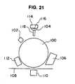
- Such LED printers consist of: a charging device 102 which electrifies the surface of a revolving light-sensitive drum 100; an LED print head 104 which irradiates light to form static latent images in accordance with the input signals, i.e., the electric signals on the charged light-sensitive drum 100; a processing device 106 to process the static latent images; a transcriber 110 to transfer toner, the image formation medium, onto the printing material 108, which is moved in accordance with the revolution of the light sensitive drum 100; a fixing device (not shown in drawing) to fix the toner that is transferred onto the printing material 108 by heating, etc.; and a cleaner 112 to clean the surface of the light-sensitive drum 100.
- An LED print head 104 used in such LED printers consists of a substrate 114 on which is formed an electrical circuit, an LED array 116 consisting of LED's which are formed on the substrate and which generate light in accordance with the applied electric signals, and a rod-lens array 118 consisting of cylindrical lenses which condense light generated from the LED array 116 onto the light-sensitive drum 100. These components are assembled in such a way that light generated from the LED array 116 is condensed onto the surface of the electrified light-sensitive drum 100 by means of the rod-lens array 118, such that latent images for graphic images to be formed on the printing material 108 are formed on the light-sensitive drum 100.
- the LED array 116 on the LED print head 104 consists of LED array chips 16a, 16b, etc., set apart by a certain distance l, each chip having a certain number of LED's arranged at a certain pitch P.
- the LED array chips 16a, 16b, etc. consist of a chip substrate 122 and a number of light-emitting elements, LED's 124, which are formed on the surface of the chip substrate 122.
- An electrode 126 made of a conducting metal is connected to the surface of each LED 124. At the other end of the electrode 126 is formed a pad electrode 128, which is electrically connected via a wire (not shown in drawing) to a driver IC (not shown in drawing) mounted on the substrate 114.
- a pitch P of approximately 42 ⁇ m for the LED's 124 on LED array chips 16a, 16b, etc. is necessary, 20 ⁇ m being the columnwise width W of an LED 124 of conventional size.
- the clearance l between LED array chips 16a, 16b, etc. would be approximately 6 ⁇ m.
- LED print heads 104 In attempting to manufacture LED print heads 104 with above a certain level of resolution, since dimensional errors in cutting a chip substrate stick into LED array chips 16a, 16b, etc. and errors in die bonding onto circuit substrates inevitably occur during the manufacturing process, and particularly since it is extremely difficult to set the LED's 124 on the end of neighboring LED array chips 16a, 16b, etc. such that the distance or pitch between them is identical to that between the other LED's 124, that is, since it is extremely difficult to manufacture LED array chips 16a, 16b, etc. such that all the LED's 124 are formed at a fixed pitch at high density, it has not been possible to satisfy the demand for affordable high resolution LED print heads.
- the object of the invention is to provide an LED print head with improved resolution using relatively simple methods.
- the first aspect of the invention is characterized in that the LED print head comprises: LED arrays consisting of LED's arranged in one direction such that selective generation of light signals is possible; a light-sensitive object positioned along an axis parallel to the aforementioned LED arrays such that it can be rotated; lens arrays arranged such that light signals generated from the aforementioned LED's are condensed onto the aforementioned light-sensitive material; and optical shutters positioned with respect to the aforementioned lens arrays such that they can be switched to channel light signals from a designated aforementioned LED array to a designated aforementioned lens array.
- the lens arrays comprises of a first and a second lens array, the first lens array consisting of lenses with central optical axes tilted at a slight angle toward one side of the main scanning direction, and the second lens array consisting of lenses with central optical axes tilted at a slight angle toward the side opposite that of the tilt of the lens of the first lens array.
- the lens arrays comprises a first and a second lens array, the first lens array consisting of lenses with central optical axes tilted at a slight angle toward one side of the main scanning direction, and the second lens array consisting of lenses with central optical axes which do not tilt to either side of the main scanning direction.
- an LED print head of the second or third aspect wherein the first and second lens arrays are arranged at a slight angle to form a V or inverted V configuration as viewed from the main scanning direction.
- an LED print head of the first aspect wherein the lens arrays comprises a first and a second lens array, with the first and second lens arrays positioned to cross at a slight angle in such a way that their lengthwise sides form a certain angle relative to each other.
- an LED print head of the first aspect wherein the LED arrays comprises a first and a second LED array, the aforementioned first and second LED arrays comprising LED's set at a certain pitch respectively and at a half-pitch relative to each other in the main scanning direction.
- an LED print head of the first aspect wherein the optical shutter is a liquid crystal shutter utilizing a ferroelectric liquid crystal.
- an LED print head of the first aspect wherein the optical shutter is an optical shutter utilizing electro-optic ceramics.
- an LED print head comprising, LED arrays with at least a first and a second array of LED's; a driver IC electrically connected to the first and second arrays of LED's; lens arrays consisting of lenses arranged to condense onto the light-sensitive surface light signals generated from LED's responding to electric signals from the driver IC; and a switching device set between the common electrical wiring of the first LED array and that of the second LED array.
- an LED print head of the ninth aspect wherein the LED's of the first LED array and the second LED array are set at a certain pitch respectively and at a half-pitch relative to each other in the main scanning direction.
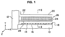
- FIG. 1 Shown in FIG. 1 are the main elements of an LED print head according to the first embodiment of the invention. A cross-sectional view along line - of FIG. 1 is shown in FIG. 2.
- the substrate 10 is made of glass epoxy material, and is fixed to a housing 12 which holds the main elements of the LED print head. Circuits consisting of semiconductors are formed on the surface of the substrate 10 as required.
- LED array chips 16 comprising a plurality of LED's 14 arranged at a certain pitch are set in a row at a certain distance from each other, and the LED's 14 positioned continuously at a fixed pitch in the main scanning direction (the X-axis in FIG. 1) form LED array 18.
- the LED array chips 16 are electrically connected via bonding wires 17 to driver IC's 50 (FIG. 2), which are positioned parallel to the array chips.
- the LED array 18 is a cylindrical light-sensitive drum 22, attached to a housing 12 such that it rotates along the X-axis, and formed from a light-sensitive surface 20 onto which light signals generated from the LED's 14 are irradiated.
- the rod-lens array 26 which consists of cylindrical rod lenses 24 with focal lengths that allow for light from each LED 14 to form an image on the light-sensitive surface 20, and which is separated from the LED array 18 by a certain distance.
- Each rod-lens array 26 consists of two lens arrays: a first lens array 26a, wherein each rod lens 24 is slightly tilted toward one side of the X-axis direction at an angle ⁇ with respect to the perpendicular line that passes through the center of the light emission surface of each LED 14, that is, the Y-axis which is perpendicular to both the main scanning direction (X-axis) and the secondary scanning direction (Z-axis); and a second lens array 26b which is slightly tilted at an angle ⁇ with respect to the Y-axis in the direction opposite to that of the aforementioned direction.
- first lens array 26a and the second lens array 26b of the preferred embodiment are arranged such that each is tilted at an angle ⁇ toward the X-axis direction, the invention is not restricted to this configuration, and a configuration in which each lens of the second lens array 26b is not tilted is also possible.
- the optical shutters 28 comprising two rows, the first and the second optical shutters 28a, 28b, corresponding to the first lens array 26a and the second lens array 26b.
- the optical shutter 28 is a liquid crystal shutter comprising a ferroelectric crystal 36 sandwiches in between an upper substrate 32, on which transparent electrodes 30a and 30b are formed opposite each other and which is made of glass, and a lower substrate 34 on which a transparent electrode 30c opposite to the transparent electrodes 30a, 30b, is formed.
- Polarizing plates 38 are adhered to the outer surfaces of both upper and lower substrates 32 and 34.
- the optical shutter 28 is a combination of two parts: the shutter area on the left side of FIG. 4, consisting of transparent electrodes 30a and 30c which form the first optical shutter 28a, and the shutter area on the right side of FIG. 4, consisting of transparent electrodes 30b and 30c which form the second optical shutter 28b.
- transparent electrodes 30a and 30b are electrically connected to a signal source via a switching circuit not shown in the drawing, and transparent electrode 30c is electrically connected to a signal source via electrical wiring.
- the opening and shutting of the first and second optical shutters 28a and 28b are performed synchronously with the selective irradiation of the LED's 14 through the driver IC's 50.
- the rod lenses 24 of the first lens array 26a are positioned such that the central optical axes 40 are tilted to one side at an angle ⁇ , as shown in FIG. 5 (a). Therefore, when a light signal is generated from an arbitrary LED 14a, and the corresponding first optical shutter 28a is opened and the adjacent optical shutter 28b shut, the light signal forms, via the first lens array 26a, an image on light-sensitive surface 20 at position A 1 displaced in the direction of the tilt of the central optical axis by distance ⁇ .
- the central optical axes 40 of the rod lenses 24 of the second lens array 26b are tilted at an angle ⁇ to the side opposite the aforementioned side. Therefore, when a light signal is generated from the aforementioned LED 14a, the corresponding second optical shutter 28b is opened and the first optical shutter 28a shut, the light signal forming, via the second lens array 26b, an image on the light-sensitive surface 20 at position B 1 displaced in the direction of the tilt of the central optical axis by distance ⁇ .
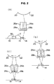
- first and the second lens arrays 26a and 26b are positioned parallel to each other as seen from the direction of the X-axis (see FIG. 2 (a)), light from a single LED 14 will form images at an identical position via lens arrays 26a and 26b. Therefore, when the light-sensitive drum is rotating at a fixed speed, the latent image formed on light-sensitive surface 20 via the second lens array 26b will not fall on the same line as the latent image formed via the first lens array 26a, but will form a zigzag line.
- the first and the second lens arrays 26a and 26b as seen from the direction of the X-axis are arranged at a slight angle such that they form an inverted V- or a V-shape, as shown in FIG. 2 (b) and FIG. 2 (c).
- the latent image formed via the second lens array 26b is formed after the latent image formed via the first lens array 26a has been displaced a certain distance in accordance with the rotation of the light-sensitive drum 22, and it is possible to arrange the latent images on the same line.
- FIG. 2 (c) given that the rotational direction of light-sensitive drum 22 is identical to that of FIG.
- LED array 18 with LED's 14 set at a certain pitch can be used to obtain graphic images with double pixel density or resolution.
- the pitch P of the LED's 14 will be 84.6 ⁇ m, and substituting in the equation above yields 21.15 ⁇ m for ⁇ .
- liquid crystal shutters using ferroelectric liquid crystals were used as optical shutters 28, it is also possible to use instead optical shutters using an electro-optic ceramic material known as PLZT shown in FIG. 6 or the mechanical optical shutter shown in FIG. 7.
- the optical shutter made of PLZT shown in FIG. 6 comprises PLZT 46 sandwiches between an upper plate of glass substrate 52 on which transparent electrodes 44a and 44b are formed opposite each other with silicon rubber in between and a lower plate of glass substrate 54 on which a transparent electrode 44c is formed with silicon rubber 42 in between.
- Polarizing plates 48 are adhered to the outer surfaces of the upper and lower substrates 52 and 54.
- this optical shutter is also a combination of two parts, namely: the shutter area on the left side of FIG. 6, consisting of transparent electrodes 44a and 44c which form the first optical shutter 28a, and the shutter area on the right side of FIG. 6, consisting of transparent electrodes 44b and 44c which form the second optical shutter 28b.
- the opening and shutting of the first and second optical shutters 28a and 28b are performed by synchronization with the selective irradiation of the LED's 14 through driver IC's.
- FIG. 7 (a) shows the structure of a mechanical optical shutter that can be used in the invention.
- This optical shutter consists of a light-shielding plate 58 positioned below the first and second lens arrays 26a and 26 b which rotates 180° , for instance, around a shaft 56 in response to an electric signal from a driver IC 50.
- FIG. 7(b) shows an optical shutter consisting of a light-shielding plate 64 positioned below the first and second lens arrays 26a and 26 b which is held in position by a spring 62 which can be moved along the Z-axis using a solenoid 60 which is controlled via electrical signals from a driver IC.
- Such mechanical optical shutters can be used as optical shutters 28 by synchronizing emissions from the LED's 14 of the LED array 18 so that light signals are irradiated via the first lens array 26a or the second lens arrays 26b onto the light-sensitive surface as a result of the shutters.
- the respective rod lenses of the first and the second lens arrays 26c and 26d form a certain angle ⁇ on both sides of the aforementioned Y-axis. In other words, they form the angle 2 ⁇ with respect to each other.
- the optical shutter 28 Installed in the housing 12 together with the first and the second lens arrays 26c and 26d is the optical shutter 28 consisting of corresponding first and second optical shutters 28c and 28d.
- the arrangement is identical to that of the first preferred embodiment.
- pixel latent images formed by combining light signals from LED's 14 using a first lens array 26c and a second lens array 26d are possible.
- LED array 18 with LED's 14 of a certain pitch the formation of images of double resolution is possible.
- the lenses of the first and the second lens arrays are arranged such that they tilt in opposite directions from each other, configurations involving the tilting of the lens of one lens array without the tilting of the lens of the other lens array are also possible.
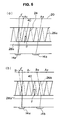
- FIG. 9 shows a perspective view of a rod-lens array 26 according to the third preferred embodiment.
- the rod-lens array 26 comprises a pair of board-shaped structural supports 66 made of glass-epoxy type material elongated in a lengthwise direction of rod-lens array 26, a plurality of cylindrical rod lenses 24 placed between the support 66, and spacers 68 fixed at both ends of the rows of rod lenses in between the support 66.
- the plurality of rod lenses 24 are tilted slightly in the lengthwise direction of the support material 66 at a certain angle to one side and are fixed in position using epoxy resin.
- the rod lenses 24 shown in the example in FIG. 9 are arranged in a zigzag fashion.
- a circuit substrate 10 with an electric circuit formed on its surface is fixed to the housing 12 which is made of resin.
- an LED array with LED's arranged at a certain pitch for light emission as well as driver IC's to drive the LED's is mounted on the substrate 10.
- the other support axis 70 is connected to a revolving axis of a revolving mechanism 72, and rod-lens array 26 rotates around the rotational axis X 1 which passes through the support axis 70 due to the rotational drive of the revolving mechanism 72.
- An LED print head of this construction condenses the light generated from the LED array via the rod-lens array 26, and stays at a fixed position relative to the light-sensitive drum 22 which revolves around an axis parallel to revolving axis X 1 .
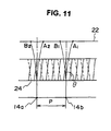
- the rod-lens array 26 of the third preferred embodiment consists of rod lenses 24 with optical axes that are slightly tilted in the lengthwise direction at a slight angle of ⁇ . Therefore, the direction of the tilt reverses every 180° rotation.
- the rod lens 24 in such a position as shown by the solid line in FIG. 11, if light is emitted from LED 14a which is set at a certain pitch P, the direction of the light will be changed as it follows the central optical axis of rod lens 24, and will form an image on the light-sensitive drum 22 at position A 1 displaced a certain distance to one side. At this time, if light is also emitted from adjacent LED 14b, it will also form an image on light-sensitive drum 22 at position A 2 also displaced a certain distance to one side.
- FIG. 12 shows a lengthwise cross-sectional view of the LED print head of the fourth preferred embodiment.
- the LED print head comprises: a substrate 10 made of glass-epoxy type material with the necessary elements for the electric circuit formed on the surface; an LED array (not shown) with a connection on the substrate 10 to the electric circuit, the LED's being arranged at a certain pitch; a rod-lens array 26 which is set apart from the LED array and which consists of a row of rod lenses which can be rotated by a slight angle; a casing 74 to keep the substrate 10 and the rod-lens array 26 at a certain position relative to each other; and a shifting mechanism 76 installed between the casing 74 and the rod-lens array 26 to rotate the rod-lens array 26 in accordance with electric signals from an electric circuit.
- a light-sensitive drum 22 which rotates at a certain speed along an axis parallel to the arranging direction (the lengthwise direction) of the LED array, i.e., the main scanning direction.
- the rod-lens array 26 comprises a pair of board-shaped structural supports 66 made of glass-epoxy type material, a plurality of cylindrical rod lenses 24 placed between the support material 66 (in the embodiment of FIG. 13, the rod lenses are arranged in a zigzag configuration), and spacers 68 fixed at both ends of the row of rod lens 24, in between the support 66.
- the rod-lens array 26 is held by holder 80 such that it is free to rotate. That is, referring back to FIG. 12, axis 78 which lies in the secondary scanning direction of rod-lens array 26 is fitted into the support holes 82 formed opposite each other in the secondary scanning direction at the center of the pair of lengthwise walls of the holder 80, which is of a simplified board shape made of resin.
- the rod-lens array 26 can therefore rotate with the secondary axis 78 as center.
- the shifting mechanism 76 is made from a piezoactuator formed by layering piezo-ceramics. It expands and contracts in accordance with an electric signal from the electric circuit on substrate 10, to which it is electrically connected. The expansion and contraction causes the rod-lens array 26 to rotate with the secondary scanning direction axis 78 as its center.
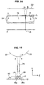
- the operation of the LED print head of the fourth embodiment is shown in FIG. 14.
- the home position for the rod-lens array 26 is the position parallel to the LED array, and this position is indicated by the solid line.
- line R in which the rod-lens array 26 tilts to one side at a slight angle ⁇ 1 , with the secondary scanning direction axis as the center, if a light signal is emitted from an arbitrary LED 14, the direction of the light signal will be changed as it follows the central optical axis of rod lens 24 of rod-lens array 26 and forms an image on the light-sensitive drum 22 at position A 1 displaced a certain distance to one side.
- a light signal emitted from the LED will likewise form an image at position B 1 displaced a certain distance to the other side of the main scanning direction.
- the LED print head of the fifth preferred embodiment comprises: a first LED array 18a and a second LED array 18b consisting of LED's arranged on substrate 10 in the direction of the X-axis at a certain pitch, with the LED's of the second array displaced a half pitch with respect to the LED's of the first array; a driver IC 50 set parallel to the first and the second LED arrays 18a and 18b and electrically connected to them via bonding wires 17; a light-sensitive drum 22 which can rotate around an axis parallel to the aforementioned first and second LED arrays 18a and 18b; a rod-lens array 26 which is positioned between the LED arrays 18a, 18b and the light-sensitive drum 22, and which condenses light signals indicated by the semi-dotted lines in the drawing generated by the first or the second LED array 18a or 18b onto the light-sensitive surface 20 of the light-sensitive drum 22 ; and an optical shutter 28 set under
- the rod-lens array 26 used in the fifth preferred embodiment, as in the second preferred embodiment, consists of a single rod-lens array of the conventional type without any tilt, and the same types of optical shutters as in the aforementioned embodiment can be utilized.
- the LED array of the fifth preferred embodiment consists of a first and a second LED array 18a and 18b
- the light signals emitted from all the LED's 14 are condensed onto the light-sensitive surface 20 via a common optical shutter 28 and rod-lens array 26.
- the first and the second LED arrays 18a and 18b are positioned such that they are slightly displaced in the Z-axis direction with respect to the central optical axis of each rod lens of the rod-lens array 26.
- rod-lens array is the rod-lens array with the product name SLA-20 sold by Nihon Itagarasu Kabushiki Kaisha.
- SLA-20 maintains a constant light intensity for a range within ⁇ 0.4 mm of the central optical axes of the lenses of the rod-lens array, and is therefore sufficient for the purposes of this embodiment.
- the LED's 14 of the first LED array 18a are made to emit light signals by the electrical signal from the driver IC 50.
- the light signals are condensed onto the light-sensitive surface 20 of light sensitive drum 22 at position A via the lens array 26, forming a pixel latent image.
- the LED's 14 of the second LED array 18b are made to emit light signals at the same time that the optical shutters are opened, with the result that a pixel latent image is formed on the light-sensitive surface 20 of the light-sensitive drum 22 at rotation position B, which lies on the same line as the pixel latent image formed at position A.
- the pixel latent images from the second LED array 18b are formed at a certain pitch at intermediary positions displaced a half-pitch with respect to the pixel latent images formed by the first LED array 18a, with both pixel latent images falling on the same line.
- FIG. 17 is a cross-sectional view showing the main parts of the LED print head of Preferred Embodiment 6.
- the first and the second LED arrays 18a and 18b are formed by displacing LED array chips 16a and 16b by a half pitch (P/2) with respect to each other, each thus being formed in a continuous configuration.
- the LED array chips 16a, 16b have a plurality of LED's 14 arranged at a fixed pitch P in the main scanning direction (X-axis direction).
- each LED array chips 16a and 16b is basically of the same structure as that of FIG. 22, for instance, the substrate 122 of the embodiment is of Gabs material, with a plurality of LED's formed in a row on the substrate 122.
- Each LED is formed by forming on the Gabs substrate 122 a GaAsP layer, on which a P-type diffusion layer 124, the light-emitting area, is formed by impurity diffusion using Zn.
- the electrode 126 is made of conducting material, and is electrically connected to the surface of the diffusion layer 124 at one end and has a pad 128 at the other end which can be connected via wire bonding to the circuit wiring of substrate 10.
- LED array chips 16a and 16b are positioned on the substrate with distance l between them such that the LED's are lined up in a row.
- the electrical connection between the LED's and the driver IC 50 of the LED arrays 18a and 18b is shown in FIG. 18.
- the anode of each LED of the first LED array 18a is electrically connected to the corresponding electrode pad of the driver IC, and the cathodes are connected to a common line, the first cathode line 84.
- the anode of each LED of the second LED array 18b is connected to the anode of the corresponding LED of the first LED array 18a, and the cathodes are connected to a common line, the second cathode line 86.
- the ends of first and second cathode lines 84 and 86 are connected to a switch 88 to allow for selective switching.
- first and the second LED arrays 18a and 18b is a cylindrical light-sensitive drum 22 with a light-sensitive surface 20 positioned to rotate along an axis in the X direction.
- the light signals generated by the LED's are irradiated onto the light-sensitive surface 20.
- a rod-lens array 26 consisting of a plurality of cylindrical rod lenses 24 with appropriate focal lengths such that the light from the LED's will form images on the light-sensitive surface 20.
- the rod-lens array 26 consists of rod lenses 24 which are positioned parallel to each other along the X-axis between the support 90, and is inserted together with the substrate 10 into the casing 92, which is made of resin.
- LED arrays 18a and 18 b are separated by distance D along the Y-axis from the light-sensitive surface, with the rod-lens array 26 positioned in between.
- the driver IC 50 sends an electric signal and, synchronized with the signal, the switch 88 is switched, selectively closing the circuit for the LED's of the first LED array 18a and causing the emission of light signals.
- the light signals are condensed at position A on the light-sensitive surface 20 of the light-sensitive drum 22 via the rod-lens array 26, and pixel latent images are formed along the scanning line. At this point, the circuit of the second LED array 18b is broken.
- the switch 88 is switched to the side of the second LED array 18b, breaking the circuit of the first LED array 18a and selectively closing the circuit for the second LED array 18b. This causes the LED's of the second LED array 18b to generate light signals, and a pixel latent image with a certain pitch is formed at position B on the light-sensitive surface 20.
- LED arrays 18a and 18b of the embodiment are formed from two rows of LED's. Therefore, for instance, if the zigzag configuration rod lens 24 is used for rod-lens array 26, depending on the distance settings, it may be necessary to shift the positions for LED array 18a and 18b slightly from the central optical axis in the Z-axis direction, and as a result the intensity of light passing through rod-lens array 26 may be insufficient.
- SLA-20 a rod-lens array sold by Nihon Itagarasu Kabushiki Kaisha.
- With the SLA-20 light intensity remains practically constant in the range of ⁇ 0.4 mm from the central optical axis, and the use of such rod lenses either individually or severally in parallel configuration in this invention is desirable.
- each LED array namely the first LED array 18a and the second LED array 18b
- the aforementioned combination of pixel latent images can actually yield graphical images of double the resolution.
- each LED of the third LED array 18c is electrically connected to the corresponding anode of the second LED array 18b, and the cathodes are connected to a common line, the third cathode line 94.
- the ends of the first, second and third cathode lines are connected to the switch 88. Aside from these changes, the print head is identical to that shown in FIG. 18.
- the LED array is not restricted to two arrays, but can include a third array, as described above, or even include four or more arrays.
- each LED array is shifted (P/number of LED arrays) pitch with respect to the others, in the main scanning direction, where P is a pitch of LED's. Therefore, the LED's on the LED array chips are displaced (P/number of LED arrays) pitch with respect to each other.
- LED print head By forming the LED print head in this manner, using LED arrays of a single type with the same pixel densities, it is possible to obtain graphical images with resolutions multiplied by the number of LED arrays used.
- the LED print head of the invention in forming a pixel latent image on a single line, first, the light signals generated from LED's are irradiated via a rod-lens array and an opened optical shutter onto the light-sensitive surface of a light-sensitive drum to form pixel latent images at a fixed pitch, and secondly, another set of light signals generated from LED's are irradiated via a rod-lens array and an opened optical shutter onto the light-sensitive surface of a light-sensitive drum to form pixel latent images at a fixed pitch in between the pixel latent images already formed by the aforementioned light signals.
- a light-sensitive drum by sending an electrical signal from a driver IC and synchronously breaking the circuit of the second LED array and selectively closing the circuit for the LED's of the first LED array by means of a switch and causing the emission of light signals, light signals can be generated which by means of a rod-lens array are made to focus on a light-sensitive surface of a light-sensitive drum to form pixel latent images along the scanning line.
- the switch is flipped to the second LED array side, opening the circuit of the first LED array and selectively closing the circuit of the second LED array. From the light signals generated from the LED's of the second array, pixel latent images are formed at a certain pitch in the space between the aforementioned pixel latent images.
- pixel latent images from both LED arrays can be combined in a single line to form a high-resolution graphical latent image.
- the resolution can be greatly increased without changing the formation density of the LED's in LED arrays.
Landscapes
- Physics & Mathematics (AREA)
- Optics & Photonics (AREA)
- Health & Medical Sciences (AREA)
- General Health & Medical Sciences (AREA)
- Toxicology (AREA)
- Printers Or Recording Devices Using Electromagnetic And Radiation Means (AREA)
- Facsimile Heads (AREA)
Abstract
Description
- This invention relates to LED print heads which utilize light signals emitted from LED's to form latent images for graphic image formation.
- LED printers and laser printers using light emitting diode (LED) heads, semi-conductor laser heads, etc., to generate light signals which are irradiated onto the surface of light-sensitive materials to form static latent images from which printed graphic images are formed on printing materials are already well known. LED printers, particularly, have recently been the object of widespread attention because they offer advantages such as the possibility of smaller device designs and lower manufacturing costs than laser printers.
- Such LED printers, as shown in Figure 21, consist of: a
charging device 102 which electrifies the surface of a revolving light-sensitive drum 100; anLED print head 104 which irradiates light to form static latent images in accordance with the input signals, i.e., the electric signals on the charged light-sensitive drum 100; aprocessing device 106 to process the static latent images; a transcriber 110 to transfer toner, the image formation medium, onto theprinting material 108, which is moved in accordance with the revolution of the lightsensitive drum 100; a fixing device (not shown in drawing) to fix the toner that is transferred onto theprinting material 108 by heating, etc.; and a cleaner 112 to clean the surface of the light-sensitive drum 100. - An
LED print head 104 used in such LED printers consists of asubstrate 114 on which is formed an electrical circuit, anLED array 116 consisting of LED's which are formed on the substrate and which generate light in accordance with the applied electric signals, and a rod-lens array 118 consisting of cylindrical lenses which condense light generated from theLED array 116 onto the light-sensitive drum 100. These components are assembled in such a way that light generated from theLED array 116 is condensed onto the surface of the electrified light-sensitive drum 100 by means of the rod-lens array 118, such that latent images for graphic images to be formed on theprinting material 108 are formed on the light-sensitive drum 100. - The
LED array 116 on theLED print head 104, as shown in Figure 22, consists ofLED array chips 16a, 16b, etc., set apart by a certain distance l, each chip having a certain number of LED's arranged at a certain pitch P. TheLED array chips 16a, 16b, etc., consist of achip substrate 122 and a number of light-emitting elements, LED's 124, which are formed on the surface of thechip substrate 122. Anelectrode 126 made of a conducting metal is connected to the surface of eachLED 124. At the other end of theelectrode 126 is formed apad electrode 128, which is electrically connected via a wire (not shown in drawing) to a driver IC (not shown in drawing) mounted on thesubstrate 114. - Along with recent developments in office automation products, the demand for LED print heads with improved performance, particularly with regard to resolution, has also increased. Resolution is determined by the density of pixels (dpi) forming the image printed on the printing material, and is thus a function of the density of the LED's used as light-emitting elements. However, attaining resolutions above a certain level, such as 480 dpi, using LED print heads is extremely difficult in practice due to limitations in manufacturing precision, as is explained below.
- In other words, in order to obtain a resolution or pixel density of 600 dpi, for instance, a pitch P of approximately 42 µm for the LED's 124 on
LED array chips 16a, 16b, etc., is necessary, 20 µm being the columnwise width W of anLED 124 of conventional size. Assuming that the distance d from the columnwise edge of the chip to that of the neighboringLED 124 is 8 µm, practically the limit of manufacturing precision, the clearance ℓ betweenLED array chips 16a, 16b, etc. would be approximately 6 µm. - Furthermore, the cutting of the stick-shaped chip substrate on which
LED 124 is formed into individual LED array chips would generally call for a cutting precision in the order of ± 5 µm. Moreover, a margin of error of at least ±10 µm when die bonding the cut individualLED array chips 16a, 16b, etc., onto the circuit substrate must also be considered. In view of the above limitations in manufacturing precision, it can be seen that realizing a resolution of 600 dpi would be extremely difficult if not altogether impossible. - Thus, in attempting to manufacture
LED print heads 104 with above a certain level of resolution, since dimensional errors in cutting a chip substrate stick intoLED array chips 16a, 16b, etc. and errors in die bonding onto circuit substrates inevitably occur during the manufacturing process, and particularly since it is extremely difficult to set the LED's 124 on the end of neighboringLED array chips 16a, 16b, etc. such that the distance or pitch between them is identical to that between the other LED's 124, that is, since it is extremely difficult to manufactureLED array chips 16a, 16b, etc. such that all the LED's 124 are formed at a fixed pitch at high density, it has not been possible to satisfy the demand for affordable high resolution LED print heads. - Therefore, the object of the invention is to provide an LED print head with improved resolution using relatively simple methods.
- In view of the aforementioned object, the first aspect of the invention is characterized in that the LED print head comprises: LED arrays consisting of LED's arranged in one direction such that selective generation of light signals is possible; a light-sensitive object positioned along an axis parallel to the aforementioned LED arrays such that it can be rotated; lens arrays arranged such that light signals generated from the aforementioned LED's are condensed onto the aforementioned light-sensitive material; and optical shutters positioned with respect to the aforementioned lens arrays such that they can be switched to channel light signals from a designated aforementioned LED array to a designated aforementioned lens array.
- In accordance with a second aspect of the invention, there is an LED print head of the first aspect, wherein the lens arrays comprises of a first and a second lens array, the first lens array consisting of lenses with central optical axes tilted at a slight angle toward one side of the main scanning direction, and the second lens array consisting of lenses with central optical axes tilted at a slight angle toward the side opposite that of the tilt of the lens of the first lens array.
- In accordance with a third aspect of the invention, there is an LED print head of the first aspect, wherein the lens arrays comprises a first and a second lens array, the first lens array consisting of lenses with central optical axes tilted at a slight angle toward one side of the main scanning direction, and the second lens array consisting of lenses with central optical axes which do not tilt to either side of the main scanning direction.
- In accordance with a fourth aspect of the invention, there is an LED print head of the second or third aspect, wherein the first and second lens arrays are arranged at a slight angle to form a V or inverted V configuration as viewed from the main scanning direction.
- In accordance with a fifth aspect of the invention, there is an LED print head of the first aspect, wherein the lens arrays comprises a first and a second lens array, with the first and second lens arrays positioned to cross at a slight angle in such a way that their lengthwise sides form a certain angle relative to each other.
- In accordance with a sixth aspect of the invention, there is an LED print head of the first aspect, wherein the LED arrays comprises a first and a second LED array, the aforementioned first and second LED arrays comprising LED's set at a certain pitch respectively and at a half-pitch relative to each other in the main scanning direction.
- In accordance with a seventh aspect of the invention, there is an LED print head of the first aspect, wherein the optical shutter is a liquid crystal shutter utilizing a ferroelectric liquid crystal.
- In accordance with an eighth aspect of the invention, there is an LED print head of the first aspect, wherein the optical shutter is an optical shutter utilizing electro-optic ceramics.
- In accordance with a ninth aspect of the invention, there is an LED print head comprising, LED arrays with at least a first and a second array of LED's; a driver IC electrically connected to the first and second arrays of LED's; lens arrays consisting of lenses arranged to condense onto the light-sensitive surface light signals generated from LED's responding to electric signals from the driver IC; and a switching device set between the common electrical wiring of the first LED array and that of the second LED array.
- In accordance with a tenth aspect of the invention, there is an LED print head of the ninth aspect, wherein the LED's of the first LED array and the second LED array are set at a certain pitch respectively and at a half-pitch relative to each other in the main scanning direction.
-
- FIG. 1 is a cross-sectional view of an LED print head in accordance with the first embodiment of the invention
- FIG. 2(a), (b), and (c) are cross-sectional views along line-
 of FIG. 1.
 - FIG. 3 is a perspective view of the essential parts of the lens array and the optical shutter of FIG. 1.
- FIG. 4 is a cross-sectional view of an optical shutter utilizing a ferroelectric crystal.
- FIG. 5 (a) and (b) illustrates the operation of the LED print head of the first embodiment of the invention.
- FIG. 6 is a cross-sectional view of an optical shutter using a PLZT.
- FIG. 7 (a) and (b) show the structures of mechanical shutters that can be used in the invention.
- FIG. 8 (a) and (b) show the structures of a lens array and an optical shutter, respectively, in accordance with the second embodiment of the invention.
- FIG. 9 shows a perspective view of a rod-lens array in accordance with the third embodiment of the invention.
- FIG. 10 shows an LED print head which utilizes the rod-lens array of FIG. 9.
- FIG. 11 shows the operation of an LED print head which utilizes the rod-lens array of FIG. 9.
- FIG. 12 is a simplified cross-sectional view of an LED print head in accordance with the fourth embodiment of the invention.
- FIG. 13 is a perspective view of the lens array of the LED print head of FIG. 12.
- FIG. 14 shows the operation of the LED print head of FIG. 12.
- FIG. 15 shows the structure and operation of an LED print head in accordance with the fifth embodiment of the invention.
- FIG. 16 is a top view showing the configuration of the LED array chips and driver IC's of the LED print head of FIG. 15.
- FIG. 17 is a cross-sectional view of an LED print head in accordance with the sixth embodiment of the invention.
- FIG. 18 is a top view of the electrical connections between the LED array and driver IC of the LED print head of FIG. 17.
- FIG. 19 shows the operation of the LED print head of FIG. 17.
- FIG. 20 is a top view of another instance of electrical connections between the LED array and driver IC of the LED print head of FIG. 17.
- FIG. 21 shows the configuration of the main elements of a conventional LED printer.
- FIG. 22 is a top view of the arrangement of conventional LED array chips.
- LED print heads according to the invention will be explained with reference to the drawings.
- Shown in FIG. 1 are the main elements of an LED print head according to the first embodiment of the invention. A cross-sectional view along line-of FIG. 1 is shown in FIG. 2.
- In FIG. 1, the
substrate 10 is made of glass epoxy material, and is fixed to ahousing 12 which holds the main elements of the LED print head. Circuits consisting of semiconductors are formed on the surface of thesubstrate 10 as required. On thesubstrate 10,LED array chips 16 comprising a plurality of LED's 14 arranged at a certain pitch are set in a row at a certain distance from each other, and the LED's 14 positioned continuously at a fixed pitch in the main scanning direction (the X-axis in FIG. 1)form LED array 18. TheLED array chips 16 are electrically connected viabonding wires 17 to driver IC's 50 (FIG. 2), which are positioned parallel to the array chips. - Above the
LED array 18 is a cylindrical light-sensitive drum 22, attached to ahousing 12 such that it rotates along the X-axis, and formed from a light-sensitive surface 20 onto which light signals generated from the LED's 14 are irradiated. - Between the light-
sensitive surface 20 of the lightsensitive drum 22 and theLED arrays 18 is the rod-lens array 26 which consists ofcylindrical rod lenses 24 with focal lengths that allow for light from eachLED 14 to form an image on the light-sensitive surface 20, and which is separated from theLED array 18 by a certain distance. Each rod-lens array 26 consists of two lens arrays: afirst lens array 26a, wherein eachrod lens 24 is slightly tilted toward one side of the X-axis direction at an angle θ with respect to the perpendicular line that passes through the center of the light emission surface of eachLED 14, that is, the Y-axis which is perpendicular to both the main scanning direction (X-axis) and the secondary scanning direction (Z-axis); and asecond lens array 26b which is slightly tilted at an angle θ with respect to the Y-axis in the direction opposite to that of the aforementioned direction. - Although the
first lens array 26a and thesecond lens array 26b of the preferred embodiment are arranged such that each is tilted at an angle θ toward the X-axis direction, the invention is not restricted to this configuration, and a configuration in which each lens of thesecond lens array 26b is not tilted is also possible. - Installed underneath the
lens arrays 26, as is shown in FIG. 2 and FIG. 3, are theoptical shutters 28, comprising two rows, the first and the secondoptical shutters first lens array 26a and thesecond lens array 26b. - As shown in detail in FIG. 4, the
optical shutter 28 is a liquid crystal shutter comprising aferroelectric crystal 36 sandwiches in between anupper substrate 32, on whichtransparent electrodes lower substrate 34 on which atransparent electrode 30c opposite to thetransparent electrodes plates 38 are adhered to the outer surfaces of both upper andlower substrates - The
optical shutter 28 is a combination of two parts: the shutter area on the left side of FIG. 4, consisting oftransparent electrodes optical shutter 28a, and the shutter area on the right side of FIG. 4, consisting oftransparent electrodes optical shutter 28b. In order to enable selective switching,transparent electrodes transparent electrode 30c is electrically connected to a signal source via electrical wiring. The opening and shutting of the first and secondoptical shutters - Next, image formation along the main scanning direction (X-axis) using the LED print head according to the embodiment will be explained with reference to FIG. 5.
- The
rod lenses 24 of thefirst lens array 26a are positioned such that the centraloptical axes 40 are tilted to one side at an angle θ, as shown in FIG. 5 (a). Therefore, when a light signal is generated from anarbitrary LED 14a, and the corresponding firstoptical shutter 28a is opened and the adjacentoptical shutter 28b shut, the light signal forms, via thefirst lens array 26a, an image on light-sensitive surface 20 at position A1 displaced in the direction of the tilt of the central optical axis by distance δ. - Likewise, when a light signal is also generated from
LED 14b adjacent toLED 14a, image formation results at position A2 moved just one LED pitch unit away from image formation position A1. Thus, when the lenses are tilted to one side relative to the Y-axis, light signals from LED's 14 form, via thefirst lens array 26a, a latent image on light-sensitive surface 20 at positions displaced to one side by distance δ, at a pitch identical to the pitch of the LED's 14. - Next, as shown in FIG. 5 (b), the central
optical axes 40 of therod lenses 24 of thesecond lens array 26b are tilted at an angle θ to the side opposite the aforementioned side. Therefore, when a light signal is generated from theaforementioned LED 14a, the corresponding secondoptical shutter 28b is opened and the firstoptical shutter 28a shut, the light signal forming, via thesecond lens array 26b, an image on the light-sensitive surface 20 at position B1 displaced in the direction of the tilt of the central optical axis by distance δ. - Likewise, when a light signal is also generated from the
adjacent LED 14b, image formation results at position B2 moved just one LED pitch unit away from image formation position B1. Thus, when the lenses are tilted to the other side relative to the Y-axis, light signals from the LED's 14 form, via thesecond lens array 26b, latent images on the light-sensitive surface 20 at positions displaced to the other side by distance δ, at a pitch identical to the pitch of the LED's 14. - It should be noted that when the first and the
second lens arrays single LED 14 will form images at an identical position vialens arrays sensitive surface 20 via thesecond lens array 26b will not fall on the same line as the latent image formed via thefirst lens array 26a, but will form a zigzag line. To address this problem, the first and thesecond lens arrays second lens array 26b is formed after the latent image formed via thefirst lens array 26a has been displaced a certain distance in accordance with the rotation of the light-sensitive drum 22, and it is possible to arrange the latent images on the same line. In the instance of FIG. 2 (c), given that the rotational direction of light-sensitive drum 22 is identical to that of FIG. 2 (b), if the latent image via thefirst lens array 26a is formed after the latent image via thesecond lens array 26b is formed, it is possible to arrange the latent images on the same line, just as in the case of FIG. 2(b). Note that since the order of image formation via the first andsecond lens arrays sensitive drum 22 can be varied, possible combinations are not restricted to the aforementioned cases. - By giving each
rod lens 24 of thelens arrays 26 a tilt angle θ to one side or the other,LED array 18 with LED's 14 set at a certain pitch can be used to obtain graphic images with double pixel density or resolution. - More specifically, if, as in the aforementioned case, the distance between A1 and B1 and that between A1 and B2 are set such that both are 2δ, and the LED's 14 are set at pitch P, then


- Here, assuming the LED's 14 of
LED array 18 are formed at a density of 300 dpi, then the pitch P of the LED's 14 will be 84.6 µm, and substituting in the equation above yields 21.15 µm for δ. - Meanwhile, if D(µm) is the distance between the
LED array 18 and the light-sensitive surface 20, the relationship between D and the tilt angle of the centraloptical axis 40 of the rod-lens array 26 is
- Therefore, given the above parameters, by setting the tilt angle θ at 0.089° , it can be seen that a graphical image with a resolution of 600 dpi can be obtained with an LED pitch of 300 dpi.
- In the aforementioned embodiment, although liquid crystal shutters using ferroelectric liquid crystals were used as
optical shutters 28, it is also possible to use instead optical shutters using an electro-optic ceramic material known as PLZT shown in FIG. 6 or the mechanical optical shutter shown in FIG. 7. - The optical shutter made of PLZT shown in FIG. 6 comprises PLZT 46 sandwiches between an upper plate of
glass substrate 52 on whichtransparent electrodes 44a and 44b are formed opposite each other with silicon rubber in between and a lower plate ofglass substrate 54 on which atransparent electrode 44c is formed withsilicon rubber 42 in between. Polarizingplates 48 are adhered to the outer surfaces of the upper andlower substrates transparent electrodes 44a and 44c which form the firstoptical shutter 28a, and the shutter area on the right side of FIG. 6, consisting oftransparent electrodes optical shutter 28b. The opening and shutting of the first and secondoptical shutters - FIG. 7 (a) shows the structure of a mechanical optical shutter that can be used in the invention. This optical shutter consists of a light-shielding
plate 58 positioned below the first andsecond lens arrays shaft 56 in response to an electric signal from adriver IC 50. FIG. 7(b) shows an optical shutter consisting of a light-shieldingplate 64 positioned below the first andsecond lens arrays spring 62 which can be moved along the Z-axis using asolenoid 60 which is controlled via electrical signals from a driver IC. Such mechanical optical shutters can be used asoptical shutters 28 by synchronizing emissions from the LED's 14 of theLED array 18 so that light signals are irradiated via thefirst lens array 26a or thesecond lens arrays 26b onto the light-sensitive surface as a result of the shutters. - Next,
Preferred Embodiment 2 of the invention will be explained. - In the aforementioned first preferred embodiment, an embodiment in which the central optical axes of the first and the
second lens arrays lens arrays lens array 26,lens arrays lens array 26 in this manner, the respective rod lenses of the first and thesecond lens arrays - Installed in the
housing 12 together with the first and thesecond lens arrays optical shutter 28 consisting of corresponding first and secondoptical shutters - In the second preferred embodiment, aside from the arrangement of the rod-
lens array 26 and theshutter 28 as explained above, the arrangement is identical to that of the first preferred embodiment. By adopting this arrangement for the rod-lens arrays 26 and theshutters 28, as in the first preferred embodiment, pixel latent images formed by combining light signals from LED's 14 using afirst lens array 26c and asecond lens array 26d are possible. Thus, usingLED array 18 with LED's 14 of a certain pitch, the formation of images of double resolution is possible. - Needless to say, in the aforementioned first and second preferred embodiments, although the lenses of the first and the second lens arrays are arranged such that they tilt in opposite directions from each other, configurations involving the tilting of the lens of one lens array without the tilting of the lens of the other lens array are also possible.
- Next, the third preferred embodiment will be explained. FIG. 9 shows a perspective view of a rod-
lens array 26 according to the third preferred embodiment. - As shown in FIG. 9, the rod-
lens array 26 comprises a pair of board-shapedstructural supports 66 made of glass-epoxy type material elongated in a lengthwise direction of rod-lens array 26, a plurality ofcylindrical rod lenses 24 placed between thesupport 66, andspacers 68 fixed at both ends of the rows of rod lenses in between thesupport 66. The plurality ofrod lenses 24 are tilted slightly in the lengthwise direction of thesupport material 66 at a certain angle to one side and are fixed in position using epoxy resin. Therod lenses 24 shown in the example in FIG. 9 are arranged in a zigzag fashion. - In the third preferred embodiment, as shown in FIG. 10, a
circuit substrate 10 with an electric circuit formed on its surface is fixed to thehousing 12 which is made of resin. Although not shown in the drawing, as in the first and the second embodiment, an LED array with LED's arranged at a certain pitch for light emission as well as driver IC's to drive the LED's is mounted on thesubstrate 10. There is asupport axis 70 on each end of the rod-lens array 26, of which onesupport axis 70 is mounted on thehousing 12 so that it is free to rotate. Theother support axis 70 is connected to a revolving axis of a revolvingmechanism 72, and rod-lens array 26 rotates around the rotational axis X1 which passes through thesupport axis 70 due to the rotational drive of the revolvingmechanism 72. - Although a step motor with a rotation angle of 180° capable of intermittent rotation can be used for rotating
mechanism 72, a regular continuous rotation motor can also be used. An LED print head of this construction condenses the light generated from the LED array via the rod-lens array 26, and stays at a fixed position relative to the light-sensitive drum 22 which revolves around an axis parallel to revolving axis X1 . - The rod-
lens array 26 of the third preferred embodiment, as shown in FIG. 11, consists ofrod lenses 24 with optical axes that are slightly tilted in the lengthwise direction at a slight angle of θ. Therefore, the direction of the tilt reverses every 180° rotation. In other words, in forming a graphical image along a single line, at an arbitrary point in time, when therod lens 24 is in such a position as shown by the solid line in FIG. 11, if light is emitted fromLED 14a which is set at a certain pitch P, the direction of the light will be changed as it follows the central optical axis ofrod lens 24, and will form an image on the light-sensitive drum 22 at position A1 displaced a certain distance to one side. At this time, if light is also emitted fromadjacent LED 14b, it will also form an image on light-sensitive drum 22 at position A2 also displaced a certain distance to one side. - Next, when the
rod lens 24rotates 180° , coming to the position shown by the dotted line, if light is emitted fromLED 14a, the direction of the light will be changed as it follows the central optical axis ofrod lens 24, and will form an image on the light-sensitive drum 22 at position B1 displaced a certain distance to the other side. At this time, if light is also emitted fromadjacent LED 14b, it will also form an image on light-sensitive drum 22 at position B2 also displaced a certain distance to the other side. - As explained above, the third preferred embodiment uses a single rotating rod-
lens array 26 instead of a pair of rod-lens arrays and an optical shutter to achieve the same results as the first preferred embodiment. By this means, double the resolution of the pitch of the LED's 14 can be obtained. - Next, the Preferred Embodiment 4 according to the invention will be explained. FIG. 12 shows a lengthwise cross-sectional view of the LED print head of the fourth preferred embodiment.
- As shown in FIG. 12, the LED print head according to the fourth embodiment comprises: a
substrate 10 made of glass-epoxy type material with the necessary elements for the electric circuit formed on the surface; an LED array (not shown) with a connection on thesubstrate 10 to the electric circuit, the LED's being arranged at a certain pitch; a rod-lens array 26 which is set apart from the LED array and which consists of a row of rod lenses which can be rotated by a slight angle; acasing 74 to keep thesubstrate 10 and the rod-lens array 26 at a certain position relative to each other; and ashifting mechanism 76 installed between thecasing 74 and the rod-lens array 26 to rotate the rod-lens array 26 in accordance with electric signals from an electric circuit. - With respect to the rod-
lens array 26, on the opposite side of thesubstrate 10 is a light-sensitive drum 22 which rotates at a certain speed along an axis parallel to the arranging direction (the lengthwise direction) of the LED array, i.e., the main scanning direction. - As shown in FIG. 13, the rod-
lens array 26 comprises a pair of board-shapedstructural supports 66 made of glass-epoxy type material, a plurality ofcylindrical rod lenses 24 placed between the support material 66 (in the embodiment of FIG. 13, the rod lenses are arranged in a zigzag configuration), andspacers 68 fixed at both ends of the row ofrod lens 24, in between thesupport 66. Protruding at the center of the outer wall of thesupport 66, stretching in the secondary scanning direction, are a pair of secondary scanning direction support axes 78 (shown only partially in the drawing). - The rod-
lens array 26 is held byholder 80 such that it is free to rotate. That is, referring back to FIG. 12,axis 78 which lies in the secondary scanning direction of rod-lens array 26 is fitted into the support holes 82 formed opposite each other in the secondary scanning direction at the center of the pair of lengthwise walls of theholder 80, which is of a simplified board shape made of resin. The rod-lens array 26 can therefore rotate with thesecondary axis 78 as center. - The shifting
mechanism 76 is made from a piezoactuator formed by layering piezo-ceramics. It expands and contracts in accordance with an electric signal from the electric circuit onsubstrate 10, to which it is electrically connected. The expansion and contraction causes the rod-lens array 26 to rotate with the secondaryscanning direction axis 78 as its center. - Next, the operation of the LED print head of the fourth embodiment will be explained. The operation of the LED print head of the fourth embodiment is shown in FIG. 14. In the drawing, the home position for the rod-
lens array 26 is the position parallel to the LED array, and this position is indicated by the solid line. In the position shown by line R, in which the rod-lens array 26 tilts to one side at a slight angle θ1 , with the secondary scanning direction axis as the center, if a light signal is emitted from anarbitrary LED 14, the direction of the light signal will be changed as it follows the central optical axis ofrod lens 24 of rod-lens array 26 and forms an image on the light-sensitive drum 22 at position A1 displaced a certain distance to one side. - If the
lens array 26 is rotated by tilting to the opposite side of the aforementioned side at a slight angle θ1, with the secondary scanning direction axis as the center, i.e., the position indicated by line S, a light signal emitted from the LED will likewise form an image at position B1 displaced a certain distance to the other side of the main scanning direction. - From the above, in the fourth preferred embodiment, by vibrating a single rod-
lens array 26 with the secondaryscanning direction axis 78 as the center instead of using two rod-lens arrays and optical shutters, the same results as in the second preferred embodiment can be obtained. In this manner, double the resolution of the LED pitch can be obtained. - Next, the fifth preferred embodiment of the invention will be explained. As shown in FIG. 15 and FIG. 16, the LED print head of the fifth preferred embodiment comprises: a
first LED array 18a and asecond LED array 18b consisting of LED's arranged onsubstrate 10 in the direction of the X-axis at a certain pitch, with the LED's of the second array displaced a half pitch with respect to the LED's of the first array; adriver IC 50 set parallel to the first and thesecond LED arrays bonding wires 17; a light-sensitive drum 22 which can rotate around an axis parallel to the aforementioned first andsecond LED arrays lens array 26 which is positioned between theLED arrays sensitive drum 22, and which condenses light signals indicated by the semi-dotted lines in the drawing generated by the first or thesecond LED array sensitive surface 20 of the light-sensitive drum 22 ; and anoptical shutter 28 set under the rod-lens array 26. - The rod-
lens array 26 used in the fifth preferred embodiment, as in the second preferred embodiment, consists of a single rod-lens array of the conventional type without any tilt, and the same types of optical shutters as in the aforementioned embodiment can be utilized. - As stated above, although the LED array of the fifth preferred embodiment consists of a first and a
second LED array sensitive surface 20 via a commonoptical shutter 28 and rod-lens array 26. Here, the first and thesecond LED arrays lens array 26. - In this case, with rod-lens arrays of this type available on the market, an aberration of ±0.4 mm hardly causes any change or loss in light intensity, and
manufacturing 2 rows of LED arrays on the required scale will hardly cause any problems in production. However, these problems can be more completely solved by using ready-made rod-lens arrays with lenses arranged in a zigzag configuration. - One such rod-lens array is the rod-lens array with the product name SLA-20 sold by Nihon Itagarasu Kabushiki Kaisha. The SLA-20 maintains a constant light intensity for a range within ±0.4 mm of the central optical axes of the lenses of the rod-lens array, and is therefore sufficient for the purposes of this embodiment.
- In the process of image formation, with the rotation of the light-
sensitive drum 22, the LED's 14 of thefirst LED array 18a are made to emit light signals by the electrical signal from thedriver IC 50. By simultaneously opening the corresponding optical shutters ofoptical shutter 28, the light signals are condensed onto the light-sensitive surface 20 of lightsensitive drum 22 at position A via thelens array 26, forming a pixel latent image. Subsequently, at the point when the formed latent image has rotated from position A to position B, the LED's 14 of thesecond LED array 18b are made to emit light signals at the same time that the optical shutters are opened, with the result that a pixel latent image is formed on the light-sensitive surface 20 of the light-sensitive drum 22 at rotation position B, which lies on the same line as the pixel latent image formed at position A. - At this point, as shown in FIG. 16, since the respective LED's 14 of the
first LED array 18a and thesecond LED array 18b are set at positions displaced a half-pitch with respect to each other, the pixel latent images from thesecond LED array 18b are formed at a certain pitch at intermediary positions displaced a half-pitch with respect to the pixel latent images formed by thefirst LED array 18a, with both pixel latent images falling on the same line. - Next, the sixth preferred embodiment of the invention will be explained. FIG. 17 is a cross-sectional view showing the main parts of the LED print head of Preferred Embodiment 6.
- As in Preferred Embodiment 5 shown in FIG. 16, the first and the
second LED arrays LED array chips 16a and 16b by a half pitch (P/2) with respect to each other, each thus being formed in a continuous configuration. TheLED array chips 16a, 16b have a plurality of LED's 14 arranged at a fixed pitch P in the main scanning direction (X-axis direction). - Although each
LED array chips 16a and 16b is basically of the same structure as that of FIG. 22, for instance, thesubstrate 122 of the embodiment is of Gabs material, with a plurality of LED's formed in a row on thesubstrate 122. Each LED is formed by forming on the Gabs substrate 122 a GaAsP layer, on which a P-type diffusion layer 124, the light-emitting area, is formed by impurity diffusion using Zn. Theelectrode 126 is made of conducting material, and is electrically connected to the surface of thediffusion layer 124 at one end and has apad 128 at the other end which can be connected via wire bonding to the circuit wiring ofsubstrate 10.LED array chips 16a and 16b are positioned on the substrate with distance l between them such that the LED's are lined up in a row. - The electrical connection between the LED's and the
driver IC 50 of theLED arrays first LED array 18a is electrically connected to the corresponding electrode pad of the driver IC, and the cathodes are connected to a common line, thefirst cathode line 84. The anode of each LED of thesecond LED array 18b is connected to the anode of the corresponding LED of thefirst LED array 18a, and the cathodes are connected to a common line, thesecond cathode line 86. The ends of first andsecond cathode lines switch 88 to allow for selective switching. - Referring back to FIG. 17, above the first and the
second LED arrays sensitive drum 22 with a light-sensitive surface 20 positioned to rotate along an axis in the X direction. The light signals generated by the LED's are irradiated onto the light-sensitive surface 20. - Between the light-
sensitive surface 20 of the light-sensitive drum 22 and theLED arrays lens array 26 consisting of a plurality ofcylindrical rod lenses 24 with appropriate focal lengths such that the light from the LED's will form images on the light-sensitive surface 20. The rod-lens array 26 consists ofrod lenses 24 which are positioned parallel to each other along the X-axis between thesupport 90, and is inserted together with thesubstrate 10 into thecasing 92, which is made of resin. -
LED arrays lens array 26 positioned in between. - Next, image formation in the main scanning direction (X-axis direction) using the LED print head of the embodiment as described above will be explained with reference to FIG. 19.
- With the rotation of the light-
sensitive drum 22, thedriver IC 50 sends an electric signal and, synchronized with the signal, theswitch 88 is switched, selectively closing the circuit for the LED's of thefirst LED array 18a and causing the emission of light signals. The light signals are condensed at position A on the light-sensitive surface 20 of the light-sensitive drum 22 via the rod-lens array 26, and pixel latent images are formed along the scanning line. At this point, the circuit of thesecond LED array 18b is broken. - Next, when the formed pixel latent images have rotated from position A to position B, synchronously with the rotation of the light-
sensitive drum 22, theswitch 88 is switched to the side of thesecond LED array 18b, breaking the circuit of thefirst LED array 18a and selectively closing the circuit for thesecond LED array 18b. This causes the LED's of thesecond LED array 18b to generate light signals, and a pixel latent image with a certain pitch is formed at position B on the light-sensitive surface 20. - At this point, since the
first LED array 18a and thesecond LED array 18b are displaced a half pitch (P/2) in the X-axis direction with respect to each other, as mentioned above, pixel latent images from thesecond LED array 18b fall in between pixel latent images from thefirst LED array 18a at a certain pitch, with both pitches being the same. Thus, the pixel latent images are formed along the same line. - Here, as shown in FIG. 17,
LED arrays configuration rod lens 24 is used for rod-lens array 26, depending on the distance settings, it may be necessary to shift the positions forLED array lens array 26 may be insufficient. - Conventional rod-lens arrays on the market can tolerate a displacement of ±0.4 mm from the central optical axis with hardly any change in light intensity, and manufacturing both LED arrays to these distance specifications poses hardly any problems with respect to production precision. However, the aforementioned problem can be completely resolved be using rod-lens arrays with a plurality of rod lenses arranged in parallel configuration.
- An example of rod-lens arrays that can be used in the invention is the SLA-20, a rod-lens array sold by Nihon Itagarasu Kabushiki Kaisha. With the SLA-20, light intensity remains practically constant in the range of ±0.4 mm from the central optical axis, and the use of such rod lenses either individually or severally in parallel configuration in this invention is desirable.
- By forming LED print heads as described above, even if each LED array, namely the
first LED array 18a and thesecond LED array 18b, has a pixel density of conventional order--300 dpi, for instance, the aforementioned combination of pixel latent images can actually yield graphical images of double the resolution. - In the aforementioned embodiment, an example using an LED array consisting of two arrays, a first and a
second LED array third LED array 18c, as shown in FIG. 20. - The anode of each LED of the
third LED array 18c is electrically connected to the corresponding anode of thesecond LED array 18b, and the cathodes are connected to a common line, thethird cathode line 94. The ends of the first, second and third cathode lines are connected to theswitch 88. Aside from these changes, the print head is identical to that shown in FIG. 18. - Thus, the LED array is not restricted to two arrays, but can include a third array, as described above, or even include four or more arrays. In these cases, each LED array is shifted (P/number of LED arrays) pitch with respect to the others, in the main scanning direction, where P is a pitch of LED's. Therefore, the LED's on the LED array chips are displaced (P/number of LED arrays) pitch with respect to each other.
- By forming the LED print head in this manner, using LED arrays of a single type with the same pixel densities, it is possible to obtain graphical images with resolutions multiplied by the number of LED arrays used.
- As explained above, with the LED print head of the invention, in forming a pixel latent image on a single line, first, the light signals generated from LED's are irradiated via a rod-lens array and an opened optical shutter onto the light-sensitive surface of a light-sensitive drum to form pixel latent images at a fixed pitch, and secondly, another set of light signals generated from LED's are irradiated via a rod-lens array and an opened optical shutter onto the light-sensitive surface of a light-sensitive drum to form pixel latent images at a fixed pitch in between the pixel latent images already formed by the aforementioned light signals.
- Therefore, using LED arrays with LED's spaced at a certain pitch, it is possible to form graphical images with double the pixel density or resolution.
- Further, with the rotation of a light-sensitive drum, by sending an electrical signal from a driver IC and synchronously breaking the circuit of the second LED array and selectively closing the circuit for the LED's of the first LED array by means of a switch and causing the emission of light signals, light signals can be generated which by means of a rod-lens array are made to focus on a light-sensitive surface of a light-sensitive drum to form pixel latent images along the scanning line. Next, synchronously with the rotation of the light-sensitive drum, the switch is flipped to the second LED array side, opening the circuit of the first LED array and selectively closing the circuit of the second LED array. From the light signals generated from the LED's of the second array, pixel latent images are formed at a certain pitch in the space between the aforementioned pixel latent images.
- Here, by positioning the first LED array and the second LED array such that the LED's of the second array are shifted by a half-pitch (P/2) in the main scanning direction with respect to those of the first array, pixel latent images from both LED arrays can be combined in a single line to form a high-resolution graphical latent image.
- Further, by increasing the rows in the LED array, graphical images with resolutions increased by a factor of the number of rows can be obtained.
- Therefore, the resolution can be greatly increased without changing the formation density of the LED's in LED arrays.
- While there have been described what are at present considered to be preferred embodiments of the invention, it will be understood that various modifications may be made thereto, and it is intended that the appended claims cover all such modifications as fall within the true spirit and scope of the invention.
Claims (10)
- An LED print head, comprising:an LED array with LED's arranged in one direction such that the selective generation of light signals is possible;light-sensitive material which can be rotated around an axis parallel to the aforementioned LED array;a lens array consisting of lenses arranged such that light signals generated from the aforementioned LED's are condensed onto the aforementioned light-sensitive material; andan optical shutter which can be switched to channel light signals from the aforementioned LED array through the designated lens array.
- The LED print head of Claim 1, wherein:the aforementioned lens array comprises a first and a second lens array;the first lens array consists of lenses with central optical axes tilted at a slight angle to one side of the main scanning direction; andthe second lens array consists of lenses with central optical axes tilted at a slight angle to the side opposite to that of the tilt of the lens of the first lens array.
- The LED print head of Claim 1, wherein:the aforementioned lens array comprises a first and a second lens array;
the first lens array consists of lenses with central optical axes tilted at a slight angle to one side of the main scanning direction; andthe second lens array consists of lenses with central optical axes not tilted from the main scanning direction. - The LED print head of Claim 2 or Claim 3, wherein the first and second lens array are set in a V- or inverted V-shape, as seen from the main scanning direction.
- The LET print head of Claim 1, wherein:the aforementioned lens array comprises a first and a second lens array; and
the aforementioned first and second lens arrays are positioned to cross at a slight angle such that the lengthwise sides form a certain angle relative to each other. - The LED print head of Claim 1, wherein:there is a plurality of rows in the aforementioned LED array; and
the aforementioned LED array consists of arrays with LED's set at a certain pitch and with the arrays shifted by (LED pitch P/number of LED arrays) with respect to each other in the main scanning direction. - The LED print head of Claim 1, wherein the aforementioned optical shutter is a liquid crystal shutter which uses a ferroelectric liquid crystal.
- The LED print head of Claim 1, wherein the aforementioned optical shutter is an optical shutter which uses electro-optic ceramics.
- An LED print head, comprising:an LED array consisting of at least a first and a second row of LED's;
a driver IC electrically connected to the aforementioned rows of LED's;
a lens array consisting of lenses arranged such that light signals generated from the LED's in accordance with electric signals from the aforementioned driver IC are condensed onto a light-sensitive surface; anda switch connected to the common electrical wiring of each of the aforementioned LED arrays. - The LED print head of Claim 9, wherein each of the aforementioned LED arrays are positioned such that the respective LED's are set at a certain pitch and shifted by (LED pitch/number of LED arrays) relative to each other in the main scanning direction.
Applications Claiming Priority (13)
| Application Number | Priority Date | Filing Date | Title |
|---|---|---|---|
| JP24098694 | 1994-10-05 | ||
| JP240986/94 | 1994-10-05 | ||
| JP6240986A JPH08104027A (en) | 1994-10-05 | 1994-10-05 | LED print head |
| JP26251494 | 1994-10-26 | ||
| JP26251494 | 1994-10-26 | ||
| JP262514/94 | 1994-10-26 | ||
| JP27892994 | 1994-11-14 | ||
| JP278929/94 | 1994-11-14 | ||
| JP27892994 | 1994-11-14 | ||
| JP9999/95 | 1995-01-25 | ||
| JP999995A JPH08192534A (en) | 1994-10-26 | 1995-01-25 | Led printing head |
| JP999995 | 1995-01-25 | ||
| PCT/JP1995/002037 WO1996011110A1 (en) | 1994-10-05 | 1995-10-05 | Led printing head |
Publications (3)
| Publication Number | Publication Date |
|---|---|
| EP0786353A1 true EP0786353A1 (en) | 1997-07-30 |
| EP0786353A4 EP0786353A4 (en) | 1998-01-14 |
| EP0786353B1 EP0786353B1 (en) | 2003-01-15 |
Family
ID=27455285
Family Applications (1)
| Application Number | Title | Priority Date | Filing Date |
|---|---|---|---|
| EP95933619A Expired - Lifetime EP0786353B1 (en) | 1994-10-05 | 1995-10-05 | Led printing head |
Country Status (6)
| Country | Link |
|---|---|
| US (1) | US5896162A (en) |
| EP (1) | EP0786353B1 (en) |
| KR (1) | KR100314425B1 (en) |
| CN (1) | CN1073511C (en) |
| DE (1) | DE69529417T2 (en) |
| WO (1) | WO1996011110A1 (en) |
Cited By (7)
| Publication number | Priority date | Publication date | Assignee | Title |
|---|---|---|---|---|
| EP0878310A1 (en) * | 1997-05-13 | 1998-11-18 | Canon Kabushiki Kaisha | Image forming apparatus |
| EP0931667A3 (en) * | 1998-01-23 | 2000-01-12 | Seiko Instruments Inc. | Optical writing printer head, printer, and print system |
| EP0999066A1 (en) * | 1998-11-05 | 2000-05-10 | Eastman Kodak Company | A printing system and method for improving print quality of laser thermal printers |
| EP1191358A3 (en) * | 2000-09-22 | 2003-06-04 | Nippon Sheet Glass Co., Ltd. | Rod lens array for line scanning |
| EP1291186A3 (en) * | 2001-09-06 | 2003-06-04 | Nippon Sheet Glass Co.,Ltd. | Optical write-in head, image forming apparatus using the same, and method for inspecting the apparatus |
| EP1323536A1 (en) * | 2001-12-28 | 2003-07-02 | Nippon Sheet Glass Co., Ltd. | Image forming apparatus |
| EP1146355A3 (en) * | 2000-04-12 | 2003-10-22 | Nippon Sheet Glass Co., Ltd. | Rod lens array |
Families Citing this family (21)
| Publication number | Priority date | Publication date | Assignee | Title |
|---|---|---|---|---|
| JPH11115238A (en) * | 1997-10-09 | 1999-04-27 | Ricoh Co Ltd | Image forming device |
| US6181358B1 (en) * | 1998-11-19 | 2001-01-30 | Xerox Corporation | High resolution printbar pixel geometries |
| US6466245B1 (en) * | 1999-07-14 | 2002-10-15 | Canon Kabushiki Kaisha | Rod lens array and optical printer head and optical printer using the same |
| JP2001113744A (en) * | 1999-10-15 | 2001-04-24 | Fujitsu Ltd | Aligner and iamge forming apparatus |
| JP4543487B2 (en) * | 2000-03-16 | 2010-09-15 | 富士ゼロックス株式会社 | Lighting method of optical printer head |
| JP4330762B2 (en) | 2000-04-21 | 2009-09-16 | 富士フイルム株式会社 | Multi-beam exposure system |
| JP2002326392A (en) * | 2001-05-07 | 2002-11-12 | Oki Data Corp | Color image recording device |
| CN1455736A (en) * | 2001-05-18 | 2003-11-12 | 日本板硝子株式会社 | Optical write head and method of assembling same |
| US6900826B2 (en) * | 2002-02-19 | 2005-05-31 | Presstek, Inc. | Multiple resolution helical imaging system and method |
| US7239337B2 (en) * | 2002-11-13 | 2007-07-03 | Oki Data Corporation | Combined semiconductor apparatus with thin semiconductor films |
| US6864908B2 (en) * | 2003-01-22 | 2005-03-08 | Xerox Corporation | Printhead with plural arrays of printing elements |
| CN100546056C (en) * | 2003-06-26 | 2009-09-30 | 富士施乐株式会社 | Light emitting element with lens and method for manufacturing same |
| KR100577696B1 (en) * | 2003-12-15 | 2006-05-10 | 삼성전자주식회사 | Image liquid crystal display device that can have a uniform cell gap |
| JP4376693B2 (en) * | 2004-04-30 | 2009-12-02 | 富士フイルム株式会社 | Exposure method and apparatus |
| JP4416581B2 (en) * | 2004-06-30 | 2010-02-17 | 株式会社沖データ | Exposure apparatus, LED print head, and image forming apparatus having the same |
| US7411601B2 (en) * | 2004-08-03 | 2008-08-12 | Seiko Epson Corporation | Exposure head |
| TW200741134A (en) * | 2005-12-12 | 2007-11-01 | Koninkl Philips Electronics Nv | Optical device for creating an illumination window |
| JP2008168473A (en) * | 2007-01-10 | 2008-07-24 | Seiko Epson Corp | Electro-optical device, image forming apparatus, and electro-optical device manufacturing method |
| US7764429B2 (en) * | 2007-07-06 | 2010-07-27 | Seiko Epson Corporation | Lens array, A line head and an image forming apparatus using the line head |
| JP2011110762A (en) * | 2009-11-25 | 2011-06-09 | Seiko Epson Corp | Exposure head and image forming apparatus |
| CN109991824A (en) * | 2019-04-19 | 2019-07-09 | 刘勇 | A kind of light supply apparatus and its control method that can be used on printer/duplicator |
Family Cites Families (23)
| Publication number | Priority date | Publication date | Assignee | Title |
|---|---|---|---|---|
| JPS5630155A (en) * | 1979-08-21 | 1981-03-26 | Oki Electric Ind Co Ltd | Photoprint head |
| JPS5630154A (en) * | 1979-08-21 | 1981-03-26 | Oki Electric Ind Co Ltd | Photoprint head |
| JPS57174281A (en) * | 1981-04-21 | 1982-10-26 | Ricoh Co Ltd | Optical writing-in control |
| JPS5988704A (en) * | 1982-11-12 | 1984-05-22 | Nippon Sheet Glass Co Ltd | Condensing optical transmission body array |
| US4689694A (en) * | 1983-01-12 | 1987-08-25 | Canon Kabushiki Kaisha | Image recording apparatus utilizing linearly arranged recording elements |
| US4651176A (en) * | 1984-04-25 | 1987-03-17 | Canon Kabushiki Kaisha | Optical printer head and printer using same |
| JPS61135145A (en) * | 1984-12-06 | 1986-06-23 | Fujitsu Ltd | Lead frame |
| JPS61169814A (en) * | 1985-01-23 | 1986-07-31 | Matsushita Graphic Commun Syst Inc | Recording device |
| JPS61185760A (en) * | 1985-02-13 | 1986-08-19 | Canon Inc | image recording device |
| JPS6240426A (en) * | 1985-08-17 | 1987-02-21 | Fujitsu Ltd | Liquid crytstal printer head |
| US4807047A (en) * | 1985-10-04 | 1989-02-21 | Fujitsu Limited | Electro luminescence device and electrophotographic printing system using the same |
| JPS62135145A (en) * | 1985-11-30 | 1987-06-18 | 株式会社東芝 | Method of recovering sealing band |
| JPS62135145U (en) * | 1986-02-18 | 1987-08-25 | ||
| JPS62222862A (en) * | 1986-03-26 | 1987-09-30 | Sanyo Electric Co Ltd | Optical printer |
| JPS62278064A (en) * | 1986-05-26 | 1987-12-02 | Nec Corp | Laser diode head capable of modulation |
| JPS63280220A (en) * | 1987-05-13 | 1988-11-17 | Nec Corp | Liquid crystal printer head |
| JP2628318B2 (en) * | 1987-10-21 | 1997-07-09 | 旭化成工業株式会社 | Optical printer head |
| JPH03118170A (en) * | 1989-10-02 | 1991-05-20 | Mitsubishi Electric Corp | Led printer |
| JP2984048B2 (en) * | 1990-10-18 | 1999-11-29 | 株式会社リコー | Imaging element, image reading device, and optical writing head |
| JPH0469148U (en) * | 1990-10-30 | 1992-06-18 | ||
| US5166999A (en) * | 1991-10-25 | 1992-11-24 | Xerox Corporation | High resolution print bar system |
| GB9324752D0 (en) * | 1993-12-02 | 1994-01-19 | Davy Mckee London | Process |
| JP3118170B2 (en) * | 1995-10-25 | 2000-12-18 | 松下電器産業株式会社 | Moving image signal encoding / decoding method and encoding / decoding device |
-
1995
- 1995-10-05 EP EP95933619A patent/EP0786353B1/en not_active Expired - Lifetime
- 1995-10-05 DE DE69529417T patent/DE69529417T2/en not_active Expired - Lifetime
- 1995-10-05 WO PCT/JP1995/002037 patent/WO1996011110A1/en not_active Ceased
- 1995-10-05 CN CN95195493A patent/CN1073511C/en not_active Expired - Fee Related
- 1995-10-05 KR KR1019970702199A patent/KR100314425B1/en not_active Expired - Fee Related
- 1995-10-05 US US08/809,670 patent/US5896162A/en not_active Expired - Fee Related
Cited By (11)
| Publication number | Priority date | Publication date | Assignee | Title |
|---|---|---|---|---|
| EP0878310A1 (en) * | 1997-05-13 | 1998-11-18 | Canon Kabushiki Kaisha | Image forming apparatus |
| EP0931667A3 (en) * | 1998-01-23 | 2000-01-12 | Seiko Instruments Inc. | Optical writing printer head, printer, and print system |
| EP0999066A1 (en) * | 1998-11-05 | 2000-05-10 | Eastman Kodak Company | A printing system and method for improving print quality of laser thermal printers |
| EP1146355A3 (en) * | 2000-04-12 | 2003-10-22 | Nippon Sheet Glass Co., Ltd. | Rod lens array |
| EP1191358A3 (en) * | 2000-09-22 | 2003-06-04 | Nippon Sheet Glass Co., Ltd. | Rod lens array for line scanning |
| CN100392434C (en) * | 2000-09-22 | 2008-06-04 | 日本板硝子株式会社 | Rod lens array for line scan |
| EP1291186A3 (en) * | 2001-09-06 | 2003-06-04 | Nippon Sheet Glass Co.,Ltd. | Optical write-in head, image forming apparatus using the same, and method for inspecting the apparatus |
| US6891558B2 (en) | 2001-09-06 | 2005-05-10 | Nippon Sheet Glass Co., Ltd. | Optical write-in head, image forming apparatus using the same, and method for inspecting the apparatus |
| US7071963B2 (en) | 2001-09-06 | 2006-07-04 | Nippon Sheet Glass Co., Ltd. | Optical write-in head, image forming apparatus using the same, and method for inspecting the apparatus |
| EP1323536A1 (en) * | 2001-12-28 | 2003-07-02 | Nippon Sheet Glass Co., Ltd. | Image forming apparatus |
| US7145590B2 (en) | 2001-12-28 | 2006-12-05 | Nippon Sheet Glass Co., Ltd. | Apparatus with offset light source for forming images on photosensitive surface |
Also Published As
| Publication number | Publication date |
|---|---|
| US5896162A (en) | 1999-04-20 |
| CN1159786A (en) | 1997-09-17 |
| KR100314425B1 (en) | 2002-09-19 |
| EP0786353A4 (en) | 1998-01-14 |
| CN1073511C (en) | 2001-10-24 |
| DE69529417D1 (en) | 2003-02-20 |
| DE69529417T2 (en) | 2003-09-25 |
| EP0786353B1 (en) | 2003-01-15 |
| KR970706130A (en) | 1997-11-03 |
| WO1996011110A1 (en) | 1996-04-18 |
Similar Documents
| Publication | Publication Date | Title |
|---|---|---|
| US5896162A (en) | Led printing head | |
| EP0086907B1 (en) | Recording apparatus | |
| JP7584933B2 (en) | Light emitting device and image forming apparatus equipped with the light emitting device | |
| JP3938714B2 (en) | Exposure equipment | |
| CN101542854B (en) | Surface emitting laser arrays, optical scanning devices and imaging devices | |
| US4524372A (en) | Recording apparatus | |
| US6144685A (en) | Two-dimensional surface emitting laser array, two-dimensional surface emitting laser beam scanner, two-dimensional surface emitting laser beam recorder, and two-dimensional surface emitting laser beam recording method | |
| JP7558650B2 (en) | Image forming device | |
| US7304705B2 (en) | Imaging unit, optical write unit, optical read unit and image forming apparatus | |
| US5848087A (en) | Two-dimensional surface emitting laser array, two-dimensional surface emitting laser beam scanner, two-dimensional surface emitting laser beam recorder, and two-dimensional surface emitting laser beam recording method | |
| JP2025170047A (en) | Image forming device | |
| JP2025133912A (en) | Image forming device | |
| CN1144745A (en) | Recording head, recording device and recording method | |
| JP2001130051A (en) | Exposure apparatus and image forming apparatus | |
| CN1295304A (en) | Line exposing image forming device | |
| JP4325890B2 (en) | Image forming apparatus | |
| CN114475012A (en) | Light emitting device, light emitting element array chip, and exposure apparatus | |
| JP3222346B2 (en) | Optical writing device for light emitting element array printer | |
| JP3224337B2 (en) | Light emitting chip and light emitting device using the same | |
| US20050212900A1 (en) | Multibeam exposure method and device | |
| JP2004209703A (en) | Optical writing head | |
| JPH08192534A (en) | Led printing head | |
| JPH08104027A (en) | LED print head | |
| JPH08104028A (en) | Led printing head | |
| JP2007276183A (en) | Light emitting element array chip with microlens and optical writing head |
Legal Events
| Date | Code | Title | Description |
|---|---|---|---|
| PUAI | Public reference made under article 153(3) epc to a published international application that has entered the european phase |
Free format text: ORIGINAL CODE: 0009012 |
|
| 17P | Request for examination filed |
Effective date: 19970325 |
|
| AK | Designated contracting states |
Kind code of ref document: A1 Designated state(s): DE FR GB IT |
|
| A4 | Supplementary search report drawn up and despatched | ||
| AK | Designated contracting states |
Kind code of ref document: A4 Designated state(s): DE FR GB IT |
|
| 17Q | First examination report despatched |
Effective date: 19990204 |
|
| GRAG | Despatch of communication of intention to grant |
Free format text: ORIGINAL CODE: EPIDOS AGRA |
|
| GRAG | Despatch of communication of intention to grant |
Free format text: ORIGINAL CODE: EPIDOS AGRA |
|
| GRAH | Despatch of communication of intention to grant a patent |
Free format text: ORIGINAL CODE: EPIDOS IGRA |
|
| GRAH | Despatch of communication of intention to grant a patent |
Free format text: ORIGINAL CODE: EPIDOS IGRA |
|
| GRAA | (expected) grant |
Free format text: ORIGINAL CODE: 0009210 |
|
| AK | Designated contracting states |
Kind code of ref document: B1 Designated state(s): DE FR GB IT |
|
| PG25 | Lapsed in a contracting state [announced via postgrant information from national office to epo] |
Ref country code: IT Free format text: LAPSE BECAUSE OF FAILURE TO SUBMIT A TRANSLATION OF THE DESCRIPTION OR TO PAY THE FEE WITHIN THE PRESCRIBED TIME-LIMIT;WARNING: LAPSES OF ITALIAN PATENTS WITH EFFECTIVE DATE BEFORE 2007 MAY HAVE OCCURRED AT ANY TIME BEFORE 2007. THE CORRECT EFFECTIVE DATE MAY BE DIFFERENT FROM THE ONE RECORDED. Effective date: 20030115 |
|
| REG | Reference to a national code |
Ref country code: GB Ref legal event code: FG4D |
|
| REF | Corresponds to: |
Ref document number: 69529417 Country of ref document: DE Date of ref document: 20030220 Kind code of ref document: P |
|
| ET | Fr: translation filed | ||
| PLBE | No opposition filed within time limit |
Free format text: ORIGINAL CODE: 0009261 |
|
| STAA | Information on the status of an ep patent application or granted ep patent |
Free format text: STATUS: NO OPPOSITION FILED WITHIN TIME LIMIT |
|
| 26N | No opposition filed |
Effective date: 20031016 |
|
| PGFP | Annual fee paid to national office [announced via postgrant information from national office to epo] |
Ref country code: FR Payment date: 20081014 Year of fee payment: 14 |
|
| PGFP | Annual fee paid to national office [announced via postgrant information from national office to epo] |
Ref country code: GB Payment date: 20081001 Year of fee payment: 14 |
|
| PGFP | Annual fee paid to national office [announced via postgrant information from national office to epo] |
Ref country code: DE Payment date: 20091001 Year of fee payment: 15 |
|
| REG | Reference to a national code |
Ref country code: FR Ref legal event code: ST Effective date: 20100630 |
|
| PG25 | Lapsed in a contracting state [announced via postgrant information from national office to epo] |
Ref country code: FR Free format text: LAPSE BECAUSE OF NON-PAYMENT OF DUE FEES Effective date: 20091102 |
|
| PG25 | Lapsed in a contracting state [announced via postgrant information from national office to epo] |
Ref country code: GB Free format text: LAPSE BECAUSE OF NON-PAYMENT OF DUE FEES Effective date: 20091005 |
|
| REG | Reference to a national code |
Ref country code: DE Ref legal event code: R119 Ref document number: 69529417 Country of ref document: DE Effective date: 20110502 |
|
| PG25 | Lapsed in a contracting state [announced via postgrant information from national office to epo] |
Ref country code: DE Free format text: LAPSE BECAUSE OF NON-PAYMENT OF DUE FEES Effective date: 20110502 |