JP4416581B2 - Exposure apparatus, LED print head, and image forming apparatus having the same - Google Patents
Exposure apparatus, LED print head, and image forming apparatus having the same Download PDFInfo
- Publication number
- JP4416581B2 JP4416581B2 JP2004192807A JP2004192807A JP4416581B2 JP 4416581 B2 JP4416581 B2 JP 4416581B2 JP 2004192807 A JP2004192807 A JP 2004192807A JP 2004192807 A JP2004192807 A JP 2004192807A JP 4416581 B2 JP4416581 B2 JP 4416581B2
- Authority
- JP
- Japan
- Prior art keywords
- light
- lens element
- light shielding
- lens
- shielding member
- Prior art date
- Legal status (The legal status is an assumption and is not a legal conclusion. Google has not performed a legal analysis and makes no representation as to the accuracy of the status listed.)
- Expired - Fee Related
Links
Images


Classifications
-
- B—PERFORMING OPERATIONS; TRANSPORTING
- B41—PRINTING; LINING MACHINES; TYPEWRITERS; STAMPS
- B41J—TYPEWRITERS; SELECTIVE PRINTING MECHANISMS, i.e. MECHANISMS PRINTING OTHERWISE THAN FROM A FORME; CORRECTION OF TYPOGRAPHICAL ERRORS
- B41J2/00—Typewriters or selective printing mechanisms characterised by the printing or marking process for which they are designed
- B41J2/435—Typewriters or selective printing mechanisms characterised by the printing or marking process for which they are designed characterised by selective application of radiation to a printing material or impression-transfer material
- B41J2/447—Typewriters or selective printing mechanisms characterised by the printing or marking process for which they are designed characterised by selective application of radiation to a printing material or impression-transfer material using arrays of radiation sources
- B41J2/45—Typewriters or selective printing mechanisms characterised by the printing or marking process for which they are designed characterised by selective application of radiation to a printing material or impression-transfer material using arrays of radiation sources using light-emitting diode [LED] or laser arrays
- B41J2/451—Special optical means therefor, e.g. lenses, mirrors, focusing means
-
- G—PHYSICS
- G03—PHOTOGRAPHY; CINEMATOGRAPHY; ANALOGOUS TECHNIQUES USING WAVES OTHER THAN OPTICAL WAVES; ELECTROGRAPHY; HOLOGRAPHY
- G03B—APPARATUS OR ARRANGEMENTS FOR TAKING PHOTOGRAPHS OR FOR PROJECTING OR VIEWING THEM; APPARATUS OR ARRANGEMENTS EMPLOYING ANALOGOUS TECHNIQUES USING WAVES OTHER THAN OPTICAL WAVES; ACCESSORIES THEREFOR
- G03B7/00—Control of exposure by setting shutters, diaphragms or filters, separately or conjointly
- G03B7/08—Control effected solely on the basis of the response, to the intensity of the light received by the camera, of a built-in light-sensitive device
- G03B7/10—Control effected solely on the basis of the response, to the intensity of the light received by the camera, of a built-in light-sensitive device a servo-motor providing energy to move the setting member
-
- H—ELECTRICITY
- H04—ELECTRIC COMMUNICATION TECHNIQUE
- H04N—PICTORIAL COMMUNICATION, e.g. TELEVISION
- H04N1/00—Scanning, transmission or reproduction of documents or the like, e.g. facsimile transmission; Details thereof
- H04N1/46—Colour picture communication systems
- H04N1/50—Picture reproducers
- H04N1/506—Reproducing the colour component signals picture-sequentially, e.g. with reproducing heads spaced apart from one another in the subscanning direction
Description
本発明は、露光装置、LEDプリントヘッド及びこれを備えた画像形成装置に関するものである。 The present invention relates to an exposure apparatus, an LED print head, and an image forming apparatus including the same.
従来、電子写真方式のプリンタ、ファクシミリ、複写機等の画像形成装置においては、感光体上に画像データに基づいて静電潜像を形成する露光プロセスにおいて、光源に複数のLED(Light Emitting Diode)素子を並べたLEDアレイを用い、レンズを用いてLEDアレイ発光点の光像を感光体に結像することによって、感光体上に露光像を形成している。そして、前記レンズとしてはレンズ素子を複数並列したレンズアレイが多く使用されている(例えば、特許文献1参照。)。 2. Description of the Related Art Conventionally, in an image forming apparatus such as an electrophotographic printer, a facsimile machine, and a copying machine, a plurality of LEDs (Light Emitting Diode) are used as a light source in an exposure process for forming an electrostatic latent image on a photoconductor based on image data. Using an LED array in which elements are arranged and using a lens, a light image of an LED array light emitting point is formed on the photoconductor, thereby forming an exposure image on the photoconductor. As the lens, a lens array in which a plurality of lens elements are arranged in parallel is often used (for example, see Patent Document 1).
ところで、露光装置においては、レンズ素子の光軸に垂直な方向、レンズの中心から半径方向に屈折率分布を有するロッドレンズをレンズ素子として用いた、レンズアレイが使用されている。 By the way, in the exposure apparatus, a lens array is used in which a rod lens having a refractive index distribution in the direction perpendicular to the optical axis of the lens element and in the radial direction from the center of the lens is used as the lens element.
該レンズアレイは、外径が0.1〜数〔mm〕程度の円筒形のレンズ素子を一列又は複数列に直線状に配置し、レンズ素子間の隙(すき)間を埋める充填(てん)材としての樹脂等によって固めることで構成される。 In this lens array, cylindrical lens elements having an outer diameter of about 0.1 to several [mm] are linearly arranged in one line or a plurality of lines, and the gap is filled between the lens elements. It is configured by hardening with resin as a material.
前記レンズアレイを用いた露光装置において、感光体面に露光するときの明るさは、ロッドレンズから成るレンズ素子の開口角によって決まり、該開口角が大きいほど明るさが大きくなる。現在用いられているレンズ素子の開口角は10〜30度であり、特に、半導体レーザ等に比べて光量の小さいLED素子を用いたLEDアレイを光源に用いる画像形成装置の場合、前記レンズアレイを構成するレンズ素子の開口角は、なるべく大きいものであることが好ましい。現在、画像形成装置の露光装置に用いられているレンズアレイを構成するロッドレンズから成るレンズ素子の開口角は約20度程度である。 In the exposure apparatus using the lens array, the brightness when the photosensitive member surface is exposed is determined by the opening angle of a lens element formed of a rod lens, and the brightness increases as the opening angle increases. Currently used lens elements have an aperture angle of 10 to 30 degrees. In particular, in the case of an image forming apparatus using an LED array using an LED element having a smaller light amount as compared with a semiconductor laser or the like as a light source, the lens array is The opening angle of the lens element to be configured is preferably as large as possible. Currently, an aperture angle of a lens element formed of a rod lens constituting a lens array used in an exposure apparatus of an image forming apparatus is about 20 degrees.
ところが、開口角の大きなレンズ素子を用いた場合、該レンズ素子の中心から離れた位置での屈折率が大きいことに起因するコマ収差(comatic aberration)が発生する。すなわち、レンズ素子の中心付近を通過した光線が像を結ぶ位置とレンズ面との距離である焦点距離に対し、開口角の大きいレンズの中心を離れた位置を通過した光線が像を結ぶ位置とレンズ面との距離は短い。 However, when a lens element having a large aperture angle is used, coma aberration due to a large refractive index at a position away from the center of the lens element occurs. That is, with respect to the focal length, which is the distance between the lens surface and the position where the light beam passing near the center of the lens element forms the image, the position where the light beam passing the position away from the center of the lens with a large aperture angle forms the image The distance to the lens surface is short.
そのため、開口角の大きいレンズ素子を用いたレンズアレイではコマ収差に起因する結像の焦点ボケが発生し、点光源であるLED素子の発光点の露光像が感光体面上に結像しない焦点ボケの原因となり、露光像各点の光量ムラが発生したり露光像のコントラストが低下する。そして、画像形成装置の印字では、濃度ムラや印刷画像が鮮明でないドット再現性の低下の原因となる。 For this reason, in a lens array using a lens element having a large aperture angle, focal blurring of image formation due to coma aberration occurs, and focal blurring in which an exposure image of a light emitting point of an LED element that is a point light source does not form on the photosensitive member surface. As a result, unevenness in the amount of light at each point of the exposure image occurs or the contrast of the exposure image decreases. In the printing of the image forming apparatus, density unevenness or a dot reproducibility that is not clear is caused.
次に、コマ収差による焦点ボケを説明する。 Next, defocusing due to coma will be described.
図2は従来のコマ収差による焦点ボケを説明する図である。 FIG. 2 is a diagram for explaining conventional defocusing due to coma aberration.
ロッドレンズから成るレンズ素子と該レンズ素子を透過した光線の結像面との関係は、図2に示される通りであるとする。また、図示されない点光源は、レンズ素子に対し結像面と反対側にあるとする。ここで、O1 、O2 及びO3 は、それぞれ、点光源からの光線であり、O2 はO1 よりもレンズ素子の中心から離れたところを通る光線を示し、O3 はレンズ素子の中心からさらに離れたところを通る光線を示している。これらの光線の結像面上に焦点を結ぶ点は、それぞれP1 、P2 及びP3 となる。これらの焦点を結ぶ点のずれがコマ収差であり、結像面上の露光像の焦点ボケの原因である。これら結像面上の焦点を結ぶ点とレンズ面上のレンズの中心点との距離をそれぞれf1 、f2 及びf3 とすると、f1 <f2 <f3 となっている。 It is assumed that the relationship between the lens element composed of a rod lens and the imaging plane of the light beam transmitted through the lens element is as shown in FIG. Further, it is assumed that a point light source (not shown) is on the side opposite to the imaging surface with respect to the lens element. Here, O 1 , O 2, and O 3 are light rays from a point light source, O 2 indicates a light ray that passes farther away from the center of the lens element than O 1 , and O 3 indicates a lens element. It shows a ray that passes further away from the center. The points that focus on the image plane of these rays are P 1 , P 2, and P 3 , respectively. The deviation of the points connecting these focal points is coma aberration, which causes the defocusing of the exposure image on the imaging surface. When the distance between the center of the lens on these imaging plane that focused the lens surface on each and f 1, f 2 and f 3, and has a f 1 <f 2 <f 3 .
そこで、開口角の大きいレンズ素子を用いたレンズアレイにおいて、コマ収差に起因する結像の焦点ボケによる露光像のコントラスト低下を改善するために、レンズアレイを構成する各レンズ素子の中心点から離れた部分に入射する光線、又は、各レンズ素子の中心点から離れた部分から出射する光線を遮光する遮光板を画像形成装置の露光装置に配設することが行われている。すなわち、図2において、レンズ素子の中心から比較的離れた位置を透過する光線O2 及び光線O3 を遮光することによって、被写界深度が大きくなり、焦点ボケを解消することができる。 Therefore, in a lens array using a lens element having a large aperture angle, in order to improve the reduction in contrast of the exposure image due to the defocusing of imaging due to coma aberration, it is necessary to move away from the center point of each lens element constituting the lens array. A light-shielding plate that shields light incident on a portion that is incident on the light source or light that exits from a portion away from the center point of each lens element is disposed in the exposure apparatus of the image forming apparatus. That is, in FIG. 2, by blocking the light rays O 2 and O 3 that are transmitted through a position relatively far from the center of the lens element, the depth of field is increased, and defocusing can be eliminated.
また、画像不良の解消と品位向上ばかりでなく、近年においては、画像形成装置全般の解像度が向上し、電子写真方式による画像形成装置においても例外でなく、更なる解像度の向上が期待されている。従来より、レンズアレイによる露光像の劣化を解消する方法として、レンズアレイに遮光部材を配置することが効果的であるとされている。 In addition to eliminating image defects and improving quality, in recent years, the resolution of image forming apparatuses in general has been improved, and electrophotographic image forming apparatuses are no exception, and further improvements in resolution are expected. . Conventionally, it has been considered effective to dispose a light shielding member in a lens array as a method for eliminating deterioration of an exposure image caused by the lens array.
ところが、前述したような露光装置に用いられるレンズアレイにおいては、ロッドレンズから成る個々のレンズ素子の配列にばらつきが生じてしまう。この場合、レンズ素子の配列のばらつきには、レンズ素子の配列方向の位置ずれ、レンズ素子の配列方向に対する垂直方向であり、かつ、各レンズ素子の光軸方向に対する垂直方向の位置ずれ、レンズ素子の光軸が本来の方向に対して傾きを持ってしまうレンズ素子の倒れ等がある。 However, in the lens array used in the exposure apparatus as described above, variations occur in the arrangement of individual lens elements formed of rod lenses. In this case, the variation in the arrangement of the lens elements includes a positional deviation in the arrangement direction of the lens elements, a vertical direction with respect to the arrangement direction of the lens elements, and a positional deviation in the vertical direction with respect to the optical axis direction of each lens element. There is a tilt of the lens element in which the optical axis of the lens has an inclination with respect to the original direction.
例えば、一般に電子写真方式による画像形成装置の露光装置に用いられるレンズアレイの各レンズ素子の配列方向の位置ずれは、設計値に対する値で示すと、数〔%〕程度である。さらに、この位置ずれは、レンズアレイの端部、中央部等のようなそれぞれの位置によって、ばらつきの程度が異なる。 For example, the positional deviation in the arrangement direction of each lens element of a lens array generally used in an exposure apparatus of an electrophotographic image forming apparatus is about several [%] in terms of a value relative to a design value. Furthermore, the degree of variation of this positional deviation differs depending on the respective positions such as the end portion and the central portion of the lens array.
ここで、レンズアレイの構造と組み立て方法の一例を図面を用いて説明する。 Here, an example of the structure and assembly method of the lens array will be described with reference to the drawings.
図3は従来のレンズアレイを示す切り欠き斜視図である。 FIG. 3 is a cutaway perspective view showing a conventional lens array.
レンズアレイは、1枚の当て板202に対し、屈折率分布を有するロッドレンズから成るレンズ素子201を一列又は複数列配列し、レンズ素子201間の空隙(げき)に充填材203としての合成樹脂を流し込み、さらに、もう1枚の当て板202を押し当てて固定することによって構成される。このとき、該当て板202が平板状の場合、レンズ素子201の配列ピッチは、レンズ素子201の直径と等しくなり、フレーム板としての当て板202に定間隔の凹凸を形成した場合には、該凹凸のピッチがレンズ素子201の配列ピッチとなる。
In the lens array, one or more rows of
これらレンズ素子201の配列における位置ずれやレンズ素子201の倒れの原因は、該レンズ素子201の直径ばらつき、ねじれ、曲がり等、また、当て板202の曲がり又はうねり、当て板202上に形成されたレンズ素子201の配列間隔を決める凹凸の位置ばらつき又は形状ばらつき、レンズ素子201を固定する際の組み立てばらつきや充填する合成樹脂の粘性等の特性ばらつき、合成樹脂充填量のばらつき等が考えられる。
The cause of the positional shift in the arrangement of the
さらに、レンズアレイ全体で、ねじれ、曲がり等の形状ばらつきも発生する。 Furthermore, shape variations such as twisting and bending also occur in the entire lens array.
また、遮光部材の製造方法として一般に公知の技術である型成形法においては、レンズアレイのレンズ素子の配列に対応して、0.1〔mm〕〜数〔mm〕程度の位置精度で多数の開口を画像形成装置の幅に対応する紙の幅に形成する場合、遮光部材の開口位置の位置精度は、数十〔%〕程度であり、フォトマスクを用いたエッチング加工、遮光パターンのパターン形成等の場合でも、前記位置精度は数〔%〕程度である。また、切削加工や打ち抜き加工によって開口を形成しても、前記位置精度は数十〔%〕である。さらに、これらの加工法では、遮光部材の各開口の位置精度を数〔%〕に抑えても、累積誤差が発生するので、遮光部材を紙幅で成形した場合には、各開口の位置は本来の設計値の配列間隔に対し大きくずれてしまう。
しかしながら、前記従来の露光装置においては、遮光部材開口の中心位置とレンズアレイのロッドレンズから成る各レンズ素子の中心位置とがずれてしまうと、各レンズ素子の外周部の光線のみを遮断するばかりでなく、各レンズ素子の中心付近の光線をも遮断してしまい、露光装置のMTF(Modulation Transfer Function)を向上させるという遮光部材を設定することによる効果が半減してしまう。さらに、遮光部材開口の中心位置とレンズアレイの各レンズ素子の中心位置とが大きくずれてしまうと、周期的にレンズ素子の中心付近が遮光され、露光量が大きく減少することで、画像に周期的な白筋が発生したり、また、感光体上に全く露光像が形成されず、画像形成そのものをすることができなくなるという不具合が発生する。 However, in the conventional exposure apparatus, if the center position of the light shielding member opening and the center position of each lens element composed of the rod lenses of the lens array are shifted, only the light beam at the outer peripheral portion of each lens element is blocked. In addition, the light beam near the center of each lens element is blocked, and the effect of setting a light shielding member that improves the MTF (Modulation Transfer Function) of the exposure apparatus is halved. Furthermore, if the center position of the light-shielding member opening and the center position of each lens element of the lens array greatly deviate, the vicinity of the center of the lens element is periodically shielded, and the exposure amount is greatly reduced, so This causes a problem that white streaks are generated or that no exposure image is formed on the photosensitive member, making it impossible to form the image itself.
さらに、レンズ素子の倒れによって、倒れの発生しているレンズ素子付近の露光像のMTF低下を招き、露光像が不鮮明となり、印刷画像上で縦筋等の画像不良が発生する。 Further, the tilting of the lens element causes a decrease in the MTF of the exposed image near the tilted lens element, the exposed image becomes unclear, and image defects such as vertical stripes occur on the printed image.
一般に電子写真方式に用いられる露光装置においては、露光像を形成するためのLEDアレイにおける各発光点の光量補正を行うことによって、各画素間での光量ばらつきによる縦筋等の画像不良を改善するようになっている。しかし、レンズ素子の倒れによる縦筋等の画像不良は、倒れの発生しているレンズ素子付近での露光像のMTF低下が画像不良の原因であるため、LEDアレイ各発光点の光量補正を行っただけではこの不良を改善することはできない。 In an exposure apparatus generally used in an electrophotographic system, image defects such as vertical stripes due to variations in the amount of light between pixels are improved by correcting the amount of light at each light emitting point in an LED array for forming an exposure image. It is like that. However, image defects such as vertical stripes due to the tilting of the lens elements are caused by a decrease in the MTF of the exposed image in the vicinity of the lens element where the tilting occurs, so the light quantity correction at each light emitting point of the LED array is performed. It is not possible to remedy this defect by simply doing it.
次に、ロッドレンズから成るレンズ素子の倒れによるMTFの低下について説明する。 Next, a description will be given of a decrease in MTF due to a tilt of a lens element made of a rod lens.
図4は従来のレンズアレイにおける発光点と各レンズ素子による露光像の光量分布との関係について模式的に示した図である。 FIG. 4 is a diagram schematically showing a relationship between a light emitting point in a conventional lens array and a light amount distribution of an exposure image by each lens element.
ここで、発光点として微小な間隔を隔てて配設された2点の発光点があるときの光量分布について考察する。レンズアレイを用いた露光装置では、発光点の露光像はロッドレンズから成る各レンズ素子による露光像の重ね合わせか、結像面に形成される露光像となる。図4(a)に示される発光点とレンズの配置において、レンズアレイにおけるレンズ素子に倒れ不良が発生していない場合の発光点の露光像の位置を原点とし、各レンズ素子の光軸に平行で原点から発光点の方向をz、レンズの配列方向をxとする。図4(a)に示されるような倒れ不良のレンズ素子がある場合には、該倒れ不良のレンズ素子による発光点の露光像の形成位置は、本来露光像が形成される点に対してずれている。そのため、倒れ不良のレンズ素子による発光点の露光像原点付近の光量分布は、図4(d)及び(e)に示されるようになり、光量が減少し、かつ、露光像のMTFが低下する。さらに、図4(f)に示されるように、各レンズ素子による露光像の重ね合わせである実際に形成される露光像の光量分布は、倒れ不良のレンズ素子による発光点の露光像が足し合わされる結果、本来の発光点の光量分布から変化してMTFが低下する。 Here, the light amount distribution when there are two light emitting points arranged at a minute interval as light emitting points will be considered. In an exposure apparatus using a lens array, an exposure image of a light emitting point is an exposure image formed on an imaging surface by superimposing exposure images by each lens element including a rod lens. In the arrangement of the light emitting point and the lens shown in FIG. 4A, the position of the exposure image of the light emitting point when the lens element in the lens array is not tilted and defective is the origin, and is parallel to the optical axis of each lens element. The direction from the origin to the light emitting point is z, and the lens arrangement direction is x. When there is a lens element with poor tilt as shown in FIG. 4A, the exposure image formation position of the light emitting point by the lens element with poor tilt is shifted with respect to the point where the exposure image is originally formed. ing. For this reason, the light amount distribution near the origin of the exposure image of the light emitting point due to the lens element with poor tilt is as shown in FIGS. 4D and 4E, the light amount is reduced, and the MTF of the exposure image is reduced. . Further, as shown in FIG. 4 (f), the light amount distribution of the actually formed exposure image, which is the superposition of the exposure images by the lens elements, is the sum of the exposure images of the light emitting points by the lens elements with poor tilting. As a result, the MTF is lowered by changing from the original light amount distribution of the light emitting points.
本発明は、前記従来の露光装置の問題点を解決して、各レンズ素子による結像特性に対応させて遮光部材の形状又は位置を設定することによって、MTFが低下せず、露光像が鮮明であり、印刷画像上で縦筋等の画像不良が発生することのない露光装置、LEDプリントヘッド及びこれを備えた画像形成装置を提供することを目的とする。 The present invention solves the problems of the conventional exposure apparatus and sets the shape or position of the light shielding member in accordance with the imaging characteristics of each lens element, so that the MTF does not decrease and the exposure image is clear. It is an object of the present invention to provide an exposure apparatus, an LED print head, and an image forming apparatus provided with the exposure apparatus in which image defects such as vertical stripes do not occur on a printed image.
そのために、本発明の露光装置においては、光源からの光を感光体に集光するレンズ素子を複数備えるレンズアレイと、各レンズ素子の光軸方向に対する外周部の少なくとも一部を光源からの光から遮断する遮光部材とを有し、電子写真方式による画像形成装置に用いられる露光装置であって、各レンズ素子による結像特性に応じて前記遮光部材の形状又は位置が設定され、前記結像特性は結像位置ずれであり、前記遮光部材の遮光パターンは、各レンズ素子の結像位置ずれの値に応じて相違し、前記遮光部材の遮光パターンは、前記レンズ素子の結像位置ずれの値が大きいほど、前記レンズ素子からの光線を透過する開口部であって、前記レンズ素子の外周部を遮光することによって中央に形成される開口部を小さくする。 For this purpose, in the exposure apparatus of the present invention, a lens array including a plurality of lens elements for condensing light from the light source onto the photosensitive member, and at least part of the outer peripheral portion of each lens element in the optical axis direction is light from the light source. An exposure apparatus for use in an electrophotographic image forming apparatus, wherein the shape or position of the light shielding member is set according to the imaging characteristics of each lens element , and the imaging The characteristic is imaging position deviation, and the light shielding pattern of the light shielding member differs according to the value of imaging position deviation of each lens element, and the light shielding pattern of the light shielding member is different from the imaging position deviation of the lens element. the higher the value, an opening portion for transmitting light from said lens element, you reduce the opening formed in the center by shielding the outer peripheral portion of the lens element.
本発明によれば、露光装置においては、光源からの光を感光体に集光するレンズ素子を複数備えるレンズアレイと、各レンズ素子の光軸方向に対する外周部の少なくとも一部を光源からの光から遮断する遮光部材とを有し、電子写真方式による画像形成装置に用いられる露光装置であって、各レンズ素子による結像特性に応じて前記遮光部材の形状又は位置が設定され、前記結像特性は結像位置ずれであり、前記遮光部材の遮光パターンは、各レンズ素子の結像位置ずれの値に応じて相違し、前記遮光部材の遮光パターンは、前記レンズ素子の結像位置ずれの値が大きいほど、前記レンズ素子からの光線を透過する開口部であって、前記レンズ素子の外周部を遮光することによって中央に形成される開口部を小さくする。 According to the present invention, in the exposure apparatus, a lens array including a plurality of lens elements for condensing the light from the light source onto the photosensitive member, and at least a part of the outer peripheral portion of each lens element in the optical axis direction is light from the light source. An exposure apparatus for use in an electrophotographic image forming apparatus, wherein the shape or position of the light shielding member is set according to the imaging characteristics of each lens element , and the imaging The characteristic is imaging position deviation, and the light shielding pattern of the light shielding member differs according to the value of imaging position deviation of each lens element, and the light shielding pattern of the light shielding member is different from the imaging position deviation of the lens element. the higher the value, an opening portion for transmitting light from said lens element, you reduce the opening formed in the center by shielding the outer peripheral portion of the lens element.
この場合、MTFが低下せず、露光像が鮮明であり、印刷画像上で縦筋等の画像不良が発生することがない。 In this case, the MTF does not decrease, the exposed image is clear, and image defects such as vertical stripes do not occur on the printed image.
以下、本発明の実施の形態について図面を参照しながら詳細に説明する。 Hereinafter, embodiments of the present invention will be described in detail with reference to the drawings.
図5は本発明の第1の実施の形態における画像形成装置本体の構成を示す図、図6は本発明の第1の実施の形態における画像形成装置の制御ブロック図である。 FIG. 5 is a diagram showing the configuration of the image forming apparatus main body according to the first embodiment of the present invention, and FIG. 6 is a control block diagram of the image forming apparatus according to the first embodiment of the present invention.
図5において、10は画像形成装置であり、例えば、電子写真方式のプリンタ、ファクシミリ機、複写機、プリンタとファクシミリ機と複写機との機能を併せ持つ複合機等であるが、いかなる種類の画像形成装置であってもよく、また、モノクロ画像を形成するものであっても、カラー画像を形成するものであってもよい。
In FIG. 5,
そして、前記画像形成装置10は、給紙カセット20が装着され、該給紙カセット20にセットされた媒体としての用紙19が給紙ローラ26によって搬送され、ローラ対27〜ローラ対30によって画像形成部にまで搬送される。
In the
本実施の形態における画像形成装置10は、カラー電子写真式プリンタなので、画像形成装置10内には、画像形成部として、イエロー、マゼンタ、シアン及びブラックの各色の画像を、それぞれ、形成する4つのプロセスカートリッジ21〜プロセスカートリッジ24が用紙19の搬送経路に沿ってタンデムに配設されている。そして、各プロセスカートリッジ21〜プロセスカートリッジ24には、像担持体としてのドラム状の感光体11、該感光体11の周囲に配設され、該感光体11の表面に電気を供給して帯電させる帯電ローラ12、帯電された感光体11の表面に選択的に光を照射して静電潜像を形成する露光装置としてのLEDプリントヘッド13が配設される。
Since the
さらに、現像剤としてのトナーを静電潜像が形成された感光体11の表面に搬送する現像ローラ14、前記感光体11の表面に残留したトナーを除去するクリーニングブレード15、及び、前記感光体11の表面に残留した電位を除電する除電部16が配設される。また、用紙19を搬送する搬送手段としての転写ベルト18、前記感光体11と対向させて配設され、転写ベルト18によって搬送される用紙19にトナー像を転写する転写ローラ17も配設される。
Further, a developing
そして、それぞれのプロセスカートリッジ21〜プロセスカートリッジ24において、帯電ローラ12によって感光体11の電荷を蓄える帯電プロセスが行われ、LEDプリントヘッド13によって感光体11上の画像データを形成する位置に光を照射する露光プロセスが行われ、現像ローラ14によって露光された部分にトナーを付着させる現像プロセスが行われ、転写ローラ17によって現像されたトナーを用紙19に転写させる転写プロセスが行われる。なお、用紙19上のトナー像を熱及び圧力で定着させる定着プロセスは定着部としての定着器25によって行われる。さらに、前記画像形成装置10は、画像が形成された用紙19は排ローラ対31〜排ローラ対34によって搬送されて画像形成装置10の外部に排出する排出部35を有する。
In each of the
ここで、前記画像形成装置10は、図6に示されるように、制御部41、記憶部42、外部インターフェイス43、LEDヘッド駆動制御部44及びLEDプリントヘッド13を備える制御ユニットを有する。そして、前記記憶部42には、LEDプリントヘッド13の各LED発光素子の駆動時間を決定する補正データが格納される。また、前記外部インターフェイス43は、図示されないネットワーク等に接続され、外部装置との通信を行い、上位装置から印刷データを受信し、制御部41に渡すことによって印刷を行うことができる。さらに、前記制御部41は、画像形成装置10全体の動作に関する制御を行う。LEDヘッド駆動制御部44は、前記制御部41に従って、記憶部42に格納された補正データに基づきLEDプリントヘッド13を駆動する。
Here, the
次に、前記画像形成装置10の動作について説明する。
Next, the operation of the
まず、給紙カセット20に収納されている用紙19が給紙ローラ26によって搬送されて、ローラ対27〜ローラ対30によって画像形成部まで搬送される。プロセスカートリッジ21〜プロセスカートリッジ24内では、回転する感光体11の表面に対して帯電ローラ12によって帯電が行われ、帯電された表面をLEDプリントヘッド13によって露光し、静電潜像が書き込まれ、前記現像ローラ14によって静電潜像がトナーにより現像されてトナー像が形成される。
First, the
ここで、タイミングを合わせて搬送されてきた用紙19が感光体11と転写ローラ17との間を通る際に、トナー像が用紙19上に転写される。各色毎に重ねて転写が行われ、用紙19上にカラーのトナー像が形成される。
Here, the toner image is transferred onto the
そして、用紙19上のトナー像は定着器25によって、用紙19上に定着させられて、該用紙19は排ローラ対31〜排ローラ対34によって搬送され排出部35に排出される。
The toner image on the
次に、本実施の形態のLEDプリントヘッド13の構成について説明する。
Next, the configuration of the
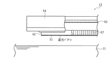
図7は本発明の第1の実施の形態における画像形成装置に使用されるLEDプリントヘッドの構造を示す図、図8は本発明の第1の実施の形態における遮光部材の遮光パターンの構成を示す図である。 FIG. 7 is a diagram showing the structure of the LED print head used in the image forming apparatus according to the first embodiment of the present invention. FIG. 8 is a diagram showing the configuration of the light shielding pattern of the light shielding member according to the first embodiment of the present invention. FIG.
図7に示されるように、露光装置としてのLEDプリントヘッド13は、光源としてのLEDアレイ53及びレンズアレイ52を有する。ここで、前記LEDアレイ53は、レンズホルダ54の天板54aに支持されている基板56の下面に配設され、配列された複数のLED素子を備える。なお、前記基板56には、LED素子の発光を制御するドライバIC等も配設されている。
As shown in FIG. 7, the
また、前記レンズアレイ52は、複数のレンズ素子57と遮光部材51とを備え、LEDアレイ53の下方において、レンズホルダ54に取り付けられている。前記遮光部材51は光源の光を遮光する黒色塗料等による遮光パターンである。なお、前記レンズアレイ52は、図8に示されるように、複数のレンズ素子57と、該レンズ素子57間の間隙を埋める充填材59と、レンズ素子57を固定する当て板58とを有する。
The
次に、前記遮光部材51の遮光パターンの構成について説明する。
Next, the configuration of the light shielding pattern of the
本実施の形態において、遮光部材51の遮光パターンは、レンズ素子57の外周部の一部をLEDアレイ53上のLED素子からの光線を遮光するように形成される。この場合、前記遮光パターンは、図8(a)に示されるように、倒れ具合の比較的良好なレンズ素子57に対し同一の開口径の遮光パターンを形成し、かつ、倒れの比較的大きい倒れ不良のレンズ素子57aに対しては開口径の小さい遮光パターンを形成する。また、倒れ不良のレンズ素子57aに対しては、その倒れの値が大きいほど遮光パターンの開口径を小さくする。すなわち、レンズ素子57による結像位置のずれ量が大きいほど、そのレンズ素子57からの光線を透過する開口部を小さくするようになっている。
In the present embodiment, the light shielding pattern of the
また、図8(b)に示されるように、倒れの比較的大きい倒れ不良のレンズ素子57aに対してのみ遮光パターンを形成してもよい。さらに、倒れの値が大きいほど遮光パターンの開口径を小さくしてもよい。画像形成装置10の解像度が比較的小さい場合、このような遮光パターンの形成方法でも、十分効果が発揮される。
Further, as shown in FIG. 8B, a light-shielding pattern may be formed only for the
また、図8(c)に示されるように、同一の開口径の遮光パターンを形成してもよい。この場合、レンズ素子57の外周部が的確に遮光されるように、遮光パターンの位置をレンズ素子57の位置に合わせる。レンズアレイ52中のレンズ素子57の倒れ不良が比較的小さく良好な場合、このような遮光パターンの形成方法で十分効果が発揮される。
Further, as shown in FIG. 8C, a light shielding pattern having the same opening diameter may be formed. In this case, the position of the light shielding pattern is adjusted to the position of the
本実施の形態においては、図7に示されるように、レンズアレイ52の感光体11側の開口面に遮光部材51を配設しているが、該遮光部材51を配設する場所はレンズアレイ52の感光体11側の開口面に限定されるものではなく、例えば、LEDアレイ53側のレンズアレイ52の開口面に遮光部材51を配設してもよい。
In the present embodiment, as shown in FIG. 7, the
また、本実施の形態における遮光部材51は、図8に示されるように、レンズアレイ52に黒色塗料を用いて直接描画したものであるが、前記遮光部材51の構成はこの限りでなく、光源の光を透過する透明部材に遮光パターンを形成したものであってもよいし、エッチング加工や型成形法によって光源の光を遮光する板材に穴を穿(うが)って開口を形成したものであってもよい。
Further, as shown in FIG. 8, the
さらに、本実施の形態における遮光部材51の遮光パターンは、図8に示されるように、各レンズ素子57の外周部を遮光する円形のパターンであるが、前記遮光パターンの形状は、この限りではなく楕(だ)円形や矩(く)形等でも同様の効果が得られる。また、倒れ不良のレンズ素子57aを完全に遮光しても同様の効果が得られる。
Furthermore, as shown in FIG. 8, the light shielding pattern of the
さらに、本実施の形態における露光装置は、図7に示されるように、光源にLED素子を複数並列したLEDアレイ53を使用したものであるが、前記露光装置の構成はこの限りではなく、例えば、画像形成装置10の露光装置として一般に用いられている半導体レーザや蛍光灯、ハロゲンランプ等の露光源に液晶素子で構成されたシャッタを併用した露光装置であってもよい。
Further, as shown in FIG. 7, the exposure apparatus in the present embodiment uses an
さらに、本実施の形態におけるレンズアレイ52のレンズ素子57は、図7及び8に示されるように、円筒形状であり、中心軸から半径方向に屈折率分布を有するロッドレンズであるが、前記レンズ素子57は、この限りではなく、断面形状が楕円形や矩形のものであってもよい。また、複数の球面レンズや非球面レンズを並列したレンズアレイ52を複数対向するように配置したレンズアレイ52を用いることもできる。
Further, as shown in FIGS. 7 and 8, the
次に、前記遮光部材51の製造方法について説明する。
Next, a method for manufacturing the
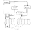
図1は本発明の第1の実施の形態における遮光パターン形成装置の構成を示す図、図9は本発明の第1の実施の形態における光軸傾き測定機の構成と測定原理を示す図、図10は本発明の第1の実施の形態における光量ばらつき測定機の構成を示す図である。 FIG. 1 is a diagram showing a configuration of a light-shielding pattern forming apparatus according to a first embodiment of the present invention, and FIG. 9 is a diagram showing a configuration and measurement principle of an optical axis tilt measuring machine according to the first embodiment of the present invention. FIG. 10 is a diagram showing a configuration of a light quantity variation measuring machine according to the first embodiment of the present invention.
ここで、遮光パターン形成装置は、図1に示されるように、露光装置としてのLEDプリントヘッド13に用いるレンズアレイ52におけるレンズ素子57の中心位置及び光軸の傾きを測定する光軸傾き測定機70、遮光部材51の遮光パターンを形成するインクジェット印刷装置61、該インクジェット印刷装置61を搬送する搬送装置62、前記インクジェット印刷装置61及び搬送装置62を制御する制御装置63、前記光軸傾き測定機70を搬送する図示されない搬送装置、前記光軸傾き測定機70を制御する制御装置65及び記憶装置64から成る。そして、レンズアレイ52を固定し、該レンズアレイ52に対して光軸傾き測定機70を走査して各レンズ素子57の傾きを測定し、その測定データに対応させて、インクジェット印刷装置61を走査させて各レンズ素子57の外周部に遮光部材51を印刷する。
Here, as shown in FIG. 1, the light-shielding pattern forming apparatus is an optical axis inclination measuring device that measures the center position of the
まず、光軸傾き測定機70のCCD(Charge Coupled Device:電荷結合素子)カメラ71を用いて、レンズアレイ52におけるレンズ素子57の中心位置を計測する。光軸傾き測定機70は、図9(a)に示されるように、図示されない搬送装置によってレンズ素子57の配列方向に移動しながら、CCDカメラ71により画像を取り込む。この場合、得られた画像から、図9(b)に示されるようなレンズアレイ52におけるCCDカメラ71に対向する二次元平面における座標を記録するようになっている。すなわち、画像処理装置72は、CCDカメラ71によって得られた図9(b)に示されるような画像から、各レンズ素子57の中心位置77aを割り出し、二次元平面における所定位置を原点(0、0)とし、各レンズ素子57の中心位置77aを(xi、yi)座標として、記憶装置64に格納して記録する。
First, the center position of the
次に、前記光軸傾き測定機70を用いてレンズ素子57の光軸の傾きを測定する。ここで、前記光軸傾き測定機70は、光源76、集光素子75及びCCDカメラ71を有する。前記集光素子75は、光学レンズ等を組み合わせて構成された、光源76からの光線を発光点78に集光するための光学素子である。また、光軸傾き測定機70は、記憶装置64に記録されたレンズアレイ52におけるレンズ素子57の位置データに基づいて、図示されない搬送装置によって搬送される。ここで、測定を行うレンズ素子57に光軸の傾きがなく、理想的に配置されていると仮定した場合に、発光点78と、該発光点78のレンズ素子57による露光像の結像面74上の位置である結像点77とが、レンズ素子57の光軸上に来るように、前記光源76、集光素子75及びCCDカメラ71の配置が決定されている。
Next, the inclination of the optical axis of the
本実施の形態のレンズアレイ52のように、レンズ素子57が二列に並んでいる場合、光軸傾き測定機70を往復移動させる。そして、往路及び復路の各々において、レンズ素子57の各列の略中心線を通るように光軸傾き測定機70を移動させつつ、各列に含まれるレンズ素子57毎に測定を行う。あるいは、単純に千鳥状に位置をずらしながら測定してもよい。
When the
ここで、前記光軸傾き測定機70の光源76を発光すると、結像点77は、レンズ素子57によって、結像面74上に露光される。前記結像点77の結像面74上の位置はレンズ素子57の光軸の傾きによって異なるから、CCDカメラ71によって取り込まれた画像を画像処理装置72によって処理することにより、レンズ素子57の光軸の傾きを計測することができる。先に計測して、記憶装置64に記録された各レンズ素子57の中心位置と、結像点77とを比較することによってずれ量を計測することができる。
Here, when the
そして、前記光軸傾き測定機70は、レンズアレイ52のすべてのレンズ素子57について、図9(b)に示されるように、結像点77のレンズ素子57の中心位置77aに対するx軸方向(レンズアレイ52のレンズ素子57の配列方向)のずれPxを計測し、記憶装置64に格納して記録する。ここで、前記Pxは、レンズ素子57の結像特性としての結像位置ずれの大きさを示している。
Then, as shown in FIG. 9B, the optical axis
この場合、各レンズ素子57の中心位置77aのx座標値と、結像点のx座標値との差から、前記ずれPxを計測することができる。なお、x方向のずれのみを計測する理由は、レンズの配列方向であるx軸方向におけるMTFの低下が主として画像品質の低下を招き、x方向の濃度ムラの発生の原因となるためである。
In this case, the deviation Px can be measured from the difference between the x-coordinate value of the
次に、図1に示されるようなインクジェット印刷装置61を用いて、レンズアレイ52に遮光パターンを形成する。この場合、記憶装置64に記録されたレンズアレイ52におけるレンズ素子57の中心位置77aの位置データとレンズ素子57の傾きデータとに基づいて、遮光パターンを形成する位置を決定し、さらに、傾きデータに基づいて遮光パターンの開口径や形状を決定する。そして、制御装置63によって搬送装置62を制御してインクジェット印刷装置61を搬送し走査させる、制御装置63によってインクジェット印刷装置61を制御して遮光パターンを形成する。
Next, a light shielding pattern is formed on the
なお、該遮光パターンを形成する方法は、インクジェット方式を用いた印刷方法に限定されるものではなく、ペンレコーダや熱転写方式を用いた印刷方法、電子写真方式を用いた印刷方法、インパクト・ドット方式を用いた印刷方法等であってもよい。 The method for forming the light shielding pattern is not limited to the printing method using the ink jet method, the printing method using the pen recorder or the thermal transfer method, the printing method using the electrophotographic method, and the impact dot method. Or a printing method using.
この場合、遮光部材51を形成したレンズアレイ52をLEDアレイ53等とともに組み立てて、図7に示されるような露光装置としてのLEDプリントヘッド13を構成した後、LEDアレイ53中の各発光点の露光量補正を行う。このとき、以下に示す方法で、各LED発光素子の露光像の光量ばらつきを計測し、そのデータをもとにLEDアレイ53の各LED発光素子を動作させ、発光時間を制御することで露光量補正を行う。なお、露光量は、光量と時間との積である。すなわち、露光量=光量×時間である。
In this case, the
次に、図10に示されるような光量ばらつき測定機80によって、露光装置のLED発光素子の露光像の光量ばらつきを測定する。前記光量ばらつき測定機80は、CCDカメラ81、露光装置の発光点の露光像をCCDカメラ81に取り込む集光素子82、CCDカメラ81及び集光素子82を露光装置の発光点の配列方向に搬送し走査させる搬送装置83、CCDカメラ81の画像を画像処理して各発光点の光量ばらつきを計測する画像処理装置86、測定結果を記録する記憶装置85、それらを制御する制御装置84、並びに、測定対象である露光装置としてのLEDプリントヘッド13を動作させる図示されない制御装置を有する。
Next, the light amount variation of the exposure image of the LED light emitting element of the exposure apparatus is measured by a light amount
この場合、LEDプリントヘッド13、CCDカメラ81及び集光素子82は、LEDプリントヘッド13の発光点の露光像にCCDカメラ81の焦点が合うように配置される。また、CCDカメラ81及び集光素子82によってLEDプリントヘッド13の各発光点を走査することができるように、搬送装置83を配置する。
In this case, the
LED発光素子の露光像の光量ばらつき測定においては、まず、LEDプリントヘッド13の各発光点を発光させる。そして、CCDカメラ81により各発光点の露光像の画像を取り込みながら、搬送装置83によってCCDカメラ81及び集光素子82を発光点の配列方向に走査する。CCDカメラ81によって取り込んだ各発光点の露光像の画像は、CCDカメラ81の走査位置データとともに画像処理装置86によって処理され、LEDプリントヘッド13の各発光点についての光量が計測される。なお、計測されたデータは個々のLEDプリントヘッド13を特定するシリアルナンバとともに記憶装置85に記憶される。
In measuring the variation in the amount of light of the exposure image of the LED light emitting element, first, each light emitting point of the
また、個々のLEDプリントヘッド13とその発光点の光量ばらつきを補正するためのLEDプリントヘッド13の各発光点の制御データは、そのLEDプリントヘッド13が取り付けられる画像形成装置10本体の記憶部42に記憶される。そして、個々のLEDプリントヘッド13を特定するシリアルナンバとともに各発光点の制御データを図示されないネットワークに接続されたサーバに記憶しておき、画像形成装置10本体を組み立てる際に前記ネットワークに接続し、組み込んだLEDプリントヘッド13のシリアルナンバから各発光点の制御データ、すなわち、各発光点に対応する露光時間を決定するデータをサーバから呼び出し、画像形成装置10本体の記憶部42に取り込んで記憶する。これにより、画像形成装置10は、組み込まれたLEDプリントヘッド13に対応する各発光点の制御データに従って各発光点の発光時間を制御することができ、各発光部はほぼ均一な発光量を露光することができる。
Further, the control data of each light emitting point of the
前述された光量補正の方法は、各LED発光素子を動作する電流量を調整することで、各LED発光素子の露光像の光量を均一にしてもよい。 In the light amount correction method described above, the amount of light of the exposure image of each LED light emitting element may be made uniform by adjusting the amount of current that operates each LED light emitting element.
なお、個々のLEDプリントヘッド13とその発光点の光量ばらつきを補正するためのLEDプリントヘッド13の各発光点の制御データを、そのLEDプリントヘッド13が取り付けられる画像形成装置10本体の記憶部42に記憶する方法は、前述された方法に限定されるものではない。
Note that the control data of each light emitting point of the
また、個々のLEDプリントヘッド13とその発光点の光量ばらつきを補正するためのLEDプリントヘッド13の各発光点の制御データは、そのLEDプリントヘッド13中に記憶装置を配設して記憶することもできる。
In addition, the control data of each light emitting point of the
次に、前記構成のLEDプリントヘッド13の動作について説明する。
Next, the operation of the
まず、画像形成装置10本体の記憶部42に記憶された、露光像の光量ばらつきを補正するLED発光素子の制御データに基づいて、図7に示される基板56上に配置された図示されないドライバICによってLEDアレイ53が駆動される。すると、該LEDアレイ53が発光して、該LEDアレイ53から発せられた光がレンズアレイ52に入射する。この場合、前記LEDアレイ53から発せられた光のうち、レンズアレイ52のレンズ素子57の外周部付近の光の一部が、図8に示されるような遮光部材51の遮光パターンに当たり遮られる。一方、レンズアレイ52のレンズ素子57を通過した光の一部は、遮光部材51の開口部を通過して、LEDアレイ53の発光した発光点の像が図7に示されるような感光体11上に結像し、該感光体11上に露光像を形成する。
First, a driver IC (not shown) disposed on the
なお、図8に示されるように、レンズアレイ52中で光軸の傾きが比較的大きい倒れ不良のレンズ素子57aにおいては、遮光部材51の遮光パターンの開口径がより小さくなっており、倒れ不良のレンズ素子57aの外周部付近の遮光パターンに当たり遮られる部分は比較的多く、開口部を通過する光は倒れ不良のレンズ素子57aの中心部を透過した光に限られる。
As shown in FIG. 8, in the
また、レンズ素子57の光軸の傾きによって、遮光部材51の遮光パターンの開口径が異なるので、LED発光素子の露光像について単位時間当りの光量にはばらつきが発生する。しかし、前述のように、画像形成装置10の制御部41が画像形成装置10全体の動作に関する制御を行い、LEDヘッド駆動制御部44は、前記制御部41に従って、記憶部42に格納された補正データに基づきLEDプリントヘッド13を駆動する。これにより、画像形成装置10の記憶部42に記憶された露光像の光量ばらつきを補正するLED発光素子の制御データに基づいて、発光点の発光時間が制御されるので、感光体11に照射される露光像の光量は均一となる。
Further, since the opening diameter of the light shielding pattern of the
このように、本実施の形態においては、遮光部材51の遮光パターンにおける開口の中心位置とレンズアレイ52の各レンズ素子57の中心位置77aのずれがないので、各レンズ素子57の外周部の光線のみを的確に遮光することができ、レンズ素子57による結像特性としてのMTFを向上させるという遮光部材51を配設することによる効果を十分に得ることができる。さらに、画像に筋や濃度ムラ等の不具合が発生することもなく良好な画像を得ることができる。そのため、「背景技術」の項で説明した従来の露光装置における遮光部材を設置することによる効果が得られない、レンズ素子の中心付近が遮光されて露光量が大きく減少するので画像に周期的な白筋が発生し、また、感光体上に全く露光像が形成されず、画像形成そのものができなくなる等の問題点を解消することができる。
Thus, in the present embodiment, there is no deviation between the center position of the opening in the light shielding pattern of the
また、光軸の傾きが大きい倒れ不良のレンズ素子57aに対しては、より開口径の小さい遮光パターンを形成するようになっている。すなわち、レンズ素子57による結像特性としての結像位置ずれに応じて遮光部材51の形状又は位置が設定されている。なお、遮光部材51の遮光パターンは、レンズ素子57による結像位置のずれ量が大きいほど、そのレンズ素子57からの光線を透過する開口部が小さいようになっている。そのため、光軸の傾きが大きい倒れ不良のレンズ素子57aからの露光像の被写界深度を大きくし、より鮮明な露光像を形成することができる。これにより、倒れの発生している倒れ不良のレンズ素子57a近辺の露光像のMTF低下を抑え、印刷画像上では縦筋等の画像不良が発生しないようにすることができる。
In addition, a light-shielding pattern having a smaller aperture diameter is formed for the
さらに、レンズ素子57の光軸の傾きによって遮光部材51の遮光パターンの開口径が異なるので、LED光素子の露光像について単位時間当りの光量にはばらつきが発生するが、画像形成装置10本体の記憶部42に記憶された露光像の光量ばらつきを補正するLED発光素子の制御データに基づいて、発光点の発光時間を制御するようになっている。そのため、感光体11に照射される露光像の光量は均一となり、濃度ムラや筋のない、極めて高品位な画像を得ることができる。
Further, since the aperture diameter of the light shielding pattern of the
次に、本発明の第2の実施の形態について説明する。なお、第1の実施の形態と同じ構成を有するものは、同じ符号を付与することによってその説明を省略する。また、前記第1の実施の形態と同じ動作及び同じ効果についても、その説明を省略する。 Next, a second embodiment of the present invention will be described. In addition, what has the same structure as 1st Embodiment attaches the same code | symbol, and abbreviate | omits the description. The description of the same operation and the same effect as those of the first embodiment is also omitted.
図11は本発明の第2の実施の形態における遮光部材の遮光パターンの構成を示す図である。 FIG. 11 is a diagram showing the configuration of the light shielding pattern of the light shielding member in the second embodiment of the present invention.
本実施の形態において、遮光部材51は、光源の光を遮光する黒色塗料等から成り、遮光パターンを形成する。前記遮光部材51の遮光パターンは、レンズ素子57の外周部の一部をLEDアレイ53上のLED素子からの光線を遮光するように形成される。図11(a)に示されるように、レンズ素子57による結像特性としてのMTFの比較的良好なレンズ素子57に対しては、同一の開口径の遮光パターンを形成し、また、MTFの比較的小さいMTF不良のレンズ素子57cに対しては、開口径の小さい遮光パターンを形成する。また、MTF不良のレンズ素子57cに対しては、MTFの値が大きいほど遮光パターンの開口径を小さくする。
In the present embodiment, the
また、図11(b)に示されるように、MTFの比較的小さいMTF不良のレンズ素子57cに対してのみ遮光パターンを形成してもよい。さらに、MTFの値が小さいほど遮光パターンの開口径を小さくしてもよい。露光装置としてのLEDプリントヘッド13を使用する画像形成装置10の解像度が比較的小さい場合、この遮光パターンの形成方法で十分効果が発揮される。
Further, as shown in FIG. 11B, a light shielding pattern may be formed only for the
なお、前記遮光部材51は、図11に示されるように、レンズアレイ52に黒色塗料を用いて直接描画した遮光部材であるが、前記遮光部材51の構成は、この限りでなく、光源の光を透過する透明部材に遮光パターンを形成したものや、エッチング加工又は型成形法によって光源の光を遮光する板材に穴を穿って開口を形成したものであってもよい。
As shown in FIG. 11, the
また、本実施の形態において、遮光部材51の遮光パターンは、図11に示されるように、各レンズ素子57の外周部を遮光する円形のパターンであるが、前記遮光パターンは、この限りではなく、楕円形や矩形等であっても同様の効果を得ることができる。また、MTF不良のレンズ素子57cを完全に遮光しても同様の効果を得ることができる。
In the present embodiment, as shown in FIG. 11, the light shielding pattern of the
さらに、本実施の形態における露光装置は、前記第1の実施の形態と同様に、図7に示されるような光源にLED素子を複数並列したLEDアレイ53を使用したものであるが、前記露光装置の構成はこの限りではなく、例えば、画像形成装置10の露光装置として一般に用いられている半導体レーザや蛍光灯、ハロゲンランプ等の露光源に液晶素子で構成されたシャッタを併用した露光装置であってもよい。
Further, the exposure apparatus according to the present embodiment uses an
さらに、本実施の形態におけるレンズアレイ52のレンズ素子57は、図7及び8に示されるように、円筒形状であり、中心軸から半径方向に屈折率分布を有するロッドレンズであるが、前記レンズ素子57は、この限りではなく、断面形状が楕円形や矩形のものであってもよい。また、複数の球面レンズや非球面レンズを並列したレンズアレイ52を複数対向するように配置したレンズアレイ52を用いることもできる。
Further, as shown in FIGS. 7 and 8, the
次に、本実施の形態の遮光部材51の製造方法について説明する。
Next, a method for manufacturing the
図12は本発明の第2の実施の形態における遮光パターン形成装置の構成を示す図である。 FIG. 12 is a diagram showing a configuration of a light shielding pattern forming apparatus according to the second embodiment of the present invention.
ここで、遮光パターン形成装置は、図12に示されるように、露光装置としてのLEDプリントヘッド13に用いるレンズアレイ52におけるレンズ素子57の中心位置及びレンズ素子57のMTFを測定するCCDカメラ98、集光素子99、画像処理装置96、前記CCDカメラ98を搬送する搬送装置97、前記CCDカメラ98及び搬送装置97を制御する制御装置95、遮光部材51の遮光パターンを形成するインクジェット印刷装置91、該インクジェット印刷装置91を搬送する搬送装置92、前記インクジェット印刷装置91及び搬送装置92を制御する制御装置93、LEDプリントヘッド13を搬送する図示されない搬送装置、LEDプリントヘッド13を制御する図示されない制御装置、記憶装置94等から成る。
Here, as shown in FIG. 12, the light-shielding pattern forming apparatus includes a
まず、CCDカメラ98を用いて、レンズ素子57の中心位置及び各発光点の露光像のMTFを計測する。CCDカメラ98、集光素子99、及び、測定対象であるLEDプリントヘッド13は、LEDアレイ発光点のレンズアレイ52による露光像に焦点が合うように配置され、かつ、搬送装置97によってCCDカメラ98をLED発光素子の配列方向に平行に移動しながら、発光点の露光像を走査することができるように配置される。そして、搬送装置97によってCCDカメラ98をLEDアレイ53の発光点の配列方向に移動させながら、前記CCDカメラ98によって画像を取り込む。得られた画像とCCDカメラ98の位置データとに基づいて、画像処理装置96は各レンズ素子57の中心位置と各発光点でのMTFとを算出し、測定したLEDプリントヘッド13を特定するシリアルナンバとともに記憶装置94に格納して記録する。
First, the
ここで、MTFの測定について説明する。MTFは発光点の配列に注目したときの光量のコントラストを示す。そして、MTFの値が100〔%〕であることは、コントラストが最も大きく、露光装置としての解像力があることを示し、MTFの値が小さくなるほど光量のコントラストが小さくなる。この場合、LEDアレイ53の発光点の配列において、隣接する発光点同士の間隔はレンズ素子57の直径よりも小さいものとする。そして、前記発光点からの光がレンズ素子57を通過して結像する結像面上においては、光量分布が発生する。該光量分布は、各発光点に対応する結像点において光量が最大となり、隣接する結像点の間において光量が最小となるようになっている。ここで、結像面上における光量の最大値をImax とし、最小値をImin とすると、MTFは、ある発光素子に注目したとき、
<MTF>=(Imax −Imin )/(Imax +Imin )×100〔%〕
と定義される。
Here, the measurement of MTF will be described. MTF indicates the contrast of the light amount when attention is paid to the arrangement of the light emitting points. An MTF value of 100 [%] indicates that the contrast is the highest and the resolving power as an exposure apparatus is present. The smaller the MTF value, the smaller the contrast of the light amount. In this case, in the arrangement of the light emitting points of the
<MTF> = (I max −I min ) / (I max + I min ) × 100 [%]
It is defined as
次に、図12に示されるようなインクジェット印刷装置91を用いて、レンズアレイ52に遮光パターンを形成する。この場合、記憶装置94に記録されたレンズアレイ52のレンズ素子57の位置データ及び各発光点のMTF値に基づいて、遮光パターンを形成する位置、遮光パターンの開口径、形状等を決定し、制御装置93によって搬送装置92を制御してインクジェット印刷装置91を搬送し、制御装置93によってインクジェット印刷装置91を制御して遮光パターンを形成する。
Next, a light shielding pattern is formed on the
なお、該遮光パターンを形成する方法は、インクジェット方式を用いた印刷方法に限定されるものではなく、ペンレコーダや熱転写方式を用いた印刷方法、電子写真方式を用いた印刷方法、インパクト・ドット方式を用いた印刷方法等であってもよい。 The method for forming the light shielding pattern is not limited to the printing method using the ink jet method, the printing method using the pen recorder or the thermal transfer method, the printing method using the electrophotographic method, and the impact dot method. Or a printing method using.
次に、LEDアレイ53中の各発光点の光量補正を行う。なお、各LED発光素子の露光像における光量のばらつきは、前記第1の実施の形態と同様に計測される。なお、光量のばらつきを計測するために、図12に示されるようなCCDカメラ98、集光素子99、画像処理装置96等を用いることができる。そして、計測されたデータに基づいてLEDアレイ53の各LED発光素子が動作する発光時間を制御することによって、光量補正を行う。
Next, the light amount correction of each light emitting point in the
そして、前記第1の実施の形態と同様に、個々のLEDプリントヘッド13とその発光点の光量ばらつきを補正するためのLEDプリントヘッド13の各発光点の制御データは、そのLEDプリントヘッド13が取り付けられる画像形成装置10本体の記憶部42に記憶される。
As in the first embodiment, the control data of each light emitting point of the
前述された光量補正の方法は、各LED発光素子を動作する電流量を調整することで、各LED発光素子の露光像の光量を均一にしてもよい。 In the light amount correction method described above, the amount of light of the exposure image of each LED light emitting element may be made uniform by adjusting the amount of current that operates each LED light emitting element.
なお、個々のLEDプリントヘッド13とその発光点の光量ばらつきを補正するためのLEDプリントヘッド13の各発光点の制御データを、そのLEDプリントヘッド13が取り付けられる画像形成装置10本体の記憶部42に記憶する方法は、前述された方法に限定されるものではない。
Note that the control data of each light emitting point of the
また、個々のLEDプリントヘッド13とその発光点の光量ばらつきを補正するためのLEDプリントヘッド13の各発光点の制御データは、そのLEDプリントヘッド13中に記憶装置を配設して記憶することもできる。
In addition, the control data of each light emitting point of the
次に、本実施の形態におけるLEDプリントヘッド13の動作について説明する。
Next, the operation of the
まず、図11(a)に示されるように、レンズアレイ52中のMTFが比較的小さいMTF不良のレンズ素子57cにおいては、遮光パターン51の開口径はより小さくなっている。そのため、MTF不良のレンズ素子57cの外周部付近の遮光パターンに当たって遮られる部分が比較的多く、開口部を通過する光は、MTF不良のレンズ素子57cの中心部を透過した光に限られる。
First, as shown in FIG. 11A, in the
また、各レンズ素子57のMTFの違いによって、遮光パターンの開口径が異なるので、LED発光素子の露光像について単位時間当りの光量にはばらつきが発生するが、画像形成装置10本体の記憶部42に記憶された、露光像の光量ばらつきを補正するLED発光素子の制御データに基づいて発光点の発光時間を制御するので、感光体11に照射される露光像の光量は均一となる。
Further, since the aperture diameter of the light shielding pattern differs depending on the MTF of each
このように、本実施の形態においては、遮光部材51開口の中心位置とレンズアレイ52の各レンズ素子57の中心位置のずれをなくし、各レンズ素子57の外周部の光線のみを的確に遮光することができる。そのため、遮光部材51を配設することによる効果が十分得られるようになった。さらに、画像に筋や濃度ムラ等の不具合が発生することもなく良好な画像が得ることができる。
As described above, in the present embodiment, the deviation between the center position of the opening of the
また、レンズ素子57の材料特性のばらつき、形状ばらつき等のように、前記第1の実施の形態では改善することができなかった、レンズ素子57の倒れ不良以外のばらつきによる不具合を解消することができる。
Further, it is possible to eliminate problems due to variations other than the tilt failure of the
さらに、「背景技術」の項で説明した従来の露光装置においては、MTFが低下しているレンズ素子による露光像は不鮮明となり、印刷画像上では縦筋等の画像不良が発生していたが、本実施の形態においては、MTFが低下しているMTF不良のレンズ素子57cに対してより開口径の小さい遮光パターンを形成することによって、露光像の被写界深度を大きくし、より鮮明な露光像を形成することができるようになっている。すなわち、レンズ素子57による結像特性としてのMTFに応じて前記遮光部材51の形状又は位置が設定されている。なお、遮光部材51の遮光パターンは、レンズ素子57のMTFの値が小さいほど、そのレンズ素子57からの光線を透過する開口部が小さいようになっている。そのため、MTFが低下している近辺での印刷画像上でも縦筋等の画像不良が発生しないようにすることができる。
Furthermore, in the conventional exposure apparatus described in the section of “Background Art”, the exposure image by the lens element having a reduced MTF is unclear, and image defects such as vertical stripes have occurred on the printed image. In the present embodiment, a light shielding pattern having a smaller aperture diameter is formed on the MTF
さらに、レンズ素子57のMTFの値によって、遮光パターンの開口径が異なるので、LED発光素子の露光像について単位時間当りの光量にばらつきが発生するが、画像形成装置10本体の記憶部42に記憶された、露光像の光量ばらつきを補正するLED発光素子の制御データに基づいて、発光点の発光時間を制御するので、感光体11に照射される露光像の光量は均一となり、結果として印刷画像上は濃度ムラや筋のない、極めて高品位な画像を得ることができる。
Further, since the aperture diameter of the light shielding pattern varies depending on the MTF value of the
次に、本発明の第3の実施の形態について説明する。なお、第1及び第2の実施の形態と同じ構成を有するものは、同じ符号を付与することによって、その説明を省略する。また、前記第1及び第2の実施の形態と同じ動作及び同じ効果についても、その説明を省略する。 Next, a third embodiment of the present invention will be described. In addition, what has the same structure as 1st and 2nd embodiment attaches | subjects the same code | symbol, and abbreviate | omits the description. Also, the description of the same operations and effects as those of the first and second embodiments is omitted.
図13は本発明の第3の実施の形態における画像形成装置に使用されるLEDプリントヘッドの構造を示す図である。 FIG. 13 is a diagram showing the structure of an LED print head used in the image forming apparatus according to the third embodiment of the present invention.
ここで、遮光部材51は、光源の光を透過するガラス、樹脂等の部材に光源の光を遮光する黒色塗料等による遮光パターンを形成したものである。前記遮光部材51の遮光パターンは、レンズ素子57の外周部をLEDアレイ53上のLED素子からの光線を遮光するように形成される。そして、遮光パターンは、レンズ素子57の中心(光軸)位置に開口が形成される。
Here, the
また、遮光パターンは、MTFの比較的小さいMTF不良のレンズ素子57cに対して開口径が小さく形成され、MTFの値が小さいほど遮光パターンの開口径が小さくなるように形成される。
The light shielding pattern is formed such that the aperture diameter is smaller with respect to the MTF
本実施の形態においては、光源の光を透過する透明部材に遮光パターンを形成するようになっているが、光源の光を遮光する板材にエッチングや打ち抜き加工を施して開口を形成したり、型成形法によって開口を形成してもよい。 In this embodiment, a light shielding pattern is formed on a transparent member that transmits light from the light source, but an opening is formed by performing etching or punching on a plate material that shields light from the light source. The opening may be formed by a molding method.
また、本実施の形態における遮光部材51の遮光パターンは、各レンズ素子57の外周部を遮光する円形のパターンであるが、前記遮光パターンの形状は、この限りではなく、楕円形や矩形等でも同様の効果が得られる。また、一個又は複数のレンズ素子57全体を覆い光源からの光を遮光するパターンによっても同様の効果が得られる。
In addition, the light shielding pattern of the
さらに、本実施の形態における露光装置は、図13に示されるように、光源にLED素子を複数並列したLEDアレイ53を使用したものであるが、前記露光装置の構成はこの限りではなく、例えば、画像形成装置10の露光装置として一般に用いられている半導体レーザや蛍光灯、ハロゲンランプ等の露光源に液晶素子で構成されたシャッタを併用した露光装置であってもよい。
Further, as shown in FIG. 13, the exposure apparatus in the present embodiment uses an
さらに、本実施の形態におけるレンズアレイ52のレンズ素子57は、図7及び8に示されるように、円筒形状であり、中心軸から半径方向に屈折率分布を有するロッドレンズであるが、前記レンズ素子57は、この限りではなく、断面形状が楕円形や矩形のものであってもよい。また、複数の球面レンズや非球面レンズを並列したレンズアレイ52を複数対向するように配置したレンズアレイ52を用いることもできる。
Further, as shown in FIGS. 7 and 8, the
次に、本実施の形態の遮光部材51の製造方法について説明する。
Next, a method for manufacturing the
図14は本発明の第3の実施の形態における露光装置に用いる遮光部材の製造装置の構成を示す図である。 FIG. 14 is a view showing the arrangement of a light shielding member manufacturing apparatus used in the exposure apparatus according to the third embodiment of the present invention.
ここで、遮光部材51の製造装置は、図14に示されるように、露光装置としてのLEDプリントヘッド13に用いるレンズアレイ52におけるレンズ素子57の中心位置及びレンズ素子57の位置を測定するCCDカメラ119、該CCDカメラ119を搬送する搬送装置118、前記CCDカメラ119及び搬送装置118を制御する制御装置116、画像処理装置117、遮光部材51の遮光パターンを形成する光源111、集光素子112、遮光部材51及びレンズアレイ52を搬送する図示されない搬送装置、前記光源111を搬送する搬送装置113、前記光源111及び搬送装置113を制御する制御装置114、記憶装置115等から成る。なお、遮光部材51とそのパターン形成に用いたレンズアレイ52とは一対一に対応付けがなされ、後工程において、同一のLEDプリントヘッド13として組み立てられる。
Here, as shown in FIG. 14, the manufacturing apparatus of the
まず、CCDカメラ119を用いて、各レンズ素子57の位置を計測する。CCDカメラ119、レンズ素子57、レンズアレイ52等は、搬送装置118によってCCDカメラ119をレンズ素子57の配列方向へ平行に移動しながら、レンズアレイ52上を走査することができるように配置される。そして、搬送装置118によってCCDカメラ119をレンズ素子57の配列方向に移動させながら、CCDカメラ119によって画像を取り込む。得られた画像とCCDカメラ119の位置データとに基づいて、画像処理装置117は、各レンズ素子57の位置を計測し、測定したレンズアレイ52を特定するシリアルナンバとともに記憶装置115に格納して記録する。
First, the position of each
次に、遮光部材51上に遮光パターンを形成する方法について説明する。
Next, a method for forming a light shielding pattern on the
図14に示されるように、集光素子112によって光源111の光が集光される位置とレンズアレイ52の開口面との距離は、レンズアレイ52の焦点距離に等しく、遮光部材51とレンズアレイ52とは並行で、該遮光部材51とレンズアレイ52の開口面との距離は、レンズアレイ52の焦点距離に等しい。そして、光源111及び集光素子112は、搬送装置113によってレンズ素子57の配列方向に並行に搬送され、レンズアレイ52上を走査する。また、光源111はレンズ素子57の中心位置上に到達したときに発光し、光源111からの光は、集光素子112によって集光され、レンズアレイ52によって、遮光部材51上に結像して露光像を形成する。このとき、記憶装置115に記録されたシリアルナンバによって特定される個々のレンズアレイ52におけるレンズ素子57の位置データに基づいて、制御装置114は、搬送装置113を制御して光源111及び集光素子112を搬送するとともに、光源111の発光タイミングを制御する。
As shown in FIG. 14, the distance between the position where the light from the
そして、遮光部材51の遮光パターンの成形方法は、一般に公知のエッチングによる加工方法と同様である。すなわち、遮光部材51上には、あらかじめ感光材料が塗布されている。一方、溶媒は、未感光の感光材料を溶解せず、感光した感光材料は溶解するようになっている。そして、前述のように、レンズアレイ52を透過した光を遮光部材51上に露光して表層に塗布した感光材料を感光させた後、溶媒によって感光した感光材料を溶解し、遮光部材51上にレンズアレイ52を透過した露光像のネガ像を現像する。
The light shielding pattern forming method of the
なお、遮光パターンを成形する方法は、このような方法に限定されるものではなく、遮光部材51上にレンズアレイ52を透過した露光像又は該露光像のネガ像を現像する方法であればいかなる方法であってもよい。
The method for forming the light shielding pattern is not limited to such a method, and any method can be used as long as the exposure image transmitted through the
さらに、遮光パターンが形成された遮光部材51とレンズアレイ52とを露光装置としてのLEDプリントヘッド13に組み込む。なお、LEDプリントヘッド13の構成は図13に示されるようになっている。遮光部材51とレンズアレイ52とをLEDプリントヘッド13に組み込むときの方向は、前述の遮光部材51の遮光パターンを形成する場合の方向と同様であり、図13に示されるように、レンズアレイ52と遮光部材51とを近接して配置する。このとき、該遮光部材51を配置する位置は、レンズアレイ52開口のLEDアレイ53側であってもよい。
Further, the
次に、該LEDアレイ53中の各発光点の光量補正を行う。なお、各LED発光素子の露光像における光量のばらつきの計測は、前記第1の実施の形態と同様に行うので、説明を省略する。
Next, light amount correction of each light emitting point in the
さらに 前記第1の実施の形態と同様に、個々のLEDプリントヘッド13とその発光点の光量ばらつきを補正するためのLEDプリントヘッド13の各発光点の制御データは、そのLEDプリントヘッド13が取り付けられる画像形成装置10本体の記憶部42に記憶される。
Further, as in the first embodiment, the control data of each light emitting point of the
前述された光量補正の方法は、各LED発光素子を動作する電流量を調整することで、各LED発光素子の露光像の光量を均一にしてもよい。 In the light amount correction method described above, the amount of light of the exposure image of each LED light emitting element may be made uniform by adjusting the amount of current that operates each LED light emitting element.
なお、個々のLEDプリントヘッド13とその発光点の光量ばらつきを補正するためのLEDプリントヘッド13の各発光点の制御データを、そのLEDプリントヘッド13が取り付けられる画像形成装置10本体の記憶部42に記憶する方法は、前述された方法に限定されるものではない。
Note that the control data of each light emitting point of the
また、個々のLEDプリントヘッド13とその発光点の光量ばらつきを補正するためのLEDプリントヘッド13の各発光点の制御データは、そのLEDプリントヘッド13中に記憶装置を配設して記憶することもできる。
In addition, the control data of each light emitting point of the
次に、本実施の形態におけるLEDプリントヘッド13の動作について説明する。
Next, the operation of the
前記第2の実施の形態における図11(a)に示される場合と同様に、レンズアレイ52中のMTFが比較的小さいMTF不良のレンズ素子57cにおいては、遮光パターン51の開口径はより小さくなっている。そのため、MTF不良のレンズ素子57cの外周部付近の遮光パターンに当たって遮られる部分が比較的多く、開口部を通過する光は、MTF不良のレンズ素子57cの中心部を透過した光に限られる。
Similarly to the case shown in FIG. 11A in the second embodiment, in the
また、各レンズ素子57のMTFの違いによって、遮光パターンの開口径が異なるので、LED発光素子の露光像について単位時間当りの光量にはばらつきが発生するが、画像形成装置10本体の記憶部42に記憶された、露光像の光量ばらつきを補正するLED発光素子の制御データに基づいて発光点の発光時間を制御するので、感光体11に照射される露光像の光量は均一となる。
Further, since the aperture diameter of the light shielding pattern differs depending on the MTF of each
このように、本実施の形態においては、遮光部材51開口の中心位置とレンズアレイ52の各レンズ素子57の中心位置のずれをなくし、各レンズ素子57の外周部の光線のみを的確に遮光することができる。そのため、遮光部材51を配設することによる効果が十分得られるようになった。さらに、画像に筋や濃度ムラ等の不具合が発生することもなく良好な画像が得ることができる。
As described above, in the present embodiment, the deviation between the center position of the opening of the
また、レンズ素子57の材料特性のばらつきや形状ばらつきによる不具合を解消することができる。
In addition, it is possible to eliminate problems caused by variations in material characteristics and shape variations of the
さらに、「背景技術」の項で説明した従来の露光装置においては、MTFが低下しているレンズ素子による露光像は不鮮明となり、印刷画像上では縦筋等の画像不良が発生していたが、本実施の形態においては、MTFが低下しているMTF不良のレンズ素子57cに対してより開口径の小さい遮光パターンを形成することによって、露光像の被写界深度を大きくし、より鮮明な露光像を形成することができるようになっている。すなわち、レンズ素子57による結像特性としてのMTFに応じて前記遮光部材51の形状又は位置が設定されている。なお、遮光部材51の遮光パターンは、レンズ素子57のMTFの値が小さいほど、そのレンズ素子57からの光線を透過する開口部が小さいようになっている。そのため、MTFが低下している近辺での印刷画像上でも縦筋等の画像不良が発生しないようにすることができる。
Furthermore, in the conventional exposure apparatus described in the section of “Background Art”, the exposure image by the lens element having a reduced MTF is unclear, and image defects such as vertical stripes have occurred on the printed image. In the present embodiment, a light shielding pattern having a smaller aperture diameter is formed on the MTF
さらに、レンズ素子57のMTFの値によって、遮光パターンの開口径が異なるので、LED発光素子の露光像について単位時間当りの光量にばらつきが発生するが、画像形成装置10本体の記憶部42に記憶された、露光像の光量ばらつきを補正するLED発光素子の制御データに基づいて、発光点の発光時間を制御するので、感光体11に照射される露光像の光量は均一となり、結果として印刷画像上は濃度ムラや筋のない、極めて高品位な画像を得ることができる。
Further, since the aperture diameter of the light shielding pattern varies depending on the MTF value of the
さらに、レンズアレイ52やレンズ素子57の特性測定にかかる手間が少なく、レンズ素子57のばらつきによる不具合を解消することができる。
Further, it is less troublesome to measure the characteristics of the
なお、本発明は前記実施の形態に限定されるものではなく、本発明の趣旨に基づいて種々変形させることが可能であり、それらを本発明の範囲から排除するものではない。 In addition, this invention is not limited to the said embodiment, It can change variously based on the meaning of this invention, and does not exclude them from the scope of the present invention.
10 画像形成装置
11 感光体
13 LEDプリントヘッド
51 遮光部材
52 レンズアレイ
53 LEDアレイ
57、57a、57c レンズ素子
76、111 光源
DESCRIPTION OF
Claims (7)
(b)各レンズ素子による結像特性に応じて前記遮光部材の形状又は位置が設定され、
(c)前記結像特性は結像位置ずれであり、前記遮光部材の遮光パターンは、各レンズ素子の結像位置ずれの値に応じて相違し、
(d)前記遮光部材の遮光パターンは、前記レンズ素子の結像位置ずれの値が大きいほど、前記レンズ素子からの光線を透過する開口部であって、前記レンズ素子の外周部を遮光することによって中央に形成される開口部を小さくすることを特徴とする露光装置。 (A) a lens array having a plurality of lens elements for condensing the light from the light source onto the photosensitive member, and a light shielding member for blocking at least a part of the outer periphery of each lens element in the optical axis direction from the light from the light source. And an exposure apparatus used in an electrophotographic image forming apparatus,
(B) The shape or position of the light shielding member is set according to the imaging characteristics of each lens element ,
(C) The imaging characteristic is imaging position deviation, and the light shielding pattern of the light shielding member is different depending on the value of imaging position deviation of each lens element,
(D) The light shielding pattern of the light shielding member is an opening that transmits a light beam from the lens element as the value of the image formation position shift of the lens element increases, and shields the outer periphery of the lens element. exposure apparatus according to claim reduced to Rukoto the opening formed in the center by.
(b)各レンズ素子による結像特性に応じて前記遮光部材の形状又は位置が設定され、(B) The shape or position of the light shielding member is set according to the imaging characteristics of each lens element,
(c)前記結像特性はMTFであり、前記遮光部材の遮光パターンは、各レンズ素子のMTFの値に応じて相違し、(C) The imaging characteristic is MTF, and the light shielding pattern of the light shielding member differs according to the MTF value of each lens element,
(d)前記遮光部材の遮光パターンは、前記レンズ素子のMTFの値が小さいほど、前記レンズ素子からの光線を透過する開口部であって、前記レンズ素子の外周部を遮光することによって中央に形成される開口部を小さくすることを特徴とする露光装置。(D) The light-shielding pattern of the light-shielding member is an opening that transmits light from the lens element as the MTF value of the lens element is smaller, and is centered by shielding the outer periphery of the lens element. An exposure apparatus characterized in that an opening to be formed is made smaller.
(b)各レンズ素子による結像特性に応じて前記遮光部材の形状又は位置が設定され、
(c)前記結像特性は結像位置ずれであり、前記遮光部材の遮光パターンは、各レンズ素子の結像位置ずれの値に応じて相違し、
(d)前記遮光部材の遮光パターンは、前記レンズ素子の結像位置ずれの値が大きいほど、前記レンズ素子からの光線を透過する開口部であって、前記レンズ素子の外周部を遮光することによって中央に形成される開口部を小さくすることを特徴とするLEDプリントヘッド。 (A) a lens array including a plurality of lens elements for condensing the light from the LED array onto the photosensitive member, and a light shielding member for blocking at least a part of the outer peripheral portion of each lens element in the optical axis direction from the light from the LED array An LED print head used in an electrophotographic image forming apparatus,
(B) The shape or position of the light shielding member is set according to the imaging characteristics of each lens element ,
(C) The imaging characteristic is imaging position deviation, and the light shielding pattern of the light shielding member is different depending on the value of imaging position deviation of each lens element,
(D) The light shielding pattern of the light shielding member is an opening that transmits a light beam from the lens element as the value of the image formation position shift of the lens element increases, and shields the outer periphery of the lens element. LED print head, wherein reduced to Rukoto the opening formed in the center by.
(b)各レンズ素子による結像特性に応じて前記遮光部材の形状又は位置が設定され、(B) The shape or position of the light shielding member is set according to the imaging characteristics of each lens element,
(c)前記結像特性はMTFであり、前記遮光部材の遮光パターンは、各レンズ素子のMTFの値に応じて相違し、(C) The imaging characteristic is MTF, and the light shielding pattern of the light shielding member differs according to the MTF value of each lens element,
(d)前記遮光部材の遮光パターンは、前記レンズ素子のMTFの値が小さいほど、前記レンズ素子からの光線を透過する開口部であって、前記レンズ素子の外周部を遮光することによって中央に形成される開口部を小さくすることを特徴とするLEDプリントヘッド。(D) The light-shielding pattern of the light-shielding member is an opening that transmits light from the lens element as the MTF value of the lens element is smaller, and is centered by shielding the outer periphery of the lens element. An LED print head characterized in that an opening formed is made small.
Priority Applications (2)
| Application Number | Priority Date | Filing Date | Title |
|---|---|---|---|
| JP2004192807A JP4416581B2 (en) | 2004-06-30 | 2004-06-30 | Exposure apparatus, LED print head, and image forming apparatus having the same |
| US11/166,079 US7417659B2 (en) | 2004-06-30 | 2005-06-27 | Exposure device, LED print head, and image forming apparatus having the exposure device and the LED print head |
Applications Claiming Priority (1)
| Application Number | Priority Date | Filing Date | Title |
|---|---|---|---|
| JP2004192807A JP4416581B2 (en) | 2004-06-30 | 2004-06-30 | Exposure apparatus, LED print head, and image forming apparatus having the same |
Publications (2)
| Publication Number | Publication Date |
|---|---|
| JP2006015503A JP2006015503A (en) | 2006-01-19 |
| JP4416581B2 true JP4416581B2 (en) | 2010-02-17 |
Family
ID=35513414
Family Applications (1)
| Application Number | Title | Priority Date | Filing Date |
|---|---|---|---|
| JP2004192807A Expired - Fee Related JP4416581B2 (en) | 2004-06-30 | 2004-06-30 | Exposure apparatus, LED print head, and image forming apparatus having the same |
Country Status (2)
| Country | Link |
|---|---|
| US (1) | US7417659B2 (en) |
| JP (1) | JP4416581B2 (en) |
Families Citing this family (11)
| Publication number | Priority date | Publication date | Assignee | Title |
|---|---|---|---|---|
| CA2556533A1 (en) * | 2005-08-24 | 2007-02-24 | Degudent Gmbh | Method of determining the shape of a dental technology object and apparatus performing the method |
| JP4864509B2 (en) * | 2006-03-31 | 2012-02-01 | 株式会社沖データ | Lens array, exposure apparatus, and image forming apparatus |
| EP1952994A3 (en) * | 2007-02-02 | 2009-09-09 | Seiko Epson Corporation | A line head, an exposure method using the line head, and image forming apparatus, an image forming method and a line head adjustment method |
| US7898738B2 (en) * | 2007-09-10 | 2011-03-01 | Oki Data Corporation | Lens array, manufacturing method thereof, LED head having lens array, exposure device having LED head, image forming apparatus having exposure device, and reading apparatus |
| JP4636392B2 (en) * | 2008-06-30 | 2011-02-23 | ブラザー工業株式会社 | Image forming apparatus and manufacturing method thereof |
| JP5267386B2 (en) * | 2009-08-28 | 2013-08-21 | カシオ電子工業株式会社 | Printing apparatus and printing method |
| TWI422946B (en) * | 2009-10-30 | 2014-01-11 | Univ Nat Chiao Tung | Lighting control module, a video camera comprising the same and a control method of the same |
| JP5817764B2 (en) * | 2013-03-13 | 2015-11-18 | コニカミノルタ株式会社 | Optical writing apparatus and image forming apparatus |
| JP6525562B2 (en) * | 2014-11-27 | 2019-06-05 | 株式会社沖データ | Rod lens array, LED print head, contact image sensor head, image forming apparatus, and image reading apparatus |
| JP2017128045A (en) * | 2016-01-20 | 2017-07-27 | 株式会社沖データ | Exposure device, image formation unit, and image formation apparatus |
| US10466501B2 (en) * | 2016-05-26 | 2019-11-05 | Ams Sensors Singapore Pte. Ltd. | Optoelectronic modules including an optical system tilted with respect to a focal plane |
Family Cites Families (9)
| Publication number | Priority date | Publication date | Assignee | Title |
|---|---|---|---|---|
| US4897672A (en) * | 1987-07-02 | 1990-01-30 | Fujitsu Limited | Method and apparatus for detecting and compensating light emission from an LED array |
| US5363240A (en) * | 1992-11-13 | 1994-11-08 | Ricoh Company, Ltd. | Image forming device and method for producing it |
| JP2953684B2 (en) * | 1993-06-25 | 1999-09-27 | 京セラ株式会社 | Imaging device |
| JPH07242018A (en) | 1994-03-02 | 1995-09-19 | Oki Electric Ind Co Ltd | Expose head |
| KR100314425B1 (en) * | 1994-10-05 | 2002-09-19 | 로무 가부시키가이샤 | LED print head |
| US5745152A (en) * | 1994-10-31 | 1998-04-28 | Hewlett Packard Company | Multiple beam laser scanner using lasers with different aperture sizes |
| JP2001255230A (en) * | 2000-03-09 | 2001-09-21 | Nippon Sheet Glass Co Ltd | Evaluation method for image-formation position deviation of lens array |
| JP2001296405A (en) * | 2000-04-12 | 2001-10-26 | Nippon Sheet Glass Co Ltd | Rod lens array |
| TW558518B (en) * | 2001-09-06 | 2003-10-21 | Nippon Sheet Glass Co Ltd | Optical write-in head, image forming apparatus using the same, and method for inspecting the apparatus |
-
2004
- 2004-06-30 JP JP2004192807A patent/JP4416581B2/en not_active Expired - Fee Related
-
2005
- 2005-06-27 US US11/166,079 patent/US7417659B2/en not_active Expired - Fee Related
Also Published As
| Publication number | Publication date |
|---|---|
| US7417659B2 (en) | 2008-08-26 |
| JP2006015503A (en) | 2006-01-19 |
| US20060001733A1 (en) | 2006-01-05 |
Similar Documents
| Publication | Publication Date | Title |
|---|---|---|
| US7417659B2 (en) | Exposure device, LED print head, and image forming apparatus having the exposure device and the LED print head | |
| JP4402674B2 (en) | Lens array, LED head, exposure apparatus and image forming apparatus | |
| JP2008083576A (en) | Lens-array, exposure device, image forming apparatus and reading apparatus | |
| US20070058180A1 (en) | Line Head, Image Forming Apparatus Incorporating the Same, and Method of Adjusting Position of the Same | |
| JP2010164658A (en) | Lens array, lens unit, led head, exposing unit, image forming apparatus, and reading apparatus | |
| JP5584262B2 (en) | Lens unit, LED head, exposure apparatus, image forming apparatus, and reading apparatus | |
| JP2011095627A (en) | Lens unit, led head, exposure device, image forming apparatus, and reading apparatus | |
| JP5222161B2 (en) | Lens unit, LED head, exposure apparatus, image forming apparatus, and reading apparatus | |
| JP2003202516A (en) | Image forming apparatus | |
| JP5061567B2 (en) | Method for adjusting focal position of exposure apparatus | |
| JP5404096B2 (en) | Optical printer head, image forming apparatus, and optical printer head driving method | |
| JP2007147438A (en) | Evaluation method for lens array, evaluator, lens array, and image forming device | |
| CN114488732A (en) | Light emitting device and exposure device | |
| JP2007069399A (en) | Optical head and image forming apparatus having the same | |
| JP4591135B2 (en) | Exposure apparatus and image forming apparatus | |
| JP2022053039A (en) | Light-emitting device and image formation device | |
| JP2022071778A (en) | Light-emitting device, light emitter array chip and exposure apparatus | |
| JP4916069B2 (en) | Imaging element unit, optical writing unit, and image forming apparatus | |
| JP2004098390A (en) | Image forming apparatus | |
| JP2010131802A (en) | Exposure head and image forming apparatus | |
| JP2001322309A (en) | Image-forming apparatus | |
| JP2009151339A (en) | Lens array, exposure device, image forming apparatus and led head | |
| JP2009216730A (en) | Exposure device, image forming apparatus and reading apparatus | |
| JP2006076126A (en) | Adjusting method for print head and image forming apparatus | |
| JP2008012806A (en) | Apparatus and method for forming image |
Legal Events
| Date | Code | Title | Description |
|---|---|---|---|
| A621 | Written request for application examination |
Free format text: JAPANESE INTERMEDIATE CODE: A621 Effective date: 20070223 |
|
| A977 | Report on retrieval |
Free format text: JAPANESE INTERMEDIATE CODE: A971007 Effective date: 20090528 |
|
| A131 | Notification of reasons for refusal |
Free format text: JAPANESE INTERMEDIATE CODE: A131 Effective date: 20090609 |
|
| A521 | Written amendment |
Free format text: JAPANESE INTERMEDIATE CODE: A523 Effective date: 20090810 |
|
| TRDD | Decision of grant or rejection written | ||
| A01 | Written decision to grant a patent or to grant a registration (utility model) |
Free format text: JAPANESE INTERMEDIATE CODE: A01 Effective date: 20091124 |
|
| A01 | Written decision to grant a patent or to grant a registration (utility model) |
Free format text: JAPANESE INTERMEDIATE CODE: A01 |
|
| A61 | First payment of annual fees (during grant procedure) |
Free format text: JAPANESE INTERMEDIATE CODE: A61 Effective date: 20091124 |
|
| R150 | Certificate of patent or registration of utility model |
Free format text: JAPANESE INTERMEDIATE CODE: R150 |
|
| FPAY | Renewal fee payment (event date is renewal date of database) |
Free format text: PAYMENT UNTIL: 20121204 Year of fee payment: 3 |
|
| FPAY | Renewal fee payment (event date is renewal date of database) |
Free format text: PAYMENT UNTIL: 20131204 Year of fee payment: 4 |
|
| LAPS | Cancellation because of no payment of annual fees |