EP0782186B1 - Method to form a buried, implanted plate for DRAM trench storage capacitors - Google Patents
Method to form a buried, implanted plate for DRAM trench storage capacitors Download PDFInfo
- Publication number
- EP0782186B1 EP0782186B1 EP96120100A EP96120100A EP0782186B1 EP 0782186 B1 EP0782186 B1 EP 0782186B1 EP 96120100 A EP96120100 A EP 96120100A EP 96120100 A EP96120100 A EP 96120100A EP 0782186 B1 EP0782186 B1 EP 0782186B1
- Authority
- EP
- European Patent Office
- Prior art keywords
- forming
- wafer
- trench
- layer
- region
- Prior art date
- Legal status (The legal status is an assumption and is not a legal conclusion. Google has not performed a legal analysis and makes no representation as to the accuracy of the status listed.)
- Expired - Lifetime
Links
- 239000003990 capacitor Substances 0.000 title claims description 33
- 238000000034 method Methods 0.000 title claims description 33
- 238000003860 storage Methods 0.000 title claims description 11
- 239000012535 impurity Substances 0.000 claims description 16
- 238000009792 diffusion process Methods 0.000 claims description 15
- 239000004065 semiconductor Substances 0.000 claims description 15
- 238000002955 isolation Methods 0.000 claims description 9
- 239000000463 material Substances 0.000 claims description 5
- 238000009826 distribution Methods 0.000 claims description 4
- OAICVXFJPJFONN-UHFFFAOYSA-N Phosphorus Chemical compound [P] OAICVXFJPJFONN-UHFFFAOYSA-N 0.000 claims description 3
- 229910052698 phosphorus Inorganic materials 0.000 claims description 3
- 239000011574 phosphorus Substances 0.000 claims description 3
- 235000012431 wafers Nutrition 0.000 description 21
- 239000002019 doping agent Substances 0.000 description 19
- 230000015654 memory Effects 0.000 description 19
- 230000008569 process Effects 0.000 description 16
- 238000013461 design Methods 0.000 description 14
- 238000002513 implantation Methods 0.000 description 12
- 239000000758 substrate Substances 0.000 description 11
- 238000005192 partition Methods 0.000 description 9
- 238000000137 annealing Methods 0.000 description 6
- 238000004519 manufacturing process Methods 0.000 description 6
- 230000015572 biosynthetic process Effects 0.000 description 5
- 230000008901 benefit Effects 0.000 description 4
- 238000005530 etching Methods 0.000 description 4
- 238000012545 processing Methods 0.000 description 4
- 238000009825 accumulation Methods 0.000 description 3
- 239000004020 conductor Substances 0.000 description 3
- 230000002093 peripheral effect Effects 0.000 description 3
- 230000009467 reduction Effects 0.000 description 3
- 230000004069 differentiation Effects 0.000 description 2
- 238000005516 engineering process Methods 0.000 description 2
- 230000000873 masking effect Effects 0.000 description 2
- 230000003071 parasitic effect Effects 0.000 description 2
- 230000002829 reductive effect Effects 0.000 description 2
- 230000004308 accommodation Effects 0.000 description 1
- 230000002411 adverse Effects 0.000 description 1
- 230000003466 anti-cipated effect Effects 0.000 description 1
- 238000013459 approach Methods 0.000 description 1
- 230000000903 blocking effect Effects 0.000 description 1
- 230000001808 coupling effect Effects 0.000 description 1
- 230000001419 dependent effect Effects 0.000 description 1
- 238000000151 deposition Methods 0.000 description 1
- 230000008021 deposition Effects 0.000 description 1
- 230000005684 electric field Effects 0.000 description 1
- 230000006870 function Effects 0.000 description 1
- BHEPBYXIRTUNPN-UHFFFAOYSA-N hydridophosphorus(.) (triplet) Chemical compound [PH] BHEPBYXIRTUNPN-UHFFFAOYSA-N 0.000 description 1
- 239000007943 implant Substances 0.000 description 1
- 230000000670 limiting effect Effects 0.000 description 1
- 210000003141 lower extremity Anatomy 0.000 description 1
- 230000007246 mechanism Effects 0.000 description 1
- 238000001465 metallisation Methods 0.000 description 1
- 230000004048 modification Effects 0.000 description 1
- 238000012986 modification Methods 0.000 description 1
- 238000000059 patterning Methods 0.000 description 1
- 229910021420 polycrystalline silicon Inorganic materials 0.000 description 1
- 229920005591 polysilicon Polymers 0.000 description 1
- 230000001105 regulatory effect Effects 0.000 description 1
- 230000008439 repair process Effects 0.000 description 1
- 230000004044 response Effects 0.000 description 1
- 230000003068 static effect Effects 0.000 description 1
Images
Classifications
-
- H—ELECTRICITY
- H10—SEMICONDUCTOR DEVICES; ELECTRIC SOLID-STATE DEVICES NOT OTHERWISE PROVIDED FOR
- H10D—INORGANIC ELECTRIC SEMICONDUCTOR DEVICES
- H10D1/00—Resistors, capacitors or inductors
- H10D1/01—Manufacture or treatment
- H10D1/045—Manufacture or treatment of capacitors having potential barriers, e.g. varactors
- H10D1/047—Manufacture or treatment of capacitors having potential barriers, e.g. varactors of conductor-insulator-semiconductor capacitors, e.g. trench capacitors
-
- H—ELECTRICITY
- H10—SEMICONDUCTOR DEVICES; ELECTRIC SOLID-STATE DEVICES NOT OTHERWISE PROVIDED FOR
- H10B—ELECTRONIC MEMORY DEVICES
- H10B12/00—Dynamic random access memory [DRAM] devices
- H10B12/30—DRAM devices comprising one-transistor - one-capacitor [1T-1C] memory cells
- H10B12/37—DRAM devices comprising one-transistor - one-capacitor [1T-1C] memory cells the capacitor being at least partially in a trench in the substrate
-
- H—ELECTRICITY
- H10—SEMICONDUCTOR DEVICES; ELECTRIC SOLID-STATE DEVICES NOT OTHERWISE PROVIDED FOR
- H10D—INORGANIC ELECTRIC SEMICONDUCTOR DEVICES
- H10D1/00—Resistors, capacitors or inductors
- H10D1/60—Capacitors
- H10D1/62—Capacitors having potential barriers
- H10D1/66—Conductor-insulator-semiconductor capacitors, e.g. MOS capacitors
- H10D1/665—Trench conductor-insulator-semiconductor capacitors, e.g. trench MOS capacitors
Definitions
- the present invention generally relates to integrated circuit memories and, more particularly, to the formation of a plate for trench storage capacitors particularly as used in dynamic random access memories (DRAMs).
- DRAMs dynamic random access memories
- a well-known and widely used capacitor structure occupying an extremely small area on a chip is known as a trench capacitor which, in a basic form includes a capacitor dielectric and an electrode, as one capacitor plate, formed within a blind aperture (often oval in plan view) generally referred to as a trench, in a substrate; using a region within the substrate as the second capacitor plate common to the trench capacitors on the chip.
- the speed with which writing can be done at a given voltage depends, to a large degree, on the parasitic series resistance of the memory cell capacitors. Therefore, it is often desirable to form a structure of enhanced conductivity to serve as a common capacitor plate for the memory cells on a chip or in a partition thereof. Such structures may also facilitate isolation of cells from mutual parasitic coupling effects. As a further refinement, as memory cells have become more densely integrated on a chip, applying a bias to such a conductive structure approximating a voltage mid-way between the logic signal levels allows reduction of electrical field and stress on the capacitor dielectric which can thus be made thinner.
- Some of the read, write and refresh operations as well as differentiation between partitions of memory can be facilitated by biasing the electrode which forms a common capacitor plate for a plurality of capacitors.
- the electrode which forms a common capacitor plate for a plurality of capacitors.
- separate and mutually isolated common electrodes must be provided which, of course, cannot be done if the substrate forms a common electrode for all storage capacitors on the chip.
- the extent of any such electrode must be readily determinable as an incident of chip design in order to avoid interference with other circuitry provided on the chip to allow access to memory cells and to store and recover data, such as address decoders, sense amplifiers and peripheral circuits.
- a separate, independently biasable electrode has been included by a buried doped region within the substrate, such as an n-type region within a p-type substrate and beneath a p-well provided for the capacitor array so that the electrode provided by the buried, doped region will surround the capacitor portion of each trench.
- a buried doped region within the substrate, such as an n-type region within a p-type substrate and beneath a p-well provided for the capacitor array so that the electrode provided by the buried, doped region will surround the capacitor portion of each trench.
- an isolation or other region is formed at the bottom of the trench and some portion of the upper regions of the trench may include transistors or other circuit elements or portions thereof used for accessing a particular capacitor of a memory cell.
- Such buried electrodes have been formed in known DRAM designs, such as that disclosed in U. S. Patent 5,264,716 to Donald M. Kenney and assigned to the assignee of the present invention, by out-diffusion of plate dopant from a diffusion source within the trench, thereby assuring that the doped region so formed will surround the capacitor portion of the trench.
- the process steps required for forming an electrode in this manner involve deposition of the dopant source, masking the vertical dopant profile and removal of the dopant source by etching, These operations involve substantial process complexity and have been found to have a substantial adverse impact on manufacturing yield.
- An alternative method involves the use of an n-type substrate into which a p-type surface implantation is made prior to etching of trenches.
- this approach introduces some additional problems and is subject to some severe operational limitations. Specifically, the low noise and high latch-up resistance of n-well CMOS logic circuitry are sacrificed, a new latch-up mechanism is presented by the necessary p-n-p-n vertical path, the freedom to bias the plate arbitrarily is eliminated, and costs of n-type wafers meeting particular resistivity specifications are substantially higher than for p-type wafers; substantially eliminating the cost benefit of the simpler process. Further, it is not entirely clear at the present state of the art that partitions can be successfully formed consistent with this alternative process.
- US-A-4 794 434 describes a process of manufacturing a buried layer for a trench capacitor wherein an impurity region is formed in the surface of a semiconductor layer. An epitaxial layer is then grown there on before the device is annealed.
- EP-A-0 550 894 describes a similar process of forming a buried capacitor plate for a DRAM.
- a method of forming a buried conductive layer in a semiconductor layer or wafer including the steps of implanting impurities of a first type in a region of a semiconductor layer wafer of a second impurity type to provide a sharply defined distribution peak at a predetermined depth within the semiconductor layer or wafer, forming an epitaxial layer of semiconductor material over a region including implanted impurities of a first type by said implanting step, and diffusing said impurities into said epitaxial layer and said semiconductor layer or wafer to form a diffusion region.
- n-type impurity implantation preferably of phosphorus to a concentration between 10 14 cm -2 and 5 x 10 16 cm -2 or greater at about 900 KeV, is performed in accordance with the mask to form n-type regions 20 as shown in Figure 2.
- n-type impurities may be used for implantation to concentration which develop comparable conductivities in the implanted region.
- phosphorous is preferred, particularly in view of diffusion rates of phosphorus in semiconductor wafer materials.
- any known mask and patterning suitable for implantation can be used.
- the particular masking process used is not important to the practice of the invention and the mask is preferably removed following the implantation.
- the lower impurity concentration is adequate, after diffusion, to support bias conditions resulting in accumulation of the plate. Concentrations approaching or even exceeding the higher concentration would be necessary to additionally support depletion of the plate so that an arbitrary bias can be applied.
- a mask is not necessary except for the purpose of division or articulation of the buried electrode into partitions or limiting the extent of the buried conductor in the vicinity of other circuits of the chip, as may be desired in the memory design, and can be omitted if only a single electrode is to be formed across the entire chip or wafer, common to all capacitors which are later formed.
- an epitaxial p-type layer 30 is then grown over the surface of the wafer; effectively burying the n-type implanted region within the p-type material.
- the thickness of this layer is not particularly critical to the practice of the invention but the thickness should accommodate the formation of transistors above the final n-type region developed by annealing, as will be described below with reference to Figures 4 and 6 while being sufficiently thin to allow connections to be made to the final n-type regions by desired processes, such as a further masked implantation.
- a thickness of approximately 4 ⁇ m is presently preferred as a balance between these considerations in view of preferred forms of trench capacitors to be later formed.
- the buried electrode is then expanded by annealing to spread the n-type implanted impurity downward into the wafer and upward into the epitaxial region by diffusion as well as to repair damage to the crystallographic structure of the wafer resulting from implantation.
- an initial implant of 10 14 /cm 2 at the preferred 900 KeV provides a sharply defined distribution peak at a depth of slightly less than 2 ⁇ m within the original wafer which, after epitaxial growth of 4 ⁇ m as shown in Figure 3, would be depicted at a depth of slightly less than 6 ⁇ m, the approximate center of the dopant concentration peak resulting from a four minute anneal at 1200°C shown by a solid line. As annealing proceeds with time, the center of the dopant concentration profile will remain centered at this location.
- the range of dopant concentrations noted above is set out as an area measure, as is the practice in the art.
- the dopant concentrations depicted in Figure 6 are in volumetric measure and, since the thickness and, hence, volume of material over which the dopant is diffused is very small, the concentrations will appear several orders of magnitude larger. It should be borne in mind that the dopant concentration per unit volume will determine conductivity and whether or not a bias establishing depletion of the region (in addition to accumulation) can be supported and at what depths within the structure.
- the peak concentration is reduced and the peak is widened.
- the valleys such as 62 on either side of the peak which result from counter-doping also widen and deepen somewhat. These valleys are useful in providing isolation and it is therefore preferred that annealing be terminated prior to valley 62' being brought to the surface since it serves to isolate the buried conductor from circuits or devices which are formed at or on the surface of the wafer or substrate.
- isolation at a depth below the surface can be achieved by counter-doping; allowing increased flexibility in developing the final location and depth of valley 64, 64', 64" by continued annealing, if that feature is significant to the design.
- connections to the buried electrode can be made by patterned doping, an etched opening or in any other suitable manner, as generally depicted at 42 of Figure 4, since the bulk of the buried electrode, at any desired dopant concentration possible following the initial implantation, can be brought arbitrarily near the surface as various designs may require.
- the actual dopant concentration varies with depth at respective points along the traces shown in Figure 6 as well as the width (e.g. thickness) of the electrode for a given (e.g. accumulation and/or depletion) mode at a given bias.
- This can be regulated over a wide range by initial implantation concentration as well as annealing temperature and time; the traces of Figure 6 corresponding to the lower extremity of the concentration range disclosed to be preferred, above.
- the dopant concentration which varies with depth in accordance with the invention, provides a relatively well-defined boundary for the buried electrode for any particular bias or conduction mode.
- the invention provides a very flexible methodology for developing electrodes of different dimensions and conduction qualities, as may be required in various designs of DRAMs and other semiconductor integrated circuits since initial dopant concentrations, thickness of epitaxial layer as well as the potential for developing asymmetry of the dopant concentration profile by counter-doping are all variable, at will, to meet the requirements of various designs.
- outline 48 of the buried electrode represents any arbitrary dopant concentration level which will support a desired conductance at that location and bias (which may vary the location of the illustrated boundary somewhat) or the locations of valleys 62', 64' which provide isolation.
- the buried conductor formed in accordance with the invention has been found, in practice, to present relatively well-defined boundaries to or through which trench 46 may readily be formed and will thus define an area within the trench which will function as a capacitor upon formation of a dielectric and a further electrode (which would serve as a memory cell storage node of a DRAM).
- trench 46 fabrication of the remainder of the capacitor structure can proceed in any known manner and in accordance with any design since the remainder of the process is not considered to be critical to the practice of the invention.
- An exemplary trench capacitor structure is shown in Figure 5, including depiction of the original boundary of the implantation region 20 and the final boundary 48 of the buried electrode achieved by diffusion. Trenches 46 terminate within the buried electrode and isolation from the substrate is provided by lower electrode boundaries corresponding to dopant profile valleys 62', 64', respectively.
- a capacitor dielectric 52 is formed, preferably as an oxide-nitride-oxide (ONO) sandwich. Dielectric thickness may be increased or a connector or collar (e.g. 54) formed near the surface of the trench, as desired, and the remainder of the trench filled with polysilicon. Further connections may be formed by metallization or doping 58 which may also form a conduction terminal of a transistor 58, 58' used to access or otherwise control the cell. Such a transistor may also be formed in a well 59 of opposite conductivity type if required by the design so long as the depth of the well remains above the electrode boundary 48 (although for some anticipated bias levels, a connection therebetween could be desirable).
- ONO oxide-nitride-oxide
- the invention provides a low-cost, high yield process for forming a buried electrode which is of substantial flexibility for accommodation of a variety of designs, particularly designs for DRAMs including trench capacitors.
- the invention preserves the benefits of N-well CMOS technology and can be formed on low-cost p-type wafers or substrates while avoiding the process complexity of out-diffusion from dopant diffusion sources deposited in the trenches.
- the electrode formed in accordance with the invention can also support an arbitrary bias or range thereof, as may be required by an integrated circuit design and can be articulated and/or bounded at will, for example, to form memory partitions or accommodate other circuits such as decoders, sense amplifiers and peripheral circuits.
Landscapes
- Semiconductor Memories (AREA)
- Semiconductor Integrated Circuits (AREA)
Description
- The present invention generally relates to integrated circuit memories and, more particularly, to the formation of a plate for trench storage capacitors particularly as used in dynamic random access memories (DRAMs).
- Basic and indispensable operations of digital data processing circuits involve the ability to fetch one or more sequences of digital signal bits from memory, perform an operation thereon and return the result to storage. Therefore, memory structures from which signals can be accessed and to which signals can be stored in a cycle time comparable to an operating cycle of the processing circuit have been required. To answer this requirement random access memories of both static and dynamic types have been developed and their respective designs continually refined over the years.
- Recent advances in digital data processing circuits has greatly increased requirements for large capacity and improved functionality of storage which may be rapidly accessed by the processing circuitry in cycle times which have become extremely short. Dynamic random access memories have generally been used to answer the requirement of increased storage capacity since data is stored therein as charge on a capacitor which can be fabricated at extremely small size and in very large numbers on a single semiconductor chip. A well-known and widely used capacitor structure occupying an extremely small area on a chip is known as a trench capacitor which, in a basic form includes a capacitor dielectric and an electrode, as one capacitor plate, formed within a blind aperture (often oval in plan view) generally referred to as a trench, in a substrate; using a region within the substrate as the second capacitor plate common to the trench capacitors on the chip.
- As is understood by those skilled in the art, storage or retrieval of signals is achieved in modern, high-capacity DRAMs by the storage of very small amounts of charge. Stored charge is also subject to leakage and must be periodically refreshed in order to avoid corruption of data and while the amount of stored charge remains sufficient to provide rapid and reliable response of sense amplifiers, generally by a "read and write back" combination of operations for each cell and which can be performed simultaneously or concurrently in parallel in different partitions of memory.
- The speed with which writing can be done at a given voltage depends, to a large degree, on the parasitic series resistance of the memory cell capacitors. Therefore, it is often desirable to form a structure of enhanced conductivity to serve as a common capacitor plate for the memory cells on a chip or in a partition thereof. Such structures may also facilitate isolation of cells from mutual parasitic coupling effects. As a further refinement, as memory cells have become more densely integrated on a chip, applying a bias to such a conductive structure approximating a voltage mid-way between the logic signal levels allows reduction of electrical field and stress on the capacitor dielectric which can thus be made thinner. Reduction of the dielectric thickness, consistent with the levels of electrical stress which must be tolerated, increases capacitance of each trench capacitor and potential amount of charge storage at a given voltage and allows the "footprint" of each capacitor to be reduced. In view of the number of memory cells which can currently be fabricated on a chip, seemingly slight reductions in cell footprint can provide substantial chip space for further memory cells, so-called peripheral circuits for increased memory functionality and redundant circuits to increase manufacturing yield.
- Some of the read, write and refresh operations as well as differentiation between partitions of memory can be facilitated by biasing the electrode which forms a common capacitor plate for a plurality of capacitors. Particularly as to differentiation between partitions, if partitions are provided, separate and mutually isolated common electrodes must be provided which, of course, cannot be done if the substrate forms a common electrode for all storage capacitors on the chip. Additionally, the extent of any such electrode must be readily determinable as an incident of chip design in order to avoid interference with other circuitry provided on the chip to allow access to memory cells and to store and recover data, such as address decoders, sense amplifiers and peripheral circuits.
- Therefore, in recent DRAM designs, a separate, independently biasable electrode has been included by a buried doped region within the substrate, such as an n-type region within a p-type substrate and beneath a p-well provided for the capacitor array so that the electrode provided by the buried, doped region will surround the capacitor portion of each trench. (Generally an isolation or other region is formed at the bottom of the trench and some portion of the upper regions of the trench may include transistors or other circuit elements or portions thereof used for accessing a particular capacitor of a memory cell.)
- Such buried electrodes have been formed in known DRAM designs, such as that disclosed in U. S. Patent 5,264,716 to Donald M. Kenney and assigned to the assignee of the present invention, by out-diffusion of plate dopant from a diffusion source within the trench, thereby assuring that the doped region so formed will surround the capacitor portion of the trench. However, the process steps required for forming an electrode in this manner involve deposition of the dopant source, masking the vertical dopant profile and removal of the dopant source by etching, These operations involve substantial process complexity and have been found to have a substantial adverse impact on manufacturing yield.
- An alternative method involves the use of an n-type substrate into which a p-type surface implantation is made prior to etching of trenches. However, while avoiding process complexity, this approach introduces some additional problems and is subject to some severe operational limitations. Specifically, the low noise and high latch-up resistance of n-well CMOS logic circuitry are sacrificed, a new latch-up mechanism is presented by the necessary p-n-p-n vertical path, the freedom to bias the plate arbitrarily is eliminated, and costs of n-type wafers meeting particular resistivity specifications are substantially higher than for p-type wafers; substantially eliminating the cost benefit of the simpler process. Further, it is not entirely clear at the present state of the art that partitions can be successfully formed consistent with this alternative process.
- US-A-4 794 434 describes a process of manufacturing a buried layer for a trench capacitor wherein an impurity region is formed in the surface of a semiconductor layer. An epitaxial layer is then grown there on before the device is annealed.
- EP-A-0 550 894 describes a similar process of forming a buried capacitor plate for a DRAM.
- It is therefore an object of the present invention to provide a low-cost, high yield process for forming a buried capacitor electrode compatible with formation of a high capacity DRAM.
- It is another object of the invention to provide a method of plate formation which preserves the benefits of n-well CMOS technology formed on a low-cost p-type wafer, substrate or chip which does not require out-diffusion from an impurity source or other complex process which can compromise manufacturing yield.
- It is a further object of the invention to provide a low cost, high yield process suitable for p-type wafers for forming a buried electrode which can be articulated at will during manufacture and which can be arbitrarily biased in each partition so formed.
- In order to accomplish these and other objects of the invention, a method of forming a buried conductive layer in a semiconductor layer or wafer is provided as set out in claim 1 including the steps of implanting impurities of a first type in a region of a semiconductor layer wafer of a second impurity type to provide a sharply defined distribution peak at a predetermined depth within the semiconductor layer or wafer, forming an epitaxial layer of semiconductor material over a region including implanted impurities of a first type by said implanting step, and diffusing said impurities into said epitaxial layer and said semiconductor layer or wafer to form a diffusion region.
- Further aspects of the invention are set out in the dependent claims.
- The foregoing and other objects, aspects and advantages will be better understood from the following detailed description of a preferred embodiment of the invention with reference to the drawings, in which:
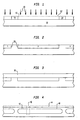
- Figure 1 is a cross-sectional view of a p-type wafer at an initial stage of a preferred implementation of a method in accordance with the invention,
- Figures 2, 3 and 4 are cross sectional views of the wafer at intermediate stages of a preferred form of the method in accordance with the invention,
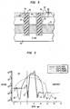
- Figure 5 is a cross-sectional view of a completed capacitor structure formed in accordance with the method of the invention, and
- Figure 6 is a graphical representation of as-found dopant profiles formed in accordance with the invention, as schematically represented in Figure 4.
- Referring now to the drawings, and more particularly to Figure 1, there is shown, in cross-section, a p-
type wafer 10 at an initial stage of the process in accordance with the invention. The wafer is masked, as depicted by dashedline 12 and patterned toopen areas 16 betweenremaining mask areas 14. Then, an n-type impurity implantation, preferably of phosphorus to a concentration between 1014cm-2 and 5 x 1016cm-2 or greater at about 900 KeV, is performed in accordance with the mask to form n-type regions 20 as shown in Figure 2. Some variation in implantation energy may be useful to develop an adequate thickness of the initial impurity concentration distribution in theimplantation region 20. In theory, other n-type impurities may be used for implantation to concentration which develop comparable conductivities in the implanted region. However, phosphorous is preferred, particularly in view of diffusion rates of phosphorus in semiconductor wafer materials. - Any known mask and patterning suitable for implantation can be used. The particular masking process used is not important to the practice of the invention and the mask is preferably removed following the implantation. The lower impurity concentration is adequate, after diffusion, to support bias conditions resulting in accumulation of the plate. Concentrations approaching or even exceeding the higher concentration would be necessary to additionally support depletion of the plate so that an arbitrary bias can be applied. It should also be recognized that a mask is not necessary except for the purpose of division or articulation of the buried electrode into partitions or limiting the extent of the buried conductor in the vicinity of other circuits of the chip, as may be desired in the memory design, and can be omitted if only a single electrode is to be formed across the entire chip or wafer, common to all capacitors which are later formed.
- While not of importance to the practice of the invention, it has been found preferable at this point in the process to again mask the structure with a blocking mask and to pattern openings for etching of alignment marks, if required.
- As shown in Figure 3, an epitaxial p-
type layer 30 is then grown over the surface of the wafer; effectively burying the n-type implanted region within the p-type material. The thickness of this layer is not particularly critical to the practice of the invention but the thickness should accommodate the formation of transistors above the final n-type region developed by annealing, as will be described below with reference to Figures 4 and 6 while being sufficiently thin to allow connections to be made to the final n-type regions by desired processes, such as a further masked implantation. A thickness of approximately 4µm is presently preferred as a balance between these considerations in view of preferred forms of trench capacitors to be later formed. - As shown in Figure 4, the buried electrode is then expanded by annealing to spread the n-type implanted impurity downward into the wafer and upward into the epitaxial region by diffusion as well as to repair damage to the crystallographic structure of the wafer resulting from implantation. Quantitatively, as shown in Figure 6, an initial implant of 1014/cm2 at the preferred 900 KeV provides a sharply defined distribution peak at a depth of slightly less than 2µm within the original wafer which, after epitaxial growth of 4µm as shown in Figure 3, would be depicted at a depth of slightly less than 6µm, the approximate center of the dopant concentration peak resulting from a four minute anneal at 1200°C shown by a solid line. As annealing proceeds with time, the center of the dopant concentration profile will remain centered at this location.
- It should also be noted in consideration of Figure 6 that the range of dopant concentrations noted above is set out as an area measure, as is the practice in the art. The dopant concentrations depicted in Figure 6 are in volumetric measure and, since the thickness and, hence, volume of material over which the dopant is diffused is very small, the concentrations will appear several orders of magnitude larger. It should be borne in mind that the dopant concentration per unit volume will determine conductivity and whether or not a bias establishing depletion of the region (in addition to accumulation) can be supported and at what depths within the structure.
- Accordingly, as diffusion proceeds over time, as shown by the dashed plot corresponding to 60 minutes and the dotted plot corresponding to 120 minutes, the peak concentration is reduced and the peak is widened. It should also be noted that the valleys such as 62 on either side of the peak which result from counter-doping also widen and deepen somewhat. These valleys are useful in providing isolation and it is therefore preferred that annealing be terminated prior to valley 62' being brought to the surface since it serves to isolate the buried conductor from circuits or devices which are formed at or on the surface of the wafer or substrate. However, if the overall doping concentrations are adequately low, such as 1016/ cm3 as shown near the surface in the 120 minute trace, isolation at a depth below the surface can be achieved by counter-doping; allowing increased flexibility in developing the final location and depth of
valley - It should also be understood that the actual dopant concentration varies with depth at respective points along the traces shown in Figure 6 as well as the width (e.g. thickness) of the electrode for a given (e.g. accumulation and/or depletion) mode at a given bias. This can be regulated over a wide range by initial implantation concentration as well as annealing temperature and time; the traces of Figure 6 corresponding to the lower extremity of the concentration range disclosed to be preferred, above. Thus, the dopant concentration, which varies with depth in accordance with the invention, provides a relatively well-defined boundary for the buried electrode for any particular bias or conduction mode. Therefore, the invention provides a very flexible methodology for developing electrodes of different dimensions and conduction qualities, as may be required in various designs of DRAMs and other semiconductor integrated circuits since initial dopant concentrations, thickness of epitaxial layer as well as the potential for developing asymmetry of the dopant concentration profile by counter-doping are all variable, at will, to meet the requirements of various designs.
- Following annealing, as shown in Figure 4, the wafer or substrate is again masked and patterned (e.g. 44) and
trench 46 formed by anisotropic etching; many suitable techniques for which are well-known in the art. In this regard, outline 48 of the buried electrode represents any arbitrary dopant concentration level which will support a desired conductance at that location and bias (which may vary the location of the illustrated boundary somewhat) or the locations of valleys 62', 64' which provide isolation. In any event, the buried conductor formed in accordance with the invention has been found, in practice, to present relatively well-defined boundaries to or through whichtrench 46 may readily be formed and will thus define an area within the trench which will function as a capacitor upon formation of a dielectric and a further electrode (which would serve as a memory cell storage node of a DRAM). - Once
trench 46 is formed, fabrication of the remainder of the capacitor structure can proceed in any known manner and in accordance with any design since the remainder of the process is not considered to be critical to the practice of the invention. An exemplary trench capacitor structure is shown in Figure 5, including depiction of the original boundary of theimplantation region 20 and thefinal boundary 48 of the buried electrode achieved by diffusion.Trenches 46 terminate within the buried electrode and isolation from the substrate is provided by lower electrode boundaries corresponding to dopant profile valleys 62', 64', respectively. - Within the
trenches 46, acapacitor dielectric 52 is formed, preferably as an oxide-nitride-oxide (ONO) sandwich. Dielectric thickness may be increased or a connector or collar (e.g. 54) formed near the surface of the trench, as desired, and the remainder of the trench filled with polysilicon. Further connections may be formed by metallization ordoping 58 which may also form a conduction terminal of atransistor 58, 58' used to access or otherwise control the cell. Such a transistor may also be formed in a well 59 of opposite conductivity type if required by the design so long as the depth of the well remains above the electrode boundary 48 (although for some anticipated bias levels, a connection therebetween could be desirable). - In view of the foregoing, it is seen that the invention provides a low-cost, high yield process for forming a buried electrode which is of substantial flexibility for accommodation of a variety of designs, particularly designs for DRAMs including trench capacitors. The invention preserves the benefits of N-well CMOS technology and can be formed on low-cost p-type wafers or substrates while avoiding the process complexity of out-diffusion from dopant diffusion sources deposited in the trenches. The electrode formed in accordance with the invention can also support an arbitrary bias or range thereof, as may be required by an integrated circuit design and can be articulated and/or bounded at will, for example, to form memory partitions or accommodate other circuits such as decoders, sense amplifiers and peripheral circuits.
- While the invention has been described in terms of a single preferred embodiment, those skilled in the art will recognize that the invention can be practiced with modification within the scope of the appended claims.
Claims (6)
- A method of forming a buried conductive layer in a semiconductor layer or wafer including the steps of
implanting impurities of a first conductivity type in a region of the semiconductor layer or wafer of a second impurity conductivity type to provide a sharply defined distribution peak at a predetermined depth below the surface of the semiconductor layer or wafer,
forming an epitaxial layer of semiconductor material over the region including impurities of said first type implanted by said implanting step, and
diffusing said impurities implanted by said implanting step into said epitaxial layer and said semiconductor layer or wafer to form a diffusion region. - A method as recited in claim 1, wherein in the implanting step n-type impurities, preferably phosphorus, are implanted in a concentration between 1014 cm-2 and 5 x 1016 cm-2.
- A method as recited in claim 1, wherein a thickness of said epitaxial layer formed by said growing step is approximately 4 µm.
- A method as recited in claim 1, wherein said diffusion step further includes the step of
terminating said diffusion step to maintain an isolation region within said epitaxial layer. - A method as recited in claim 1, including the further step of
forming an isolation region within said epitaxial layer by counter-doping. - A method of forming a trench capacitor including the steps of
forming a buried conductive layer in a semiconductor layer or wafer by a method according to any of claims 1 to 5,
forming a trench extending at least to said symmetric diffusion region within said epitaxial layer,
forming a dielectric layer within said trench, and
forming a storage node within said dielectric layer within said trench.
Applications Claiming Priority (2)
| Application Number | Priority Date | Filing Date | Title |
|---|---|---|---|
| US580816 | 1995-12-27 | ||
| US08/580,816 US5908310A (en) | 1995-12-27 | 1995-12-27 | Method to form a buried implanted plate for DRAM trench storage capacitors |
Publications (3)
| Publication Number | Publication Date |
|---|---|
| EP0782186A2 EP0782186A2 (en) | 1997-07-02 |
| EP0782186A3 EP0782186A3 (en) | 1999-08-04 |
| EP0782186B1 true EP0782186B1 (en) | 2006-06-14 |
Family
ID=24322683
Family Applications (1)
| Application Number | Title | Priority Date | Filing Date |
|---|---|---|---|
| EP96120100A Expired - Lifetime EP0782186B1 (en) | 1995-12-27 | 1996-12-13 | Method to form a buried, implanted plate for DRAM trench storage capacitors |
Country Status (5)
| Country | Link |
|---|---|
| US (2) | US5908310A (en) |
| EP (1) | EP0782186B1 (en) |
| JP (1) | JPH09186301A (en) |
| KR (1) | KR100468310B1 (en) |
| DE (1) | DE69636244T2 (en) |
Families Citing this family (7)
| Publication number | Priority date | Publication date | Assignee | Title |
|---|---|---|---|---|
| US5908310A (en) * | 1995-12-27 | 1999-06-01 | International Business Machines Corporation | Method to form a buried implanted plate for DRAM trench storage capacitors |
| JP3988262B2 (en) * | 1998-07-24 | 2007-10-10 | 富士電機デバイステクノロジー株式会社 | Vertical superjunction semiconductor device and manufacturing method thereof |
| DE19843641A1 (en) | 1998-09-23 | 2000-04-20 | Siemens Ag | Trench capacitor with insulation collar and corresponding manufacturing process |
| KR100510997B1 (en) * | 2000-06-29 | 2005-08-31 | 주식회사 하이닉스반도체 | Method For Forming The Junction Electrode Of Semiconductor Device |
| DE10202139B4 (en) * | 2002-01-21 | 2006-07-13 | Infineon Technologies Ag | Memory cell with a thin insulation collar and memory module |
| KR101099562B1 (en) | 2004-07-21 | 2011-12-28 | 매그나칩 반도체 유한회사 | Method of manufacturing semiconductor device |
| US8557657B1 (en) * | 2012-05-18 | 2013-10-15 | International Business Machines Corporation | Retrograde substrate for deep trench capacitors |
Family Cites Families (34)
| Publication number | Priority date | Publication date | Assignee | Title |
|---|---|---|---|---|
| JPS6072258A (en) * | 1983-09-28 | 1985-04-24 | Matsushita Electric Ind Co Ltd | Formation of well |
| JPS60105265A (en) * | 1983-11-11 | 1985-06-10 | Toshiba Corp | Manufacture of complementary type semiconductor device |
| JPS60152058A (en) * | 1984-01-20 | 1985-08-10 | Toshiba Corp | Semiconductor memory device |
| US4688063A (en) * | 1984-06-29 | 1987-08-18 | International Business Machines Corporation | Dynamic ram cell with MOS trench capacitor in CMOS |
| JPS6224617A (en) * | 1985-07-24 | 1987-02-02 | Sumitomo Electric Ind Ltd | Epitaxial growth method |
| US4829017A (en) * | 1986-09-25 | 1989-05-09 | Texas Instruments Incorporated | Method for lubricating a high capacity dram cell |
| US4801988A (en) * | 1986-10-31 | 1989-01-31 | International Business Machines Corporation | Semiconductor trench capacitor cell with merged isolation and node trench construction |
| DE3851649T2 (en) * | 1987-03-20 | 1995-05-04 | Nippon Electric Co | Dynamic random access memory device composed of a plurality of single transistor cells. |
| JPS63245954A (en) * | 1987-04-01 | 1988-10-13 | Hitachi Ltd | semiconductor memory |
| JPS63246861A (en) * | 1987-04-02 | 1988-10-13 | Toshiba Corp | Semiconductor device |
| US4905065A (en) * | 1987-05-12 | 1990-02-27 | Advanced Micro Devices, Inc. | High density dram trench capacitor isolation employing double epitaxial layers |
| US4794434A (en) * | 1987-07-06 | 1988-12-27 | Motorola, Inc. | Trench cell for a dram |
| DE3855945T2 (en) * | 1987-07-10 | 1997-11-13 | Toshiba Kawasaki Kk | Semiconductor component with areas of different impurity concentration |
| JPS6439057A (en) * | 1987-08-04 | 1989-02-09 | Nec Corp | Semiconductor storage device |
| JPH0797626B2 (en) * | 1987-10-31 | 1995-10-18 | 日本電気株式会社 | MIS type semiconductor memory device |
| JPH01227468A (en) * | 1988-03-08 | 1989-09-11 | Oki Electric Ind Co Ltd | Semiconductor storage device |
| JP2623293B2 (en) * | 1988-05-20 | 1997-06-25 | 日本テキサス・インスツルメンツ株式会社 | Semiconductor integrated circuit device |
| JPH0228367A (en) * | 1988-07-18 | 1990-01-30 | Hitachi Ltd | semiconductor storage device |
| JPH02135776A (en) * | 1988-11-17 | 1990-05-24 | Hitachi Ltd | semiconductor storage device |
| US5006909A (en) * | 1989-10-30 | 1991-04-09 | Motorola, Inc. | Dram with a vertical capacitor and transistor |
| JPH03232266A (en) * | 1990-02-07 | 1991-10-16 | Fujitsu Ltd | Semiconductor device and manufacture thereof |
| US5065273A (en) * | 1990-12-04 | 1991-11-12 | International Business Machines Corporation | High capacity DRAM trench capacitor and methods of fabricating same |
| US5279987A (en) * | 1991-10-31 | 1994-01-18 | International Business Machines Corporation | Fabricating planar complementary patterned subcollectors with silicon epitaxial layer |
| DE69229717T2 (en) * | 1992-01-09 | 2000-03-02 | International Business Machines Corp., Armonk | Trench DRAM cell matrix |
| US5250829A (en) * | 1992-01-09 | 1993-10-05 | International Business Machines Corporation | Double well substrate plate trench DRAM cell array |
| US5264716A (en) * | 1992-01-09 | 1993-11-23 | International Business Machines Corporation | Diffused buried plate trench dram cell array |
| JPH07112049B2 (en) * | 1992-01-09 | 1995-11-29 | インターナショナル・ビジネス・マシーンズ・コーポレイション | Dynamic random access memory device and manufacturing method |
| JPH0637275A (en) * | 1992-07-13 | 1994-02-10 | Toshiba Corp | Semiconductor memory and manufacture thereof |
| JPH06120241A (en) * | 1992-10-06 | 1994-04-28 | Nippon Steel Corp | Method for manufacturing semiconductor device |
| JP3439493B2 (en) * | 1992-12-01 | 2003-08-25 | 沖電気工業株式会社 | Method for manufacturing semiconductor memory device |
| US5363327A (en) * | 1993-01-19 | 1994-11-08 | International Business Machines Corporation | Buried-sidewall-strap two transistor one capacitor trench cell |
| US5405790A (en) * | 1993-11-23 | 1995-04-11 | Motorola, Inc. | Method of forming a semiconductor structure having MOS, bipolar, and varactor devices |
| US5476800A (en) * | 1994-01-31 | 1995-12-19 | Burton; Gregory N. | Method for formation of a buried layer for a semiconductor device |
| US5908310A (en) * | 1995-12-27 | 1999-06-01 | International Business Machines Corporation | Method to form a buried implanted plate for DRAM trench storage capacitors |
-
1995
- 1995-12-27 US US08/580,816 patent/US5908310A/en not_active Expired - Fee Related
-
1996
- 1996-07-15 US US08/679,799 patent/US6180972B1/en not_active Expired - Fee Related
- 1996-12-13 EP EP96120100A patent/EP0782186B1/en not_active Expired - Lifetime
- 1996-12-13 DE DE69636244T patent/DE69636244T2/en not_active Expired - Fee Related
- 1996-12-25 JP JP8345898A patent/JPH09186301A/en active Pending
- 1996-12-27 KR KR1019960073540A patent/KR100468310B1/en not_active Expired - Fee Related
Also Published As
| Publication number | Publication date |
|---|---|
| KR100468310B1 (en) | 2005-04-13 |
| DE69636244D1 (en) | 2006-07-27 |
| KR970053614A (en) | 1997-07-31 |
| JPH09186301A (en) | 1997-07-15 |
| EP0782186A2 (en) | 1997-07-02 |
| US6180972B1 (en) | 2001-01-30 |
| DE69636244T2 (en) | 2007-04-26 |
| EP0782186A3 (en) | 1999-08-04 |
| US5908310A (en) | 1999-06-01 |
Similar Documents
| Publication | Publication Date | Title |
|---|---|---|
| US5300450A (en) | High performance composed pillar DRAM cell | |
| US5106776A (en) | Method of making high performance composed pillar dRAM cell | |
| US5670805A (en) | Controlled recrystallization of buried strap in a semiconductor memory device | |
| US5710072A (en) | Method of producing and arrangement containing self-amplifying dynamic MOS transistor memory cells | |
| US6777280B2 (en) | Method for fabricating an integrated circuit with a transistor electrode | |
| US4225945A (en) | Random access MOS memory cell using double level polysilicon | |
| US4855953A (en) | Semiconductor memory device having stacked memory capacitors and method for manufacturing the same | |
| US5016070A (en) | Stacked CMOS sRAM with vertical transistors and cross-coupled capacitors | |
| US7339220B2 (en) | Memory device with surface-channel peripheral transistors | |
| EP0149799B1 (en) | Semiconductor memory device | |
| EP0167764B1 (en) | Dynamic ram cell | |
| US6091630A (en) | Radiation hardened semiconductor memory | |
| US6004844A (en) | Unit cell layout and transfer gate design for high density DRAMs | |
| KR19990023762A (en) | Gain Cells for Dynamic Random Access Memory and Bismos Dynamic Random Access Memory Manufacturing Method | |
| US6265278B1 (en) | Deep trench cell capacitor with inverting counter electrode | |
| JPH03129769A (en) | Dynamic ram storge element and its manufacture | |
| US5250458A (en) | Method for manufacturing semiconductor memory device having stacked memory capacitors | |
| US5908310A (en) | Method to form a buried implanted plate for DRAM trench storage capacitors | |
| US5932906A (en) | DRAM semiconductor device | |
| US5010379A (en) | Semiconductor memory device with two storage nodes | |
| US4353082A (en) | Buried sense line V-groove MOS random access memory | |
| US5340768A (en) | Method of fabricating self-aligned field-plate isolation between control electrodes | |
| US7163857B2 (en) | Buried strap contact for a storage capacitor and method for fabricating it | |
| US6037203A (en) | Method of fabricating a semiconductor device having triple well structure | |
| KR100319623B1 (en) | Dram cell array and fabrication method thereof |
Legal Events
| Date | Code | Title | Description |
|---|---|---|---|
| PUAI | Public reference made under article 153(3) epc to a published international application that has entered the european phase |
Free format text: ORIGINAL CODE: 0009012 |
|
| AK | Designated contracting states |
Kind code of ref document: A2 Designated state(s): DE FR GB IE IT |
|
| PUAL | Search report despatched |
Free format text: ORIGINAL CODE: 0009013 |
|
| AK | Designated contracting states |
Kind code of ref document: A3 Designated state(s): DE FR GB IE IT |
|
| RIC1 | Information provided on ipc code assigned before grant |
Free format text: 6H 01L 21/8242 A, 6H 01L 27/108 B |
|
| 17P | Request for examination filed |
Effective date: 20000217 |
|
| 17Q | First examination report despatched |
Effective date: 20001130 |
|
| RAP1 | Party data changed (applicant data changed or rights of an application transferred) |
Owner name: INTERNATIONAL BUSINESS MACHINES CORPORATION Owner name: INFINEON TECHNOLOGIES AG |
|
| GRAP | Despatch of communication of intention to grant a patent |
Free format text: ORIGINAL CODE: EPIDOSNIGR1 |
|
| RTI1 | Title (correction) |
Free format text: METHOD TO FORM A BURIED, IMPLANTED PLATE FOR DRAM TRENCH STORAGE CAPACITORS |
|
| GRAS | Grant fee paid |
Free format text: ORIGINAL CODE: EPIDOSNIGR3 |
|
| GRAA | (expected) grant |
Free format text: ORIGINAL CODE: 0009210 |
|
| AK | Designated contracting states |
Kind code of ref document: B1 Designated state(s): DE FR GB IE IT |
|
| REG | Reference to a national code |
Ref country code: GB Ref legal event code: FG4D |
|
| REG | Reference to a national code |
Ref country code: IE Ref legal event code: FG4D |
|
| REF | Corresponds to: |
Ref document number: 69636244 Country of ref document: DE Date of ref document: 20060727 Kind code of ref document: P |
|
| PG25 | Lapsed in a contracting state [announced via postgrant information from national office to epo] |
Ref country code: IE Free format text: LAPSE BECAUSE OF NON-PAYMENT OF DUE FEES Effective date: 20061213 |
|
| PGFP | Annual fee paid to national office [announced via postgrant information from national office to epo] |
Ref country code: GB Payment date: 20061221 Year of fee payment: 11 |
|
| ET | Fr: translation filed | ||
| PLBE | No opposition filed within time limit |
Free format text: ORIGINAL CODE: 0009261 |
|
| STAA | Information on the status of an ep patent application or granted ep patent |
Free format text: STATUS: NO OPPOSITION FILED WITHIN TIME LIMIT |
|
| 26N | No opposition filed |
Effective date: 20070315 |
|
| PGFP | Annual fee paid to national office [announced via postgrant information from national office to epo] |
Ref country code: IT Payment date: 20071221 Year of fee payment: 12 |
|
| PGFP | Annual fee paid to national office [announced via postgrant information from national office to epo] |
Ref country code: DE Payment date: 20080213 Year of fee payment: 12 |
|
| PGFP | Annual fee paid to national office [announced via postgrant information from national office to epo] |
Ref country code: FR Payment date: 20071217 Year of fee payment: 12 |
|
| GBPC | Gb: european patent ceased through non-payment of renewal fee |
Effective date: 20071213 |
|
| PG25 | Lapsed in a contracting state [announced via postgrant information from national office to epo] |
Ref country code: GB Free format text: LAPSE BECAUSE OF NON-PAYMENT OF DUE FEES Effective date: 20071213 |
|
| REG | Reference to a national code |
Ref country code: FR Ref legal event code: ST Effective date: 20090831 |
|
| PG25 | Lapsed in a contracting state [announced via postgrant information from national office to epo] |
Ref country code: DE Free format text: LAPSE BECAUSE OF NON-PAYMENT OF DUE FEES Effective date: 20090701 |
|
| PG25 | Lapsed in a contracting state [announced via postgrant information from national office to epo] |
Ref country code: FR Free format text: LAPSE BECAUSE OF NON-PAYMENT OF DUE FEES Effective date: 20081231 |
|
| PG25 | Lapsed in a contracting state [announced via postgrant information from national office to epo] |
Ref country code: IT Free format text: LAPSE BECAUSE OF NON-PAYMENT OF DUE FEES Effective date: 20081213 |