EP0780971A2 - Leistungsverstärkervortreiberstufe - Google Patents
Leistungsverstärkervortreiberstufe Download PDFInfo
- Publication number
- EP0780971A2 EP0780971A2 EP96402753A EP96402753A EP0780971A2 EP 0780971 A2 EP0780971 A2 EP 0780971A2 EP 96402753 A EP96402753 A EP 96402753A EP 96402753 A EP96402753 A EP 96402753A EP 0780971 A2 EP0780971 A2 EP 0780971A2
- Authority
- EP
- European Patent Office
- Prior art keywords
- transistor
- transistors
- resistor
- coupled
- amplifier circuit
- Prior art date
- Legal status (The legal status is an assumption and is not a legal conclusion. Google has not performed a legal analysis and makes no representation as to the accuracy of the status listed.)
- Granted
Links
- 230000007423 decrease Effects 0.000 description 9
- 230000000295 complement effect Effects 0.000 description 2
- 230000001419 dependent effect Effects 0.000 description 2
- 238000010586 diagram Methods 0.000 description 2
- 239000004065 semiconductor Substances 0.000 description 2
- 241000226585 Antennaria plantaginifolia Species 0.000 description 1
- 239000003086 colorant Substances 0.000 description 1
- 230000001066 destructive effect Effects 0.000 description 1
- 238000004519 manufacturing process Methods 0.000 description 1
- 238000000034 method Methods 0.000 description 1
Images

Classifications
-
- H—ELECTRICITY
- H03—ELECTRONIC CIRCUITRY
- H03F—AMPLIFIERS
- H03F3/00—Amplifiers with only discharge tubes or only semiconductor devices as amplifying elements
- H03F3/20—Power amplifiers, e.g. Class B amplifiers, Class C amplifiers
-
- H—ELECTRICITY
- H03—ELECTRONIC CIRCUITRY
- H03F—AMPLIFIERS
- H03F3/00—Amplifiers with only discharge tubes or only semiconductor devices as amplifying elements
- H03F3/30—Single-ended push-pull [SEPP] amplifiers; Phase-splitters therefor
- H03F3/3069—Single-ended push-pull [SEPP] amplifiers; Phase-splitters therefor the emitters of complementary power transistors being connected to the output
- H03F3/3076—Single-ended push-pull [SEPP] amplifiers; Phase-splitters therefor the emitters of complementary power transistors being connected to the output with symmetrical driving of the end stage
-
- H—ELECTRICITY
- H03—ELECTRONIC CIRCUITRY
- H03F—AMPLIFIERS
- H03F3/00—Amplifiers with only discharge tubes or only semiconductor devices as amplifying elements
- H03F3/30—Single-ended push-pull [SEPP] amplifiers; Phase-splitters therefor
- H03F3/3066—Single-ended push-pull [SEPP] amplifiers; Phase-splitters therefor the collectors of complementary power transistors being connected to the output
Definitions
- This invention relates generally to the field of amplifier circuits, and, in particular, to predriver stages for driving output stages in power amplifiers that drive deflection coils in, for example, convergence yokes of cathode ray tubes.
- Cathode ray tubes (CRTs) used in television receivers are subject to distortions of the video image on the CRT's faceplate raster. These distortions may include pincushion distortion, barrel distortion, trapezoidal distortion, horizontal non-linearity and vertical non-linearity.
- a projection television receiver comprises three CRTs, which may be positioned in an off-axis orientation with respect to one another, and two of the three CRTs may be positioned in an off-axis orientation with respect to a projection screen.
- This alignment of the CRTs with respect to each other and with respect to the projection screen exacerbates those distortions of the video image already present at the CRT's faceplate raster.
- this alignment also introduces further distortions of its own into the video image on the projection screen, including horizontal and vertical trapezoidal distortion, skew distortion and bow distortion.
- the distortions present for each of the three colors are different because the orientation of each CRT with respect to the projection screen is different.
- projection television receivers are normally provided with an auxiliary deflection yoke for each of the three CRTs.
- auxiliary deflection yokes are commonly referred to as convergence yokes.
- Each of the three CRTs requires a horizontal deflection coil and a vertical deflection coil in its convergence yoke, for a total of six deflection coils in a convergence yoke system.
- the deflection coils of the convergence yokes are necessarily excited with current waveforms which are appropriate for correcting the video image that is present on the projection screen.
- Such waveforms are often generated as combinations of vertical-rate and horizontal-rate parabolas, ramps and DC levels, and as the product of such parabolas, ramps and DC levels.
- Each of the six convergence yoke coils is driven by a separate power amplifier because the amplitudes and shapes of the current waveforms needed to excite the six deflection coils may be different from one another.
- Each of the power amplifiers takes as an input voltage a low-voltage waveform generated by a convergence waveform generator and produces as an output to the corresponding deflection coil a current, which is proportional to such voltage and is of sufficient power to drive the coil.
- a conventional waveform generator 10 provides a convergence correction voltage waveform 20 to a predriver stage 30.
- Predriver stage 30 drives a conventional output stage 40.
- Output stage 40 ultimately drives deflection coil L1 with a convergence correction current I CORR , which is proportional to convergence correction voltage waveform 20.
- a sense voltage V SENSE develops as convergence correction current I CORR flows through current sense resistor R SENSE .
- the sense voltage V SENSE is fed back to the predriver stage 30.
- Resistor R Q controls ringing at deflection coil L1 by limiting a high-frequency gain of power amplifier 100.
- power amplifier 100 it is good design practice to design power amplifier 100 such that the semiconductor devices, for example transistors, used in the amplifier are protected against damage that may be caused by thermal and electrical stresses. Furthermore, in a convergence yoke system having a plurality of deflection coils and a separate power amplifier dedicated to each deflection coil, it is especially desirable to design power amplifier 100 such that the power dissipated in each of its stages is kept to a minimum and its manufacturing cost is minimized through the use of a minimum number of parts.
- a predriver stage does not conduct an appreciable common-mode current. Furthermore, the predriver stage is protected against thermally induced damage to its semiconductor devices.
- Such an amplifier circuit comprises: an output stage for driving a load; first and second transistors in a push-pull configuration for driving the output stage; first and second differential amplifiers for driving the first and second transistors, respectively, the first transistor being driven during positive-polarity excursions of an input voltage waveform responsive to a feedback signal generated by the load, and the second transistor being driven during negative-polarity excursions of the input voltage waveform responsive to the feedback signal; and, means for limiting common-mode current flow between the first and second transistors.
- the limiting means may ensure operation of the first and second transistors in a class B mode and may also protect the first and second transistors against damage caused by an electrical overstress condition.
- the limiting means may comprise: a first voltage divider defined by a first resistor coupled to an emitter electrode of the first transistor and a second resistor coupled between the emitter and collector electrodes of the first transistor; and, a second voltage divider defined by a third resistor coupled to an emitter electrode of the second transistor and a fourth resistor coupled from between emitter and collector electrodes of the second transistor.
- such an amplifier circuit comprises: an output stage for driving a load; first and second transistors in a push-pull configuration for driving the output stage; and, first and second thermal protection circuits operatively associated with the first and second transistors, respectively, for adjusting emitter voltages of the transistors responsive to thermally-induced increases in current conducted by the transistors.
- the thermal protection circuits may comprise: a first voltage divider defined by a first resistor coupled to an emitter electrode of the first transistor and a second resistor coupled between the emitter and collector electrodes of the first transistor; and, a second voltage divider defined by a third resistor coupled to an emitter electrode of the second transistor and a fourth resistor coupled from between emitter and collector electrodes of the second transistor.
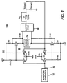
- FIGURE 1 is a diagram, in block and schematic form, of an amplifier circuit according to an inventive arrangement taught herein.
- FIGURE 2 is a block diagram of a prior art arrangement utilized in amplifier circuits.
- a power amplifier 100 may comprise a predriver stage 30 which has an arrangement as shown in FIGURE 1.
- a predriver stage 30 may generally comprise first and second differential amplifiers 31 and 32, which drive a complementary push-pull stage 33.
- First differential amplifier 31 may generally comprise transistors Q66 and Q77 and resistors R114 and R129, and may be coupled to first and second sources of voltage potential, for example +45 V and -45 V.
- first and second sources of voltage potential for example +45 V and -45 V.
- Transistors Q66 and Q77 may, for example, have an industry part number BC546B.
- Second differential amplifier 32 may generally comprise transistors Q69 and Q70 and resistors R3 and R130, and may also be coupled to the first and second sources of voltage potential.
- Transistors Q69 and Q70 may, for example, have an industry part number BC556B.
- Complementary push-pull stage 33 may generally comprise transistors Q5 and Q7, resistors R5, R7, R139 and R140, and a biasing circuit 34.
- Transistors Q5 and Q7 may, for example, have industry part numbers MPSA92 and MPSA42, respectively.
- the biasing circuit 34 is used for determining a class of operation for output stage 40 and for minimizing crossover distortion associated with the output stage 40.
- the biasing circuit 34 may be of a conventional design, and is not discussed herein.
- convergence correction voltage waveform 20 is coupled to the first and second differential amplifiers 21 and 22 at the base electrodes of transistors Q70 and Q77 and sense voltage V SENSE is coupled to the first and second differential amplifiers 21 and 22 at the base electrodes of transistors Q66 and Q69.
- convergence correction voltage waveform 20 has an amplitude of approximately zero volts
- sense voltage V SENSE is equal to approximately zero volts
- a current flowing through resistor R114 is divided equally between transistors Q66 and Q77.
- a current flowing through resistor R3 is conducted equally by transistors Q69 and Q70.
- a voltage divider formed by resistors R5 and R139 biases the emitter electrode of transistor Q5 such that a voltage between the base and emitter electrodes of transistor Q5 is slightly less than the voltage at which transistor Q5 would begin to turn on.
- a voltage divider formed by resistors R7 and R140 biases the emitter electrode of transistor Q7 such that a voltage between the base and emitter electrodes of transistor Q7 is slightly less than the voltage at which transistor Q7 would begin to turn on.
- An insignificantly small, temperature-dependent common-mode current equal to, for example, a small percentage of 1 mA may flow from transistor Q5 to transistor Q7.
- the current conducted by transistor Q70 decreases as transistor Q70 becomes less conductive. Since the current flowing through resistor R3 remains constant, the current conducted by transistor Q69 increases by an amount that is equal to the decrease in current through transistor Q70. As transistor Q70 becomes less conductive, it supplies less current to the base electrode of transistor Q7, thereby turning off transistor Q7.
- transistor Q77 increases as transistor Q77 tends to become more conductive. Since the current flowing through resistor R114 remains constant, the current conducted by transistor Q66 decreases by an amount that is equal to the increase in current through transistor Q77. As transistor Q77 becomes more conductive, it draws more current from the base electrode of transistor Q5, thereby turning on transistor Q5.
- transistor Q77 decreases as transistor Q77 tends to become less conductive. Since the current flowing through resistor R114 remains constant, the current conducted by transistor Q66 increases by an amount that is equal to the decrease in current through transistor Q77. As transistor Q77 becomes less conductive, it draws less current from the base electrode of transistor Q5, thereby turning off transistor Q5.
- the voltage dividers formed by resistors R5 and R139 and by resistors R7 and R140 bias the emitters of transistors Q5 and Q7, respectively, so as to prevent a common-mode current from flowing through those two transistors. This has several advantageous consequences.
- the voltage dividers formed by resistors R5 and R139 and by resistors R7 and R140 bias the emitter electrodes of transistors Q5 and Q7, respectively, such that transistors Q5 and Q7 remain on the threshold of turning on, and only an insignificantly small, temperature-dependent common-mode current flows from transistor Q5 to transistor Q7.
- This is advantageous because it reduces the power dissipated within the predriver stage 30 and thereby increases the overall efficiency of power amplifier 100.
- the voltage dividers provided by resistors R5 and R139 and by resistors R7 and R140 also enhance the tendency of push-pull stage 33 to operate in a class B mode.
- transistor Q5 conducts and transistor Q7 does not conduct.
- the voltages at the collector electrodes of transistors Q5 and Q7 are both equal to approximately +45 V, and a current equal to approximately 2.6 mA flows through resistors R7 and R140.
- the voltage at the emitter electrode of transistor Q7 thus only changes over a range equal to approximately 180 mV as its collector voltage swings through the range defined by the first and second sources of voltage potential.
- transistor Q7 conducts and transistor Q5 does not conduct.
- the voltages at the collector electrodes of transistors Q5 and Q7 are both equal to approximately -45 V and, thus, a current equal to approximately 2.6 mA flows through resistors R5 and R139.
- the voltage at the emitter electrode of transistor Q5 thus only changes over a range equal to approximately 180 mV as its collector voltage swings through the range defined by the first and second sources of voltage potential.
- transistors Q5 and Q7 are protected because the voltage divider formed by resistors R5 and R139 constrains the voltage at the emitter electrode of transistor Q5 to change by only approximately 180 mV, as described above. If, on the other hand, transistor Q5 fails and becomes a short circuit, transistor Q7 is protected because the voltage divider formed by resistors R7 and R140 constrains the voltage at the emitter electrode of transistor Q7 to change by only approximately 180 mV.
- the voltage divider arrangements provided by resistors R5 and R139 and by resistors R7 and R140 provide the additional advantage of protecting transistors Q5 and Q7 from thermally-induced damage.
- the base-emitter voltage of a bipolar junction transistor has a negative temperature coefficient.
- the base-emitter voltage of the transistor decreases and, consequently, the current conducted by the transistor increases.
- the transistor dissipates power in the form of heat, which increases the temperature of the transistor.
- This increase in temperature causes an increase in current, which, in turn, causes a further increase in temperature. This process, referred to in the art as thermal runaway, eventually destroys the transistor.
- transistor Q5 begins to saturate and it conducts a larger current.
- the voltage divider defined by resistors R5 and R139 biases the emitter electrode of transistor Q5 to a lower voltage. As a result, the voltage between the emitter and base electrodes of transistor Q5 decreases and, consequently, the current conducted by transistor Q5 is reduced.
- transistor Q7 As the temperature of transistor Q7, for example, begins to increase, transistor Q7 begins to saturate and it conducts a larger current. Before this mechanism can lead to thermal runaway, however, the voltage divider defined by resistors R7 and R140 biases the emitter electrode of transistor Q7 to a higher voltage. As a result, the voltage between the base and emitter electrodes of transistor Q7 decreases and, consequently, the current conducted by transistor Q7 is reduced.
Landscapes
- Engineering & Computer Science (AREA)
- Power Engineering (AREA)
- Amplifiers (AREA)
- Details Of Television Scanning (AREA)
- Transforming Electric Information Into Light Information (AREA)
Applications Claiming Priority (2)
| Application Number | Priority Date | Filing Date | Title |
|---|---|---|---|
| US574023 | 1995-12-18 | ||
| US08/574,023 US5814953A (en) | 1995-12-18 | 1995-12-18 | Power amplifier predriver stage |
Publications (3)
| Publication Number | Publication Date |
|---|---|
| EP0780971A2 true EP0780971A2 (de) | 1997-06-25 |
| EP0780971A3 EP0780971A3 (de) | 1999-03-31 |
| EP0780971B1 EP0780971B1 (de) | 2002-05-02 |
Family
ID=24294376
Family Applications (1)
| Application Number | Title | Priority Date | Filing Date |
|---|---|---|---|
| EP96402753A Expired - Lifetime EP0780971B1 (de) | 1995-12-18 | 1996-12-16 | Leistungsverstärkervortreiberstufe |
Country Status (7)
| Country | Link |
|---|---|
| US (1) | US5814953A (de) |
| EP (1) | EP0780971B1 (de) |
| JP (2) | JP3739149B2 (de) |
| KR (1) | KR100422225B1 (de) |
| CN (1) | CN1080026C (de) |
| ES (1) | ES2176418T3 (de) |
| MY (1) | MY119500A (de) |
Cited By (1)
| Publication number | Priority date | Publication date | Assignee | Title |
|---|---|---|---|---|
| US5913458A (en) * | 1994-11-16 | 1999-06-22 | Kvaerner Pulping Ab | Apparatus for adjusting the axial position of a rotary feeder |
Families Citing this family (4)
| Publication number | Priority date | Publication date | Assignee | Title |
|---|---|---|---|---|
| US6512340B1 (en) * | 2001-09-07 | 2003-01-28 | National Semiconductor Corporation | Temperature sensor with current mode output for thermal protection for a cathode ray tube (CRT) driver |
| JP2005520385A (ja) * | 2002-03-13 | 2005-07-07 | コーニンクレッカ フィリップス エレクトロニクス エヌ ヴィ | 種々のモードを有する前段増幅器 |
| JP4353759B2 (ja) * | 2003-09-22 | 2009-10-28 | Necエレクトロニクス株式会社 | 駆動回路 |
| CN101573864B (zh) * | 2006-10-30 | 2012-04-04 | 北方电讯网络有限公司 | 高效数字功率放大器 |
Family Cites Families (12)
| Publication number | Priority date | Publication date | Assignee | Title |
|---|---|---|---|---|
| US2863008A (en) * | 1954-08-27 | 1958-12-02 | Gen Electric | Stabilized amplifier |
| GB1059112A (en) * | 1963-08-20 | 1967-02-15 | British Broadcasting Corp | Improvements in and relating to buffer amplifiers |
| FR2398408A1 (fr) * | 1977-07-21 | 1979-02-16 | Cit Alcatel | Circuit de limitation de la tension de sortie d'un amplificateur |
| US4318052A (en) * | 1979-11-30 | 1982-03-02 | Hughes Aircraft Company | Wideband high voltage video amplifier |
| JPS5753113A (en) * | 1980-09-17 | 1982-03-30 | Pioneer Electronic Corp | Push-pull amplifier |
| US4483016A (en) * | 1982-09-23 | 1984-11-13 | Hochstein Peter A | Audio amplifier |
| US4644288A (en) * | 1985-01-09 | 1987-02-17 | Crown International, Inc. | Method of fault sensing for power amplifiers having coupled power stages with normally alternate current flow |
| US4719393A (en) * | 1986-09-02 | 1988-01-12 | Mccanney Neil R | Deflection amplifier |
| JP3188034B2 (ja) * | 1993-04-27 | 2001-07-16 | 三洋電機株式会社 | 増幅回路 |
| KR0138365B1 (ko) * | 1993-06-23 | 1998-05-15 | 김광호 | 출력회로 |
| EP0684698B1 (de) * | 1994-05-23 | 1999-11-17 | STMicroelectronics S.r.l. | Verstärkerausgangsstufe der Klasse "AB" |
| US5798668A (en) * | 1995-11-28 | 1998-08-25 | Thomson Consumer Electronics, Inc. | Low-power transconductance driver amplifier |
-
1995
- 1995-12-18 US US08/574,023 patent/US5814953A/en not_active Expired - Fee Related
-
1996
- 1996-12-05 MY MYPI96005099A patent/MY119500A/en unknown
- 1996-12-13 JP JP33417696A patent/JP3739149B2/ja not_active Expired - Fee Related
- 1996-12-16 ES ES96402753T patent/ES2176418T3/es not_active Expired - Lifetime
- 1996-12-16 EP EP96402753A patent/EP0780971B1/de not_active Expired - Lifetime
- 1996-12-17 KR KR1019960066581A patent/KR100422225B1/ko not_active Expired - Fee Related
- 1996-12-17 CN CN96117937A patent/CN1080026C/zh not_active Expired - Fee Related
-
2005
- 2005-09-21 JP JP2005273587A patent/JP2006014379A/ja active Pending
Non-Patent Citations (1)
| Title |
|---|
| None |
Cited By (1)
| Publication number | Priority date | Publication date | Assignee | Title |
|---|---|---|---|---|
| US5913458A (en) * | 1994-11-16 | 1999-06-22 | Kvaerner Pulping Ab | Apparatus for adjusting the axial position of a rotary feeder |
Also Published As
| Publication number | Publication date |
|---|---|
| JP2006014379A (ja) | 2006-01-12 |
| KR100422225B1 (ko) | 2004-07-23 |
| JPH09312817A (ja) | 1997-12-02 |
| CN1080026C (zh) | 2002-02-27 |
| ES2176418T3 (es) | 2002-12-01 |
| KR970055262A (ko) | 1997-07-31 |
| EP0780971A3 (de) | 1999-03-31 |
| JP3739149B2 (ja) | 2006-01-25 |
| MY119500A (en) | 2005-06-30 |
| US5814953A (en) | 1998-09-29 |
| CN1157505A (zh) | 1997-08-20 |
| EP0780971B1 (de) | 2002-05-02 |
Similar Documents
| Publication | Publication Date | Title |
|---|---|---|
| US5798668A (en) | Low-power transconductance driver amplifier | |
| US5814953A (en) | Power amplifier predriver stage | |
| JP3196117B2 (ja) | 双対電源出力増幅器 | |
| JPH0918743A (ja) | 陰極線管駆動装置 | |
| JP3628050B2 (ja) | ビーム走査速度変調を有する画像表示装置 | |
| MXPA96006642A (en) | Ener amplifier precontroller stage | |
| EP0562683B1 (de) | Anzeigevorrichtung mit Bildröhre einschlisslich einer Kaltkathode | |
| US6002453A (en) | Deflection with low offset | |
| GB2145595A (en) | Wideband amplifier | |
| JP3804991B2 (ja) | ビーム電流制限を自動調節するビデオ出力段 | |
| US3748525A (en) | Vertical convergence circuits utilizing positive feedback for stabilization | |
| US6369528B1 (en) | Vertical deflection circuit | |
| KR0138365B1 (ko) | 출력회로 | |
| JP2599790B2 (ja) | 水平偏向回路 | |
| US6294884B1 (en) | Vertical deflection circuit and color picture tube apparatus | |
| US4719393A (en) | Deflection amplifier | |
| WO1999031876A1 (en) | Display driver apparatus | |
| EP0870399B1 (de) | Ablenkung mit kompensation der dämpfungsimpedanz | |
| KR19990052757A (ko) | 모니터의 지오메트리 디스토션 보정회로 | |
| JPS6017192B2 (ja) | 垂直偏向回路 | |
| US7110234B2 (en) | Power supply protection arrangement | |
| KR20000014588U (ko) | 모니터의 틸트 보정회로 | |
| JP3330806B2 (ja) | 音揺れ防止回路 | |
| JP2005528825A (ja) | 陰極線管用の補助コイルドライバ回路 | |
| JPH0242886A (ja) | 両極性のこぎり波電力増幅回路 |
Legal Events
| Date | Code | Title | Description |
|---|---|---|---|
| PUAI | Public reference made under article 153(3) epc to a published international application that has entered the european phase |
Free format text: ORIGINAL CODE: 0009012 |
|
| AK | Designated contracting states |
Kind code of ref document: A2 Designated state(s): ES FR GB IT |
|
| PUAL | Search report despatched |
Free format text: ORIGINAL CODE: 0009013 |
|
| AK | Designated contracting states |
Kind code of ref document: A3 Designated state(s): ES FR GB IT |
|
| 17P | Request for examination filed |
Effective date: 19990913 |
|
| 17Q | First examination report despatched |
Effective date: 20001107 |
|
| GRAG | Despatch of communication of intention to grant |
Free format text: ORIGINAL CODE: EPIDOS AGRA |
|
| GRAG | Despatch of communication of intention to grant |
Free format text: ORIGINAL CODE: EPIDOS AGRA |
|
| GRAH | Despatch of communication of intention to grant a patent |
Free format text: ORIGINAL CODE: EPIDOS IGRA |
|
| REG | Reference to a national code |
Ref country code: GB Ref legal event code: IF02 |
|
| GRAH | Despatch of communication of intention to grant a patent |
Free format text: ORIGINAL CODE: EPIDOS IGRA |
|
| GRAA | (expected) grant |
Free format text: ORIGINAL CODE: 0009210 |
|
| AK | Designated contracting states |
Kind code of ref document: B1 Designated state(s): ES FR GB IT |
|
| REG | Reference to a national code |
Ref country code: GB Ref legal event code: FG4D |
|
| ET | Fr: translation filed | ||
| ET | Fr: translation filed | ||
| REG | Reference to a national code |
Ref country code: ES Ref legal event code: FG2A Ref document number: 2176418 Country of ref document: ES Kind code of ref document: T3 |
|
| REG | Reference to a national code |
Ref country code: GB Ref legal event code: 746 Effective date: 20030103 |
|
| PLBE | No opposition filed within time limit |
Free format text: ORIGINAL CODE: 0009261 |
|
| STAA | Information on the status of an ep patent application or granted ep patent |
Free format text: STATUS: NO OPPOSITION FILED WITHIN TIME LIMIT |
|
| 26N | No opposition filed |
Effective date: 20030204 |
|
| PGFP | Annual fee paid to national office [announced via postgrant information from national office to epo] |
Ref country code: IT Payment date: 20081220 Year of fee payment: 13 |
|
| PGFP | Annual fee paid to national office [announced via postgrant information from national office to epo] |
Ref country code: ES Payment date: 20090120 Year of fee payment: 13 |
|
| PGFP | Annual fee paid to national office [announced via postgrant information from national office to epo] |
Ref country code: GB Payment date: 20081201 Year of fee payment: 13 |
|
| PGFP | Annual fee paid to national office [announced via postgrant information from national office to epo] |
Ref country code: FR Payment date: 20081219 Year of fee payment: 13 |
|
| GBPC | Gb: european patent ceased through non-payment of renewal fee |
Effective date: 20091216 |
|
| REG | Reference to a national code |
Ref country code: FR Ref legal event code: ST Effective date: 20100831 |
|
| PG25 | Lapsed in a contracting state [announced via postgrant information from national office to epo] |
Ref country code: FR Free format text: LAPSE BECAUSE OF NON-PAYMENT OF DUE FEES Effective date: 20091231 |
|
| PG25 | Lapsed in a contracting state [announced via postgrant information from national office to epo] |
Ref country code: GB Free format text: LAPSE BECAUSE OF NON-PAYMENT OF DUE FEES Effective date: 20091216 |
|
| PG25 | Lapsed in a contracting state [announced via postgrant information from national office to epo] |
Ref country code: IT Free format text: LAPSE BECAUSE OF NON-PAYMENT OF DUE FEES Effective date: 20091216 |
|
| REG | Reference to a national code |
Ref country code: ES Ref legal event code: FD2A Effective date: 20111116 |
|
| PG25 | Lapsed in a contracting state [announced via postgrant information from national office to epo] |
Ref country code: ES Free format text: LAPSE BECAUSE OF NON-PAYMENT OF DUE FEES Effective date: 20091217 |