EP0780751A2 - Leistungsfaktor-Steuerschaltung - Google Patents
Leistungsfaktor-Steuerschaltung Download PDFInfo
- Publication number
- EP0780751A2 EP0780751A2 EP96114376A EP96114376A EP0780751A2 EP 0780751 A2 EP0780751 A2 EP 0780751A2 EP 96114376 A EP96114376 A EP 96114376A EP 96114376 A EP96114376 A EP 96114376A EP 0780751 A2 EP0780751 A2 EP 0780751A2
- Authority
- EP
- European Patent Office
- Prior art keywords
- voltage
- input
- power factor
- controller circuit
- factor controller
- Prior art date
- Legal status (The legal status is an assumption and is not a legal conclusion. Google has not performed a legal analysis and makes no representation as to the accuracy of the status listed.)
- Withdrawn
Links
Images
Classifications
-
- H—ELECTRICITY
- H02—GENERATION; CONVERSION OR DISTRIBUTION OF ELECTRIC POWER
- H02M—APPARATUS FOR CONVERSION BETWEEN AC AND AC, BETWEEN AC AND DC, OR BETWEEN DC AND DC, AND FOR USE WITH MAINS OR SIMILAR POWER SUPPLY SYSTEMS; CONVERSION OF DC OR AC INPUT POWER INTO SURGE OUTPUT POWER; CONTROL OR REGULATION THEREOF
- H02M1/00—Details of apparatus for conversion
- H02M1/42—Circuits or arrangements for compensating for or adjusting power factor in converters or inverters
- H02M1/4208—Arrangements for improving power factor of AC input
- H02M1/4225—Arrangements for improving power factor of AC input using a non-isolated boost converter
-
- H—ELECTRICITY
- H02—GENERATION; CONVERSION OR DISTRIBUTION OF ELECTRIC POWER
- H02M—APPARATUS FOR CONVERSION BETWEEN AC AND AC, BETWEEN AC AND DC, OR BETWEEN DC AND DC, AND FOR USE WITH MAINS OR SIMILAR POWER SUPPLY SYSTEMS; CONVERSION OF DC OR AC INPUT POWER INTO SURGE OUTPUT POWER; CONTROL OR REGULATION THEREOF
- H02M1/00—Details of apparatus for conversion
- H02M1/0003—Details of control, feedback or regulation circuits
-
- H—ELECTRICITY
- H02—GENERATION; CONVERSION OR DISTRIBUTION OF ELECTRIC POWER
- H02M—APPARATUS FOR CONVERSION BETWEEN AC AND AC, BETWEEN AC AND DC, OR BETWEEN DC AND DC, AND FOR USE WITH MAINS OR SIMILAR POWER SUPPLY SYSTEMS; CONVERSION OF DC OR AC INPUT POWER INTO SURGE OUTPUT POWER; CONTROL OR REGULATION THEREOF
- H02M3/00—Conversion of DC power input into DC power output
- H02M3/02—Conversion of DC power input into DC power output without intermediate conversion into AC
- H02M3/04—Conversion of DC power input into DC power output without intermediate conversion into AC by static converters
- H02M3/10—Conversion of DC power input into DC power output without intermediate conversion into AC by static converters using discharge tubes with control electrode or semiconductor devices with control electrode
- H02M3/145—Conversion of DC power input into DC power output without intermediate conversion into AC by static converters using discharge tubes with control electrode or semiconductor devices with control electrode using devices of a triode or transistor type requiring continuous application of a control signal
- H02M3/155—Conversion of DC power input into DC power output without intermediate conversion into AC by static converters using discharge tubes with control electrode or semiconductor devices with control electrode using devices of a triode or transistor type requiring continuous application of a control signal using semiconductor devices only
- H02M3/156—Conversion of DC power input into DC power output without intermediate conversion into AC by static converters using discharge tubes with control electrode or semiconductor devices with control electrode using devices of a triode or transistor type requiring continuous application of a control signal using semiconductor devices only with automatic control of output voltage or current, e.g. switching regulators
-
- Y—GENERAL TAGGING OF NEW TECHNOLOGICAL DEVELOPMENTS; GENERAL TAGGING OF CROSS-SECTIONAL TECHNOLOGIES SPANNING OVER SEVERAL SECTIONS OF THE IPC; TECHNICAL SUBJECTS COVERED BY FORMER USPC CROSS-REFERENCE ART COLLECTIONS [XRACs] AND DIGESTS
- Y02—TECHNOLOGIES OR APPLICATIONS FOR MITIGATION OR ADAPTATION AGAINST CLIMATE CHANGE
- Y02B—CLIMATE CHANGE MITIGATION TECHNOLOGIES RELATED TO BUILDINGS, e.g. HOUSING, HOUSE APPLIANCES OR RELATED END-USER APPLICATIONS
- Y02B70/00—Technologies for an efficient end-user side electric power management and consumption
- Y02B70/10—Technologies improving the efficiency by using switched-mode power supplies [SMPS], i.e. efficient power electronics conversion e.g. power factor correction or reduction of losses in power supplies or efficient standby modes
-
- Y—GENERAL TAGGING OF NEW TECHNOLOGICAL DEVELOPMENTS; GENERAL TAGGING OF CROSS-SECTIONAL TECHNOLOGIES SPANNING OVER SEVERAL SECTIONS OF THE IPC; TECHNICAL SUBJECTS COVERED BY FORMER USPC CROSS-REFERENCE ART COLLECTIONS [XRACs] AND DIGESTS
- Y02—TECHNOLOGIES OR APPLICATIONS FOR MITIGATION OR ADAPTATION AGAINST CLIMATE CHANGE
- Y02P—CLIMATE CHANGE MITIGATION TECHNOLOGIES IN THE PRODUCTION OR PROCESSING OF GOODS
- Y02P80/00—Climate change mitigation technologies for sector-wide applications
- Y02P80/10—Efficient use of energy, e.g. using compressed air or pressurized fluid as energy carrier
Definitions
- This invention relates to power factor controller circuits.
- PFC circuits are typically used within power supply applications, and may comprise a voltage rectifier circuit and a bulk capacitor. PFC circuits are incorporated to reduce the problems associated with current drain. However, with such PFC circuits, current is only drawn while the bulk capacitor is being charged, resulting in an inefficient current profile, including high current peaks which produce much adverse noise.
- a known solution to mitigate the problem of the inefficient current profile is to employ a pre-regulator stage in which the bulk capacitor is replaced by a large capacitor/inductor circuit, and a power switch and diode arrangement.
- Such an arrangement is known as a boost configuration, since the output voltage level always exceeds the instantaneous input voltage level.
- this approach is very expensive, due to the size and number of components used.
- This invention seeks to provide a power factor controller circuit which mitigates the above mentioned disadvantages.
- a power factor controller circuit comprising: a rectified voltage input; a switched inductor arrangement coupled to the rectified voltage input, for providing an output voltage; control means for switching the switched inductor arrangement according to a control input; and, feedback means, arranged for comparing a portion of the output voltage with a weighted parameter of the input voltage, and for providing an error voltage to the control input for regulating the switched inductor, wherein the feedback means includes sensing means for sensing the parameter of the input voltage and weighting means for weighting the parameter of the input voltage by a predetermined fixed voltage.
- the parameter of the input voltage is an average value thereof.
- the parameter of the input voltage is a peak value thereof.
- the weighting means includes an adder circuit, arranged to add the predetermined fixed voltage to the parameter of the input voltage, thereby providing the weighted parameter of the input voltage.
- the weighting means includes a subtraction circuit, arranged to subtract the predetermined fixed voltage from the parameter of the input voltage, thereby providing the weighted parameter of the input voltage.
- the switched inductor arrangement comprises an inductor arranged in dependence upon the predetermined fixed voltage.
- the feedback means preferably includes an error amplifier having an inverting input coupled to the output voltage, a non-inverting input coupled to the weighting means and an output for providing the error voltage.
- the predetermined fixed voltage is positive.
- the predetermined fixed voltage is negative.
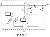
- a power factor controller circuit 10 including a rectified voltage input terminal 20, a switched inductor arrangement 30 coupled to the rectified voltage input terminal 20, an output terminal 40, coupled to the switched inductor arrangement 30 and a feedback path.
- a capacitor 36 is coupled between the output terminal 40 and ground.
- the switched inductor arrangement comprises an inductor 32, a switch 33 and a diode 37.
- a first terminal of the inductor 32 is coupled to the rectified voltage input terminal 20.
- the diode 37 is coupled between a second terminal of the inductor 32 and the output terminal 40.
- the switch 33 has a first switched input coupled to a ground reference, a second switched input coupled to a node between the second terminal of the inductor 32 and the diode 37, and a control input to be further described below. In this way the switch 33 is arranged for selectively coupling the node to ground.
- the feedback path comprises a scaling circuit 80, an error amplifier 50, a control circuit 35, a sensing circuit 70 and an adder circuit 60.
- the sensing circuit 70 is coupled to sense the input voltage from the rectified voltage input terminal 20.
- the adder circuit 60 is arranged to receive a sensed voltage signal from the sensing circuit 70 and a reference voltage 65, in order to provide a summed output thereof.
- the scaling circuit 80 is coupled to the output terminal 40, for providing a scaled value of the output voltage.
- the error amplifier circuit 50 has an inverting input coupled to receive the scaled output voltage from the scaling circuit 80, a non-inverting input coupled to receive the summed output and an output coupled to the control input of the switch 33 via the control circuit 35.
- a rectified voltage is received at the rectified voltage input 20.
- the sensing circuit 70 is arranged to detect the average value of the rectified voltage and to provide a scaled voltage representing this average value to the adder circuit 60.
- a predetermined voltage ⁇ V 65 is added to the average value voltage within the adder circuit 60, producing a summed voltage which is provided to the non-inverting terminal of the error amplifier 50. The summed voltage is therefore equal to sum of the average value voltage and ⁇ V 65.
- the rectified voltage also induces a current in inductor 32 and when the switch 33 is open, current flows through the inductor 32 and the diode 37 to the output terminal 40.
- the switch 33 When the switch 33 is dosed, current flows through the inductor 32 and switch 33 to ground. The diode 37 is then reverse biased, and no current flows therein.
- the voltage at the output terminal 40 is sensed by the scaling circuit 80, which provides the scaled value to the inverting terminal of the error amplifier 50.
- the error amplifier 50 produces an error signal derived from the inverting and non-inverting inputs.
- the control circuit 35 is arranged to provide control signals to the switch 33 in response to the value of the error signal. In this way regulation of the circuit 10 is achieved.
- the value of the inductor 32 can be readily chosen in conjunction with the value of ⁇ V 65, and the relative scaling factors used by the sensing circuit 70 and the scaling circuit 80, as shown by the following equations:-
- L Vin(t).T Ipk . 1 - Vin(t) Kin Ko ⁇ Vin av + ⁇ V Ko
- Equation 7 demonstrates that for a given period T, and a given current Ipk, the value L of the inductor 32 may be reduced when Kin Ko ⁇ Vin av + ⁇ V Ko tends towards Vin(t), taking into account that Vo must always be higher than Vin(t).
- Appropriate values are chosen for the sensing circuit 70 (Kin), the scaling circuit 80 (Ko) and ⁇ V, to produce an optimal output voltage very near Vin(t), while always remaining greater than the instantaneous value of the input voltage at the input terminal 20. In this way, the size of inductor 32 can be kept to a minimum. In other working modes, such as a continuous working mode, similar conditions apply, and produce a similar reduction in the size of the inductor 32.
- the fixed voltage ⁇ V 65 could be either positive or negative.
- the adder circuit 60 may be replaced by a subtraction circuit arranged to subtract ⁇ V 65.
- the error amplifier 50 could be replaced by an alternative arrangement such as a microprocessor.
- the sensing circuit 70 could be arranged to sense a parameter of the input voltage other than the average value, such as a peak value.
Landscapes
- Engineering & Computer Science (AREA)
- Power Engineering (AREA)
- Rectifiers (AREA)
- Dc-Dc Converters (AREA)
Applications Claiming Priority (2)
| Application Number | Priority Date | Filing Date | Title |
|---|---|---|---|
| GB9526314 | 1995-12-22 | ||
| GB9526314A GB2308685A (en) | 1995-12-22 | 1995-12-22 | Power factor controller circuit |
Publications (2)
| Publication Number | Publication Date |
|---|---|
| EP0780751A2 true EP0780751A2 (de) | 1997-06-25 |
| EP0780751A3 EP0780751A3 (de) | 1998-05-20 |
Family
ID=10785919
Family Applications (1)
| Application Number | Title | Priority Date | Filing Date |
|---|---|---|---|
| EP96114376A Withdrawn EP0780751A3 (de) | 1995-12-22 | 1996-09-09 | Leistungsfaktor-Steuerschaltung |
Country Status (5)
| Country | Link |
|---|---|
| EP (1) | EP0780751A3 (de) |
| JP (1) | JPH09205767A (de) |
| KR (1) | KR970055155A (de) |
| GB (1) | GB2308685A (de) |
| HU (1) | HUP9603523A2 (de) |
Families Citing this family (1)
| Publication number | Priority date | Publication date | Assignee | Title |
|---|---|---|---|---|
| KR100698636B1 (ko) * | 2005-04-15 | 2007-03-22 | 한국생산기술연구원 | 비대칭 다-곡률 마이크로렌즈 제조 방법 및 이의 방법에 의해 제조된 도광판 |
Family Cites Families (3)
| Publication number | Priority date | Publication date | Assignee | Title |
|---|---|---|---|---|
| GB8905177D0 (en) * | 1989-03-07 | 1989-04-19 | Emi Plc Thorn | Switched-mode regulator circuit |
| GB9104070D0 (en) * | 1991-02-27 | 1991-04-17 | Astec Int Ltd | Power supplies |
| DE4340604A1 (de) * | 1993-08-25 | 1995-03-02 | Tridonic Bauelemente Ges Mbh | Elektronisches Vorschaltgerät zum Versorgen einer Last, beispielsweise einer Lampe |
-
1995
- 1995-12-22 GB GB9526314A patent/GB2308685A/en not_active Withdrawn
-
1996
- 1996-09-09 EP EP96114376A patent/EP0780751A3/de not_active Withdrawn
- 1996-12-13 JP JP8352754A patent/JPH09205767A/ja active Pending
- 1996-12-19 HU HU9603523A patent/HUP9603523A2/hu unknown
- 1996-12-19 KR KR1019960067662A patent/KR970055155A/ko not_active Withdrawn
Also Published As
| Publication number | Publication date |
|---|---|
| JPH09205767A (ja) | 1997-08-05 |
| KR970055155A (ko) | 1997-07-31 |
| GB9526314D0 (en) | 1996-02-21 |
| HUP9603523A2 (en) | 1997-08-28 |
| HU9603523D0 (en) | 1997-02-28 |
| GB2308685A (en) | 1997-07-02 |
| EP0780751A3 (de) | 1998-05-20 |
Similar Documents
| Publication | Publication Date | Title |
|---|---|---|
| US4525774A (en) | Regulated AC-DC converter having saturation inductance in resonant circuit | |
| KR101030798B1 (ko) | 역률 보상 회로 | |
| CN100334800C (zh) | 电源转换器所需的具有关闭周期调节功能的pwm控制器 | |
| US6344986B1 (en) | Topology and control method for power factor correction | |
| KR100718828B1 (ko) | Llc 컨버터 및 llc 컨버터를 제어하기 위한 방법 | |
| US5572112A (en) | Power supply unit | |
| CA2142206A1 (en) | Current controller using hall device for controlling current in a switchmode circuit | |
| EP0593257A2 (de) | Verstärkerwandler | |
| US6177782B1 (en) | Circuit and method of controlling a regulator with an output feedback signal and devoid of an input feedforward signal | |
| JPH03124215A (ja) | 過電流保護装置 | |
| US5291119A (en) | Low distortion alternating current output active power factor correction circuit using two bi-directional switching regulations | |
| US20030071636A1 (en) | Method and apparatus for near losslessly measuring inductor current | |
| EP0370388B1 (de) | Leistungskonverter | |
| US5359277A (en) | Low distortion alternating current output active power factor correction circuit using bi-directional bridge rectifier and bi-directional switching regulator | |
| JP2005287249A (ja) | スイッチング電源装置 | |
| US6037754A (en) | SMPS with input voltage sensing via boost inductor current sensing | |
| EP0780751A2 (de) | Leistungsfaktor-Steuerschaltung | |
| EP0534422A2 (de) | Stromversorgungsvorrichtung | |
| AU2003267772A1 (en) | Power converter | |
| JPH09271165A (ja) | スイッチング電源装置 | |
| EP0665632A2 (de) | Schalt-Stromversorgungsgerät | |
| US6697269B2 (en) | Single-stage converter compensating power factor | |
| US12155312B2 (en) | Power converter controller, power converter and method for operating control of a power stage based on an intermediate voltage with respect to a threshold value determined from a turns ratio of a transformer | |
| JPH09121534A (ja) | Dc/dcコンバータ | |
| KR20200078110A (ko) | 양극성 펄스 전원 공급 장치 |
Legal Events
| Date | Code | Title | Description |
|---|---|---|---|
| PUAI | Public reference made under article 153(3) epc to a published international application that has entered the european phase |
Free format text: ORIGINAL CODE: 0009012 |
|
| AK | Designated contracting states |
Kind code of ref document: A2 Designated state(s): DE FR IT NL |
|
| PUAL | Search report despatched |
Free format text: ORIGINAL CODE: 0009013 |
|
| AK | Designated contracting states |
Kind code of ref document: A3 Designated state(s): DE FR IT NL |
|
| STAA | Information on the status of an ep patent application or granted ep patent |
Free format text: STATUS: THE APPLICATION IS DEEMED TO BE WITHDRAWN |
|
| 18D | Application deemed to be withdrawn |
Effective date: 19981121 |